Drivers, Receivers, Transceivers
بەرهەمەکان (5)

ISO1432DW - 12Mbps Isolated Full-Duplex RS-485/RS-422 Transceiver | TI
The Texas Instruments ISO1432DW is an EMC-protected, 12-Mbps, full-duplex, 5-kVrms isolated RS-485 and RS-422 transceiver housed in a 16-pin SOIC (DW) package. The device integrates a galvanic isolation barrier with reinforced insulation rated at 5 kVrms, a 1/1 (one driver, one receiver) full-duplex channel, and TI's proprietary EMC hardening for industrial bus robustness. Operating from a 3 V to 5.5 V supply, it supports data rates up to 12 Mbps and replaces discrete opto-isolator plus transceiver solutions with a single IC. An isolated RS-485 transceiver is a galvanically-isolated differential line driver/receiver designed for TIA/EIA-485-A and TIA/EIA-422-A applications. Within a system hierarchy, it sits at the interface between a low-voltage controller (MCU, FPGA, DSP) and a long-distance, noise-prone industrial bus. The isolation barrier blocks high-voltage transients, ground-potential differences, and common-mode noise that would otherwise couple into sensitive digital or analog circuitry upstream. By eliminating external optocouplers and isolated DC/DC converters (when paired with an integrated power isolator companion), the ISO1432 simplifies BOM, reduces board area, and improves reliability versus discrete implementations. Key features include 5-kVrms reinforced isolation per UL 1577, 12 Mbps maximum signaling rate, 1/1 full-duplex topology with separate driver output (Y/Z) and receiver input (A/B) pins, integrated bus protection including IEC 61000-4-2 ESD (typically 8 kV contact / 15 kV air) and IEC 61000-4-4 electrical fast transient immunity, and a wide 3 V to 5.5 V supply range. The device operates across -40 °C to +125 °C, suiting outdoor, cabinet-mounted, and motor-drive environments. The 16-pin DW SOIC footprint provides a creepage/clearance distance consistent with reinforced insulation requirements, simplifying PCB layout for high-voltage spacing. Internally, the ISO1432 uses TI's silicon-oxide (SiO2) capacitive isolation barrier combined with an RS-485 transceiver die on each side. The high-speed differential driver delivers 1.5 V minimum output swing into a 54 Ω load per TIA/EIA-485, while the receiver offers 50 mV typical hysteresis and a 1/8-unit-load input impedance (allowing up to 256 nodes on the bus when used with other 1/8-load parts). The EMC hardening includes spread-spectrum OOK signaling across the barrier and integrated surge protection on the bus pins, eliminating the need for external TVS diodes in many applications. Typical applications include industrial programmable logic controllers (PLCs), factory automation and field-bus networks, motor-control inverter gate-driver communication, solar inverter H-bridge control interfaces, building-automation RS-485 trunks, and any microcontroller-to-bus interface requiring reinforced isolation. The wide temperature range also suits outdoor instrumentation and renewable-energy installations. When designing with the ISO1432, allocate at least 8 mm of creepage on the PCB beneath and between the SOIC package sides to preserve the 5 kVrms rating, and pair the part with a wide-Vin isolated DC/DC (such as the ISOW1044 or ISOW1412 companion families) when the bus side must remain powered during MCU brownouts. Decouple both VCC1 and VCC2 with 1 µF X7R ceramic capacitors placed within 2 mm of the supply pins to keep digital switching currents off the isolation barrier. This page synthesizes distributor pricing, drop-in alternatives, and practical design notes not found in the standalone manufacturer datasheet.
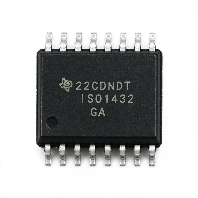
ISO1432DWR - 12Mbps Isolated Full-Duplex RS-485/RS-422 Transceiver | TI (Tape & Reel)
The Texas Instruments ISO1432DWR is an EMC-protected, 12-Mbps, full-duplex, 5-kVrms isolated RS-485 and RS-422 transceiver housed in a 16-pin SOIC (DW) package. The device integrates a galvanic isolation barrier with reinforced insulation rated at 5 kVrms, a 1/1 (one driver, one receiver) full-duplex channel, and TI's proprietary EMC hardening for industrial bus robustness. Operating from a 3 V to 5.5 V supply, it supports data rates up to 12 Mbps and replaces discrete opto-isolator plus transceiver solutions with a single IC. An isolated RS-485 transceiver is a galvanically-isolated differential line driver/receiver designed for TIA/EIA-485-A and TIA/EIA-422-A applications. Within a system hierarchy, it sits at the interface between a low-voltage controller (MCU, FPGA, DSP) and a long-distance, noise-prone industrial bus. The isolation barrier blocks high-voltage transients, ground-potential differences, and common-mode noise that would otherwise couple into sensitive digital or analog circuitry upstream. By eliminating external optocouplers and isolated DC/DC converters (when paired with an integrated power isolator companion), the ISO1432 simplifies BOM, reduces board area, and improves reliability versus discrete implementations. Key features include 5-kVrms reinforced isolation per UL 1577, 12 Mbps maximum signaling rate, 1/1 full-duplex topology with separate driver output (Y/Z) and receiver input (A/B) pins, integrated bus protection including IEC 61000-4-2 ESD (typically 8 kV contact / 15 kV air) and IEC 61000-4-4 electrical fast transient immunity, and a wide 3 V to 5.5 V supply range. The device operates across -40 °C to +125 °C, suiting outdoor, cabinet-mounted, and motor-drive environments. The 16-pin DW SOIC footprint provides a creepage/clearance distance consistent with reinforced insulation requirements, simplifying PCB layout for high-voltage spacing. Internally, the ISO1432 uses TI's silicon-oxide (SiO2) capacitive isolation barrier combined with an RS-485 transceiver die on each side. The high-speed differential driver delivers 1.5 V minimum output swing into a 54 Ω load per TIA/EIA-485, while the receiver offers 50 mV typical hysteresis and a 1/8-unit-load input impedance (allowing up to 256 nodes on the bus when used with other 1/8-load parts). The EMC hardening includes spread-spectrum OOK signaling across the barrier and integrated surge protection on the bus pins, eliminating the need for external TVS diodes in many applications. Typical applications include industrial programmable logic controllers (PLCs), factory automation and field-bus networks, motor-control inverter gate-driver communication, solar inverter H-bridge control interfaces, building-automation RS-485 trunks, and any microcontroller-to-bus interface requiring reinforced isolation. The wide temperature range also suits outdoor instrumentation and renewable-energy installations. When designing with the ISO1432, allocate at least 8 mm of creepage on the PCB beneath and between the SOIC package sides to preserve the 5 kVrms rating, and pair the part with a wide-Vin isolated DC/DC (such as the ISOW1044 or ISOW1412 companion families) when the bus side must remain powered during MCU brownouts. Decouple both VCC1 and VCC2 with 1 µF X7R ceramic capacitors placed within 2 mm of the supply pins to keep digital switching currents off the isolation barrier. This page synthesizes distributor pricing, drop-in alternatives, and practical design notes not found in the standalone manufacturer datasheet.

MAX232ECN - Dual RS-232 Transceiver, ESD Protected | TI
The Texas Instruments MAX232ECN is a dual-channel RS-232 line driver/receiver transceiver operating from a single 4.5V to 5.5V supply, delivering 250kbps data rates in a 16-pin PDIP (DIP-16) package with enhanced IEC61000-4-2 ESD protection on the RS-232 lines. An RS-232 transceiver is an interface IC that converts TTL/CMOS logic levels (0V to 5V) to the TIA/EIA-232-F voltage levels (approximately +/-5V to +/-15V) required for serial communication between equipment such as terminals, modems, and embedded microcontroller ports. Within the interface IC hierarchy, the MAX232 family is the industry-standard solution for short-haul asynchronous serial links, sitting between a UART and the physical RS-232 cable connector. Key features include a capacitive charge-pump voltage generator that develops the +/-9V RS-232 output swings from a single 5V rail, eliminating the need for bipolar supplies. Each receiver converts RS-232 inputs down to 5V TTL/CMOS levels with a typical 1.3V threshold, 0.5V typical hysteresis for noise immunity, and the ability to withstand +/-30V input swings. The E-grade device adds enhanced ESD robustness per IEC61000-4-2 on the transceiver lines. Architecturally, the part contains two drivers and two receivers (2/2 configuration) plus two charge pumps requiring only four small external capacitors. According to the TI MAX232 datasheet, low operating supply current of typically 8mA makes it practical for battery-backed and industrial serial ports, while the 250kbps maximum data rate covers the vast majority of legacy serial applications. Typical applications include legacy RS-232 ports on industrial equipment, point-of-sale terminals, motor drives and PLC serial debugging consoles, and telecom/modem interfaces. It is the go-to part for adding a robust serial port to a 5V microcontroller such as the PIC24 or XMC families. Design-wise, use four 0.1uF charge-pump capacitors (or follow the capacitor value table in the datasheet for higher data rates), keep the capacitors close to pins 1-6, and place a 1uF bulk capacitor on VCC. Never exceed the +/-30V receiver input rating. This page adds value beyond the datasheet by synthesizing drop-in alternatives, per-application selection guidance, and practical design notes in one place.

TCAN1051VDRBTQ1 - CAN FD Transceiver, 8Mbps, VSON-8 | TI
The Texas Instruments TCAN1051VDRBTQ1 is an automotive-grade fault-protected CAN transceiver with CAN Flexible Data-Rate (CAN FD) support, housed in an 8-pin VSON (DRB) 3x3 mm package. It operates from a 4.5 V to 5.5 V VCC supply, tolerates up to +/-58 V bus fault conditions, and supports CAN FD signaling up to 8 Mbps, with AEC-Q100 qualification for -40C to +125C (Grade 1, -55C capable per datasheet). A CAN transceiver is a physical-layer interface IC that converts the TTL-level logic signals of a CAN controller (TXD, RXD) into the differential CAN bus signals (CANH, CANL) defined by ISO 11898-2. Within the system hierarchy, it sits between the host MCU and the twisted-pair bus, providing the dominant/recessive drive levels, bus termination interface, receiver thresholds, and fault protection that a controller cannot supply directly. Key features include the VIO pin, which adapts the TXD/RXD logic levels for 1.8 V, 3.3 V, or 5 V microcontrollers without external level shifting; extended bus fault protection of +/-58 V against battery reversals and load-dump events on 12 V and 24 V vehicles; and silent-mode/standby operation for low system power. The device meets or exceeds the ISO 11898-2 physical layer requirements and supports 2 Mbps network operation as stated in distributor listings. Technically, the TCAN1051 family uses a bipolar-CMOS-DMOS process with robust drivers that survive short circuits of CANH or CANL to ground, battery, or each other, and an integrated protection scheme covering overvoltage and loss-of-ground conditions. Receiver timing symmetry is designed for CAN FD, allowing reliable sampling on arbitration-phase and data-phase bits. Typical applications include automotive body control modules, electric power steering, battery management systems (with companion devices like the BQ76952PFBR), and industrial gateways where EMC robustness and fault protection are critical. Design consideration: place a 100 pF to 220 pF common-mode capacitor and split termination near the transceiver, and verify that the VIO rail is present before the CAN controller drives TXD. This page synthesizes distributor pricing, same-family drop-in alternatives, pinout, and practical design notes not found in the manufacturer datasheet alone.

TJA1083GTT/0Z - FlexRay Clamp 15 Transceiver | NXP
The NXP Semiconductors TJA1083GTT/0Z is a FlexRay node transceiver (Clamp 15 type) compliant with the FlexRay Electrical Physical Layer specification ISO 17458-4:2013 (V3.0.1), housed in a 14-pin TSSOP surface-mount package, supporting communication systems operating at data rates between 2.5 Mbit/s and 10 Mbit/s. A FlexRay node transceiver is a specialized interface device that connects a FlexRay protocol controller to the vehicle's FlexRay differential bus. As a sub-category of line drivers/receivers in the automotive in-vehicle networking hierarchy (transceiver -> bus interface IC -> automotive networking IC -> semiconductor), it translates the controller's logic-level transmit data into differential bus signals and recovers received data for the controller. The FlexRay standard is used in time-triggered, fault-tolerant x-by-wire and chassis systems in modern vehicles. The TJA1083G implements the 'Increased voltage amplitude transmitter' functional class to meet JASPAR requirements, giving it enhanced differential output amplitude compared to standard-class transmitters. As a Clamp 15 transceiver, it is optimized for applications that are switched off by the ignition key, providing low-current standby behavior suited to ignition-controlled nodes. The device provides an advanced interface between the protocol controller and the physical bus, with independent receive paths for robust operation on the FlexRay channel. Technically, the TJA1083G integrates the bus driver, differential receiver, and protection circuitry needed to meet the electrical physical layer defined by ISO 17458-4:2013, including balanced-line signaling and common-mode robustness for the harsh automotive EMC environment. The /0Z ordering suffix denotes the NXP standard product grade and packaging option for this family. Typical applications include FlexRay nodes in x-by-wire chassis systems, advanced driver assistance (ADAS) domain controllers, suspension and steering systems, and gateway ECUs that bridge FlexRay, CAN, and LIN networks, where 10 Mbit/s throughput and deterministic timing are required. A key design consideration: because this is a Clamp 15 device intended for ignition-switched nodes, verify that your power-down strategy matches the Clamp 15 behavior; systems with continuous battery connection should evaluate the Clamp 30 variant of the family instead. This page synthesizes distributor pricing (as of 2026-09-13), drop-in alternatives, design notes, and application guidance not found on the manufacturer product page alone.