Interface ICs
ژێرپۆلەکان
بەرهەمەکان (560+)

88E1111 - 10/100/1000 Gigabit Ethernet PHY Transceiver | Marvell
The Marvell Alaska 88E1111 (88E1111-B2 family) is an ultra gigabit Ethernet physical layer transceiver PHY that supports 1000BASE-T, 100BASE-TX, and 10BASE-T over standard CAT 5 twisted-pair cable, housed in a 117-ball TFBGA package with industrial temperature variants rated to -40C to +85C. A PHY, or physical layer device, is the analog/digital interface IC that sits between a media access controller (MAC) and the physical copper or fiber medium in an Ethernet system. In the OSI networking hierarchy, it implements layer 1: it performs analog front-end conditioning, ADC/DAC conversion, echo cancellation, equalization, and line coding required to transmit and receive Ethernet frames on the wire. The 88E1111 belongs to Marvell's Alaska family of Gigabit Ethernet transceivers, widely used in networking and embedded connectivity systems. Key features include integrated 10/100/1000 Mbps auto-negotiation, an on-chip 10/100/1000BASE-T PHY with digital CMOS process technology, and flexible MAC interface support including RGMII, GMII, TBI, and SGMII-style serial interfaces depending on the ordering variant. The device integrates all active circuitry needed for the physical layer on CAT 5 cabling, reducing bill-of-material count and board area. Technically, the 88E1111 uses a standard digital CMOS process and includes a high-performance ADC/DAC signal path with adaptive equalization and echo cancellation to meet Gigabit Ethernet 1000BASE-T signal quality requirements. Ordering-option suffixes (BAB, B2, NDC, CAA, RCJ, etc.) define package type, MAC interface configuration, temperature grade, and lead finish, so designers must select the exact variant matching their MAC interface and thermal environment. Typical applications include Gigabit Ethernet switches, router and gateway WAN/LAN ports, network interface cards, embedded processor reference designs such as FPGA and SoC evaluation platforms (for example the Terasic 88E1111 Ethernet Interface Platform board), and industrial Ethernet equipment. For design, verify that the ordering variant's MAC interface mode (RGMII vs GMII/TBI) matches the host MAC, and follow the datasheet-recommended magnetics and clocking scheme to pass IEEE 802.3 conformance testing. This page synthesizes distributor pricing, ordering-variant explanations, and practical sourcing notes not found in the manufacturer datasheet, with drop-in-family alternatives identified from the same Marvell Alaska product line.

88SM9705A0-NNR2I000 - SATA 6Gbps 1:5 Port Multiplier | Marvell
The Marvell 88SM9705A0-NNR2I000 is a one-to-five port SATA 6.0 Gbps port multiplier IC in an industrial-grade 84-pin QFN (10 x 10 mm) package, part of the Marvell 88SM97xx SATA port multiplier series. A SATA port multiplier is a storage interface controller that allows a single SATA host port to communicate with multiple SATA device ports - in this case up to five drives or devices - multiplying storage connectivity without additional host bus adapters or SATA controllers. Port multipliers sit between a host controller and a stack of SATA devices, translating and routing Serial ATA FIS (Frame Information Structure) traffic, and are a subcategory of serial I/O communication controllers within the broader storage system-solution IC hierarchy. Key features of the 88SM9705 include SATA 6.0 Gbps (SATA III) link speeds on all ports, backward compatibility with 3.0 Gbps and 1.5 Gbps SATA generations, and one-to-five port expansion. According to Marvell, the 88SM97xx series leverages the company's leading SATA PHY technology to deliver excellent SATA device compatibility, signal integrity, and best-in-class cost/performance for SATA storage enclosures. Technically, the device integrates five SATA device-side PHYs and one host-side PHY with embedded clock-and-data-recovery circuits. The embedded PHY design reduces external component count and supports robust eye margins over typical PCB traces and connectors. The industrial-grade temperature rating (denoted by the I in the NNR2I000 ordering code) extends deployment into environments beyond consumer temperature ranges. Typical applications include network-attached storage (NAS) enclosures, set-top boxes, DVRs, external multi-bay storage enclosures, and public cloud storage appliances - the exact deployment spaces Marvell cites for the 88SM97xx family. A single host SATA channel controlling five drives lowers BOM cost versus a multi-port host controller. Design consideration: the

A5191HRTLG-XTD - HART Modem 1.2kbps FSK CMOS 32-LQFP | onsemi
The onsemi A5191HRTLG-XTD is a single-chip, CMOS modem IC designed for Highway Addressable Remote Transducer (HART) field instruments and master devices, operating on a 3V to 5.5V supply with a 1.2 kbps half-duplex FSK data rate using Bell 202 shift frequencies of 1200 Hz and 2200 Hz. Housed in a 32-pin LQFP (7x7 mm) GREEN package, the A5191HRT integrates modulation, demodulation, receive band-pass filtering, carrier detect, and transmit-signal shaping in one die, satisfying the complete HART physical layer requirements with only a few external passive components. A HART modem is a specialized modem IC that enables bidirectional digital communication over the 4-20 mA current loop widely used in process automation. The A5191HRT sits at the physical layer of the HART protocol stack, overlaying a 1200 bps FSK signal on the analog 4-20 mA loop without disrupting the DC current measurement. Within the broader taxonomy, the A5191HRT is a wired transceiver/modems IC, part of the Interface ICs family in industrial process-control communication. Key features include low power consumption with optimized sleep current, integrated transmit wave shaping for low total harmonic distortion, on-chip band-pass receive filter with carrier-detect output, and pin compatibility with the legacy SYM20C15, allowing direct drop-in upgrade of existing HART designs. The device supports both 3.3V and 5V microcontroller hosts and tolerates the industrial -40C to +85C operating range. The modem uses phase-continuous FSK at 1200 bps, with the receive path disabled during transmit operations (and vice versa) to conserve power. Typical applications include smart HART transmitters (pressure, temperature, level, flow), HART valve positioners, HART-to-USB or HART-to-RS485 modem bridges, handheld HART configurators, and process-control I/O cards. Designers pair the A5191HRT with a microcontroller running the HART upper layers (command/data-link layer), a 4-20 mA DAC loop driver, and a small number of coupling transformers or capacitors on the loop side. A practical design tip: place the receive filter capacitors and the loop-coupling network as close as possible to the A5191HRT analog pins (RIN, RXOUT, REF) to preserve the 4-20 mA loop's analog accuracy, and ensure the loop side meets HART physical-layer conformance spec #85 for noise immunity. This page synthesizes distributor pricing, drop-in alternatives, and practical design notes not found in the manufacturer datasheet alone.

AD534JHZ - Precision 4-Quadrant Multiplier | Analog Devices
The Analog Devices AD534JHZ is a monolithic, laser-trimmed four-quadrant multiplier-divider with a 10-pin TO-100 package. Its internally adjusted scale factor is 10 V, while the manufacturer describes low output noise of 90 µV rms over a 10 Hz to 10 kHz bandwidth. The device combines a precision multiplier, differential input stage, and high-gain output amplifier in one analog IC intended for accurate analog signal processing. A four-quadrant multiplier-divider is an analog multiplier that can multiply two signals in any combination of polarity. Unlike a fixed-gain amplifier, its output changes in proportion to two independently varying input voltages. Such devices are used to implement gain control, modulation, demodulation, squaring, signal inversion, analog computation, and feedback control functions where a variable transfer characteristic is required. The AD534 uses monolithic construction with laser trimming to establish its scale factor and improve consistency between units. An on-chip buried Zener reference supports the precision internal scale factor of 10 V. The manufacturer identifies the AD534 as a production device and emphasizes long-term stability, precision calibration, and low-noise performance as central characteristics of the family. Electrical operation depends on the relationship between the differential multiplier inputs and the denominator or reference input. In divider service, the reference input defines the normalization condition; in multiplier service, the output follows the product of the two signal inputs. Designers should preserve the input and output common-mode ranges, observe the supply limits, and provide stable reference and feedback paths to retain multiplication accuracy. Typical uses include precision analog signal conditioning, industrial instrumentation, control-loop scaling, laboratory interface circuits, transducer excitation and return-path processing, modulation equipment, and custom analog-computation modules. The AD534 is especially appropriate when a fixed or trimmed multiplier must provide predictable scale-factor behavior without external calibration. PCB implementation requires attention to analog grounding, supply bypassing, and the stability of high-gain feedback connections. The TO-100 package supports conventional through-hole mounting and provides a larger thermal path than a small surface-mount package, but it still needs adequate copper area and airflow when dissipating substantial power. Confirm the complete pin assignment and operating limits in the manufacturer datasheet before layout. This page combines the manufacturer product characterization, package information, pricing availability, application guidance, and engineering selection criteria in one reference. It also distinguishes documented AD534 family variants from true drop-in replacements so engineers can distinguish temperature-grade or package differences before approving a substitution.

AD5700-1BCPZ-R5 - Low Power HART Modem IC | Analog Devices
The AD5700-1BCPZ-R5 is a single-chip HART (Highway Addressable Remote Transducer) FSK half-duplex modem from Analog Devices, designed to comply with the HART physical layer requirements. It integrates all necessary filtering, signal detection, modulation, demodulation, and signal generation functions, requiring minimal external components. The device operates from a 2.7V to 5.5V supply and features an integrated oscillator, eliminating the need for an external crystal. It is available in a compact 24-lead LFCSP-WQ (4x4 mm) package, making it ideal for space-constrained industrial applications. A HART modem is a specialized integrated circuit that enables digital communication over legacy 4-20 mA analog instrumentation loops. It uses Frequency Shift Keying (FSK) to superimpose digital signals on the analog current loop, allowing simultaneous analog and digital communication. The AD5700-1BCPZ-R5 is part of the broader category of industrial communication ICs, which are essential for smart field instruments, process control, and factory automation systems. Key features include a low power consumption of 0.86 mA typical in operating mode, a wide supply voltage range of 2.7V to 5.5V, and an integrated 0.5% accurate oscillator. The device supports HART FSK signaling at 1200 baud and includes a UART interface for easy connection to microcontrollers. It also features a carrier detect output and a modem reset function, simplifying system design. The AD5700-1BCPZ-R5 uses a mixed-signal architecture that combines analog front-end filtering with digital demodulation, ensuring robust performance in noisy industrial environments. The integrated oscillator reduces component count and improves reliability, while the low power consumption makes it suitable for loop-powered devices. The device is specified over the industrial temperature range of -40°C to +125°C. Typical applications include smart transmitters, valve positioners, flow meters, and other HART-enabled field instruments. It is also used in HART multiplexers and gateway modules for process control systems. The device's low power and small footprint make it ideal for loop-powered 4-20 mA transmitters. When designing with the AD5700-1BCPZ-R5, ensure proper decoupling of the power supply and careful layout of the analog front-end to minimize noise. The integrated oscillator eliminates the need for an external crystal, but the supply voltage must be kept within the specified range to maintain oscillator accuracy.
AD60000 - Dual 0 to +40 dB Wideband VGA | Analog Devices
Analog Devices AD60000 is a dual, low-noise, wideband variable gain amplifier with a gain range of 0 dB to +40 dB. The device is packaged in a 20-pin integrated-circuit package and combines two variable-gain amplifier channels for applications requiring independent or coordinated signal-level control. Its low-noise, wideband design places it in the amplifier IC category, where gain adjustment, signal fidelity, bandwidth, and channel matching determine suitability. A variable gain amplifier, or VGA, is an amplifier whose gain can be controlled through an external signal. Unlike a fixed-gain amplifier, a VGA allows a system to adapt signal amplitude across different operating conditions, input ranges, or receiver stages. Within the broader hierarchy, a VGA is an amplifier IC, a signal-conditioning component, and ultimately part of the broader analog and mixed-signal semiconductor family. The AD60000's principal specified features are its dual-channel architecture, 0 dB to +40 dB gain range, low-noise operation, and wideband signal handling. Independent control of two channels can simplify receiver and instrumentation designs that must process two signals with different amplitudes. The 40 dB maximum gain corresponds to a voltage gain factor of 100 at the maximum setting, while 0 dB represents unity voltage gain. The dual topology can reduce the component count when a system requires two adjustable gain paths. It can also support balanced signal chains when the two channels process complementary or differential signals. Designers must still account for control-voltage range, gain-control bandwidth, channel-to-channel behavior, input and output impedance, supply requirements, and stability when placing the device in the final circuit. Typical uses include RF and IF signal conditioning, communications receivers, test and measurement front ends, instrumentation, and other wideband systems requiring adjustable signal amplitude. In these applications, the AD60000 can establish a controlled signal level before downstream amplification, conversion, analysis, or digitization. The appropriate gain-control interface and signal-path layout remain central to successful implementation. For PCB implementation, follow the manufacturer's pin-description table and recommended application circuit. Keep the gain-control path short, maintain controlled return paths around each amplifier channel, and provide local supply decoupling at the device pins. Verify bandwidth, output swing, noise behavior, and stability across the intended gain range before committing the layout. This product record combines the AD60000's published gain and channel characteristics, price-break evidence, application guidance, and engineering design considerations into a compact selection reference. It also distinguishes confirmed drop-in replacements from parts that may merely be similar in function, helping engineers avoid assumptions about footprint, pinout, and electrical compatibility.
AD693AD - 4-20mA Signal Conditioner | Analog Devices
The Analog Devices AD693AD is a monolithic loop-powered 4-20 mA sensor signal conditioner with an instrumentation-amplifier front end, on-chip voltage reference, and auxiliary amplifier. It accepts low-level transducer inputs, supports precalibrated 30 mV and 60 mV input spans, and drives a standard two-wire current loop. The device is supplied in a 20-lead ceramic DIP package and operates from a 12 V to 36 V loop supply. A 4-20 mA current-loop transmitter is a signal-conditioning device that converts a low-voltage sensor or transducer signal into a standardized current carried over a two-wire cable. The current format allows sensing and power to share the same conductors, making the AD693AD relevant to industrial instrumentation, process measurement, and remote sensor interfaces. Its loop-powered architecture separates the available loop power from the low-level signal being conditioned. The AD693AD integrates a five-amplifier instrumentation-amplifier front end, an on-chip reference, and an auxiliary amplifier. Precalibrated input spans include 30 mV and 60 mV, with spans between those values also characterized when operated as a loop-powered transmitter. Precalibrated output configurations include 4-20 mA unipolar, 0-20 mA unipolar, and an 8 mA bipolar output, giving designers several standardized current-output choices. The AD693AD is designed for transducer interfaces that require low-level amplification and current-loop output in one compact circuit. Its stated input offset voltage is 200 microvolts, while the loop-powered architecture supports equipment located far from the control or monitoring electronics. The integrated reference and auxiliary amplifier reduce the number of external signal-conditioning functions required for compatible sensor designs. Typical applications include resistive temperature detector interfaces, process-control transmitters, industrial pressure and temperature instrumentation, and remote two-wire sensor loops. The manufacturer specifically identifies a precalibrated 100 ohm RTD interface, while the broader low-level input capability supports transducers whose output can be accommodated by the configured input span. For a new design, confirm the selected input span, output range, external resistor values, pin assignment, and compensation requirements in the AD693 datasheet before layout. Because the device powers itself from the loop, verify that the available loop voltage remains within the stated 12 V to 36 V operating range after accounting for cable and load effects. This product record consolidates the AD693AD functional description, package information, current-loop configurations, engineering use cases, and substitution limitations. The comparison also distinguishes verified characteristics from parameters that require confirmation in the manufacturer datasheet, helping engineers plan a sensor-transmitter design without assuming unverified electrical details.

AD722JR-16 - RGB to NTSC/PAL Video Encoder | Analog Devices
The Analog Devices AD722JR-16 is a low-cost RGB to NTSC/PAL video encoder that converts separate red, green, and blue color-component signals into luminance and chrominance outputs in either the NTSC or PAL television standard. It also combines these signals to produce a composite-video output, with all three outputs able to drive 75 ohm loads. An RGB-to-video encoder is a signal-processing integrated circuit used to translate computer-style RGB graphics into analog television signals. Within the broader interface-IC hierarchy, it converts parallel color information into composite or separate luminance and chrominance waveforms. This makes the device useful in legacy video systems, industrial displays, test equipment, video processing equipment, and embedded systems that require an analog NTSC or PAL interface. The AD722's principal feature is simultaneous generation of separate luminance and chrominance signals plus composite video. Luminance carries the brightness component of the picture, while chrominance carries color information as a subcarrier signal with the associated phase and amplitude information. The composite output combines the luminance and chrominance paths into the signal expected by NTSC or PAL video equipment. Operation depends on selecting the correct television standard and supplying compatible RGB and timing information. A PAL system uses a different subcarrier and field behavior from NTSC, so the encoder must be configured for the intended video system rather than used as a universal converter. The separate composite, luminance, and chrominance outputs provide flexibility when an equipment designer needs to process or route individual video components before the final composite signal is formed. The outputs are designed for 75 ohm video environments. This makes the AD722JR-16 relevant to professional and legacy broadcast-related equipment, closed-circuit television systems, industrial monitoring systems, and video test instruments using conventional analog television interfaces. It is also suitable for educational and laboratory setups where NTSC or PAL generation from digital RGB sources is required. When implementing the device, route the luminance, chrominance, and composite outputs according to the termination and impedance requirements of the target video system. Keep analog video traces short, control ground return paths, and follow the manufacturer's application guidance for external synchronization, input levels, decoupling, and output loading. Confirm the selected NTSC or PAL mode against the receiving equipment before enabling the video path. This product overview combines the manufacturer's functional description, interface characteristics, sourcing information, and application guidance with practical considerations for legacy analog-video designs. It also distinguishes true drop-in replacements from merely similar encoders, helping engineers verify compatibility before committing to a PCB or production change.

ADG1436YCPZ-500RL7 - 2Ohm Dual SPDT iCMOS Switch | Analog Devices
The Analog Devices ADG1436YCPZ-500RL7 is a 2 ohm max on-resistance dual SPDT (single-pole double-throw) analog switch manufactured on the iCMOS process, fully specified at +12 V, +/-15 V, and +/-5 V supplies and housed in a 16-lead LFCSP (QFN) package measuring 4 mm x 4 mm. The -500RL7 suffix denotes the automotive temperature grade with tape-and-reel packaging. An analog switch is an electronic component that routes or gates analog signals by opening and closing MOSFET conduction paths under digital logic control. Within the signal-chain hierarchy, switches sit alongside multiplexers and demultiplexers as building blocks of analog signal routing, feeding signal conditioners, ADCs, and instrumentation front ends. Switches such as the ADG1436 form the interface layer between mixed-signal controllers and the analog world. Key features of the ADG1436 include a maximum on-resistance of 2 ohm, 0.1 ohm on-resistance match between channels, 0.5 ohm max on-resistance flatness, and continuous current per channel of up to 400 mA in the LFCSP package (260 mA in the TSSOP variant). The device operates over a 33 V supply range and requires no VL logic supply - 3 V logic-compatible inputs work directly, simplifying interfacing with low-voltage controllers in high-voltage systems. The iCMOS process technology combines high-voltage CMOS with submicron geometry, enabling rail-to-rail switching operation with high-voltage supplies while keeping quiescent power very low. Each of the two independently selectable SPDT switches is controlled by its own IN logic pin, and on the LFCSP package an EN input disables all channels when asserted, reducing power consumption in idle states. Typical applications cited in the manufacturer datasheet include automatic test equipment, data acquisition systems, sample-and-hold circuits, audio signal routing, communication systems, relay replacement, and battery-powered systems. When designing with this part, account for on-resistance in series with the signal path: at 400 mA continuous current, a 2 ohm switch dissipates roughly 0.32 W, so PCB copper around the LFCSP leads matters. Keep the EN pin logic levels within the 3 V-compatible input threshold range for reliable channel selection. This page synthesizes drop-in alternatives, distributor sourcing context, and practical design notes not found in the manufacturer datasheet, providing engineers a single citable reference for the ADG1436YCPZ-500RL7.
ADIN1140BCPZ - 10BASE-T1S Industrial MAC-PHY | Analog Devices
The Analog Devices ADIN1140BCPZ is a low-power, high-performance single-port 10BASE-T1S MAC-PHY for industrial single-pair Ethernet (SPE) connectivity. It integrates an Ethernet MAC and 10BASE-T1S PHY with an SPI host interface, supporting both multidrop and point-to-point topologies, and complies with the IEEE 802.3-2022 Ethernet standard for 10 Mbps single-pair Ethernet. The device is offered in a compact 24-lead LFCSP package measuring 4 mm x 4 mm. A MAC-PHY is an integrated circuit that combines the media access control (MAC) sublayer and the physical layer (PHY) transceiver in one device, communicating with a host processor over a standard serial interface instead of a parallel MII/RMII bus. In the network hierarchy, it sits between the host MCU (via SPI) and the single twisted-pair cable, offloading all Ethernet MAC functions and simplifying software stacks. The ADIN1140 implements the PLCA (Physical Layer Collision Avoidance) reconciliation sublayer defined in Clause 148 of IEEE 802.3-2022, which ensures deterministic, collision-free access on multidrop half-duplex 10BASE-T1S networks. Key features include 10 Mbps single-pair operation over distances up to 25 m per segment in multidrop mode, low power consumption suited to battery-powered and densely populated industrial nodes, and a safe-state mode that can configure the SAIF (Serial Access Interface) pins into benign states for functional safety designs. The device supports IEEE 802.3cg multidrop networking, reducing cabling cost versus conventional fieldbuses. Typical applications include industrial automation sensors and actuators, PLC I/O modules, building automation nodes, and multidrop sensor networks where low cost cabling and deterministic latency are required. The integrated MAC offloads the host MCU, allowing small microcontrollers to join Ethernet networks without heavy software MAC stacks. Design consideration: the PLCA configuration (node ID, node count) must be set correctly for multidrop operation; incorrect node IDs cause silent network failures, so verify PLCA registers via the SPI interface during commissioning.
ADIN1140BCPZ - 10BASE-T1S MAC-PHY 10Mbps SPE | Analog Devices
The Analog Devices ADIN1140BCPZ is an IEEE 802.3-2022 10BASE-T1S compliant Ethernet MAC-PHY transceiver delivering 10Mbps half-duplex point-to-point or multidrop connectivity over a single balanced pair of conductors, housed in a 24-lead LFCSP (4x4 mm) package. It integrates both the Ethernet MAC and 10BASE-T1S PHY in one device, offloading networking tasks from the host MCU. A MAC-PHY (Media Access Control - Physical Layer device) is an integrated circuit that combines the data-link MAC function with the physical-layer transceiver of an Ethernet port. In the single-pair Ethernet (SPE) hierarchy, 10BASE-T1S sits below 10BASE-T1L and 100BASE-T1 in the IEEE 802.3 family, enabling low-cost, low-pin-count Ethernet to reach sensors, actuators, and edge nodes that previously used CAN, RS-485, or proprietary fieldbus links. Key features include full IEEE 802.3cg/802.3-2022 compliance, multidrop support for up to 25 nodes per segment over a single twisted pair, and an SPI host interface that implements the Open Alliance TC6 protocol for control and data transactions. The device also provides programmable overvoltage (OV) and undervoltage (UV) monitoring of the VBAT pin, and an integrated safe state controller (SSC) that can move the device into a safely defined mode of operation upon fault detection - a critical function for functional-safety-oriented industrial systems. Technically, the ADIN1140 performs all medium access, frame buffering, and physical-layer encoding internally, so the host processor needs only a standard SPI peripheral and the vendor-supplied oa_tc6 Linux driver (mainlined in the Linux kernel networking tree). Because the MAC is integrated, deterministic latency is bounded and host CPU load is minimized, which suits resource-constrained microcontrollers. Typical applications include industrial multidrop sensor networks, building automation, robotics joint and cabinet wiring, and automotive or industrial zonal architectures where a single unshielded single twisted pair replaces multiple fieldbus cables. Design consideration: multidrop segments must respect total length and node-count limits defined by the 10BASE-T1S PLCA reconciliation sublayer; verify segment topology against the datasheet before routing the pair. This page synthesizes distributor pricing, verified source data, application guidance, and practical design notes not consolidated in the manufacturer datasheet.

ADM206ARS - 4/3 RS-232 Transceiver, 200kbps, +5V | Analog Devices
The Analog Devices ADM206ARS is a single +5 V CMOS RS-232 transceiver that combines four line drivers, three line receivers, an on-chip charge-pump voltage doubler and inverter, a shutdown pin and an enable pin in a 24-lead SSOP package. Rated to 200 kbps, the device requires only 0.1 uF external charge-pump capacitors and therefore works in systems that cannot supply plus or minus 12 V. An RS-232 transceiver is the interface circuit that converts between single-ended TTL/CMOS logic levels and the bipolar signal defined by the EIA-232-E (V.28) standard. Physically it sits between a host UART or microcontroller and a D-sub or RJ-45 serial connector. In the signal-chain hierarchy an RS-232 transceiver is a line-driver/receiver interface IC, a member of the broader interface IC family, and ultimately part of the semiconductor category of data-communication components. Key features distinguish the ADM206ARS in portable and space-constrained designs. The single +5 V rail and integrated on-chip charge pump generate the required positive and negative output levels internally, so only 0.1 uF capacitors are needed on the board. Four drivers allow four outgoing channels and three receivers handle three incoming channels in one 24-lead SSOP, which saves considerable board area versus four discrete driver/receiver pairs. A dedicated shutdown pin drops the supply current for power-down, while an enable pin gates the receivers without a full power cycle. Internally the ADM206ARS combines CMOS logic with bipolar driver stages. The charge-pump voltage doubler generates a positive rail above VCC and the inverting capacitor derives a negative rail, so the driver outputs swing beyond the logic rails while still meeting EIA-232-E levels. The receivers use a threshold in the region of the difference between plus and minus inputs, giving noise immunity typical of the V.28 interface, and the digital inputs are TTL/CMOS compatible for direct connection to UARTs. Typical uses include PC and peripheral serial ports, modems, printers, industrial instrumentation and test equipment, and multi-channel data acquisition front ends. It is also common in embedded control boards and data loggers that need several RS-232 ports but have only a +5 V rail available, and in legacy equipment refurbishment where the original plus 12 V supply has been removed. Design with the ADM206ARS requires attention to two areas: the charge-pump capacitors must be placed adjacent to the device pins to limit switching noise, and unused driver and receiver channels must be properly terminated so idle outputs do not pick up noise. This page combines the ADM206ARS electrical characteristics with a drop-in alternative shortlist, a parameter-by-parameter comparison and practical layout guidance, giving engineers a design-ready reference beyond the basic manufacturer datasheet.

ADM211EAR - 5V RS-232 Transceiver, 28-SOIC | Analog Devices
The Analog Devices ADM211EAR is a 4-driver, 5-receiver RS-232 and V.28 interface transceiver designed for single-supply operation from +5 V. The device operates at data rates up to 200 kbps in the ADM211 family and is available in a 28-pin SOIC package. It is intended for communication links where a higher-voltage RS-232 supply is unavailable or inconvenient. An RS-232 transceiver is an interface integrated circuit that combines line drivers and receivers with the electrical conversion required for balanced-looking differential signaling over single-ended, bipolar RS-232 connections. The ADM2xxE family is positioned as a robust RS-232 and V.28 interface solution, with onboard charge-pump support and external 0.1 uF capacitors used for the RS-232 interface voltage generation. The ADM211EAR provides four RS-232 drivers and five receivers, allowing multiple channels and a full-duplex communications arrangement in one package. The manufacturer describes the ADM211 as a production part with a 200 kbps data rate, while the related ADM211E family is described as supporting rates up to 230 kbps. The device also provides shutdown and enable control functions in relevant family members, making it useful for systems that need controlled power states or interface isolation. Key application areas include industrial data acquisition, test and measurement equipment, POS terminals, industrial controls, and embedded systems communicating with legacy RS-232 peripherals. The +5 V supply requirement simplifies system design where the logic supply is already present and a separate ±12 V RS-232 supply is not practical. External charge-pump capacitors should be placed close to the relevant pins, and the receiver inputs should be protected from electrostatic discharge and excessive voltage excursions. When selecting this device, verify the exact driver and receiver count, enable and shutdown behavior, package suffix, and operating-temperature requirements against the Analog Devices ADM211 datasheet Rev. D. The 28-SOIC package is intended for conventional PCB assembly and offers a larger pin count than compact RS-232 interface packages. The ADM211EAR is therefore appropriate when a design needs several RS-232 channels from one +5 V supply and a standard SOIC footprint.

ADM238LARZ - 4/4 RS-232 Transceiver, 120 kbps | Analog Devices
The Analog Devices ADM238LARZ is a low-power, four-driver and four-receiver RS-232 transceiver operating from a single 5 V supply at up to 120 kbps in a 24-pin SOIC package. It provides integrated dc-to-dc converters that produce approximately ±9 V output swings, allowing RS-232 communication without external ±12 V supplies. An RS-232 transceiver is an interface IC that combines differential line drivers and receivers for point-to-point serial communication. The ADM238L belongs to the ADM2xx interface family and supports EIA-232-E and V.28 communications requirements. Its integrated charge-pump circuitry simplifies system power architecture while reducing the number of external power rails required by an RS-232 port. Key features include a 4.75 V to 5.25 V supply range, four transmit channels, four receive channels, a 120 kbps maximum data rate, and operation from small 1 µF capacitors. The device also provides low-power shutdown with supply current no greater than 1 µA. Receiver inputs accept signals up to ±30 V, improving tolerance of transients and off-port voltage conditions encountered in industrial communication environments. The ADM238LARZ is designed for full-duplex RS-232 links, providing four independent driver outputs and four receiver inputs in one package. Integrated dc-to-dc converters generate the bipolar voltage needed for RS-232 output levels from the single 5 V system supply. This architecture is useful when a board cannot provide the traditional ±12 V or ±15 V RS-232 rail but still needs standards-compliant driver swing. Typical applications include industrial serial-port equipment, instrumentation, test and measurement systems, data acquisition units, and communications interfaces built around legacy DB9 or equivalent RS-232 connectors. The four-channel arrangement reduces package count when several RS-232 ports must be supported on a compact board. When laying out the design, place the required 1 µF capacitors close to their associated supply and charge-pump pins. Keep RS-232 driver outputs away from sensitive analog and high-speed digital traces, and connect the device ground to the appropriate interface reference ground. Confirm connector-side protection requirements separately because receiver input tolerance does not replace a correctly selected surge-protection network. This product page combines the manufacturer’s electrical specifications, package and lifecycle information with practical application guidance, interface trade-offs, and an engineering-focused comparison of documented ADM238L variants. It is intended to help designers determine whether the ADM238LARZ matches their voltage, channel-count, speed, and packaging requirements before committing a board layout.

ADM2461EBRWZ-RL - 500kbps Isolated RS-485/RS-422 Transceiver | ADI
The Analog Devices ADM2461EBRWZ-RL is a 500 kbps, 5.7 kV rms signal-isolated half-duplex RS-485 transceiver in a 16-pin SOIC_W wide-body package with integrated galvanic isolation. The -RL suffix denotes the 13-inch tape-and-reel packaging option for high-volume assembly. It carries ±15 kV IEC ESD protection on the bus pins, eliminating the need for external TVS protection in most fieldbus installations. An RS-485 transceiver is a physical-layer interface IC that converts logic-level UART signals into balanced differential voltages on a twisted-pair bus, and vice versa. The RS-485 standard (TIA-485 / EIA-485) defines a differential signaling scheme that supports multi-drop connections of up to 32 unit loads over cable lengths up to 1200 m. Isolated transceivers add a high-voltage isolation barrier between the local logic domain and the bus-side domain, protecting low-voltage MCUs from field-side transients and breaking ground loops. RS-485 transceivers sit inside the broader interface IC and signal-conditioning hierarchy (transceiver -> line driver/receiver -> PHY -> OSI layer 1). Key features include 5.7 kV rms isolation per UL 1577 and IEC 61010, integrated isolated DC-DC driver (external transformer required), 1/8 unit load allowing up to 256 nodes on a single bus, fail-safe open-circuit receiver design, and hot-swap tolerant bus pins. The wide-body 16-pin SOIC package provides the necessary creepage and clearance for reinforced isolation, achieving >8 mm primary-to-secondary spacing on a 2-layer PCB. The device uses Analog Devices' iCoupler technology, which embeds micro-transformers and CMOS logic dies on a single silicon substrate, delivering higher reliability and lower EMI than optocoupler-based alternatives. The integrated oscillator and PWM driver power an external transformer (e.g., 1:1 turns ratio) to deliver an isolated 3.3 V or 5 V supply to the bus-side, eliminating the need for a separate isolated DC-DC converter in many designs. Typical applications include industrial fieldbus gateways (Modbus, Profibus, BACnet), solar inverter RS-485 monitoring ports, smart meter AMR/AMI modules, motor drive encoder feedback links, building automation RS-485 trunks, and any 5V/3.3V MCU-to-RS-485 node requiring reinforced isolation. The 500 kbps data rate supports standard fieldbus baud rates from 9.6 kbps to 460 kbps. When designing with this device, place the external isolation transformer within 5 mm of the IC's transformer driver pins to minimize parasitic inductance. The bus pins require 100 nF ceramic safety capacitors from each bus line to protective earth for Class B radiated emissions compliance per EN55032; a 2-layer PCB is sufficient as demonstrated by Analog Devices' reference design. This page synthesizes distributor pricing as of 2026-10-06, drop-in alternatives from the same SOIC-16W footprint, and practical design notes not consolidated in the manufacturer datasheet, giving procurement and design engineers an actionable reference beyond Octopopart.
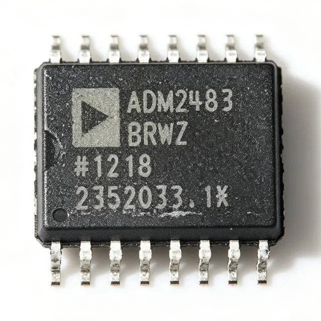
ADM2483BRWZ - Isolated RS-485 Transceiver | Analog Devices
The ADM2483BRWZ from Analog Devices is an integrated, galvanically isolated RS-485/RS-422 transceiver designed for bidirectional data communication on balanced, multipoint bus transmission lines. It combines a 3-channel digital isolator, a three-state differential line driver, and a differential input receiver into a single 16-pin SOIC package. The device complies with ANSI EIA/TIA-485-A and ISO 8482:1987 (E) standards, ensuring interoperability in industrial networks. With a data rate of 500 kbps and slew-limited driver outputs, it minimizes reflections and EMI in long cable runs. A digital isolator is a component that provides electrical isolation between two circuits while allowing digital signals to pass. It uses capacitive or magnetic coupling (such as Analog Devices' iCoupler technology) to transfer data across an isolation barrier, protecting sensitive logic from high voltages, ground loops, and noise. In the hierarchy of isolation components, a digital isolator falls under the category of isolation ICs, which are essential in industrial automation, motor control, and communication interfaces where safety and signal integrity are paramount. Key features of the ADM2483BRWZ include 2500 Vrms isolation voltage, 25 kV/µs common-mode transient immunity (CMTI), and a wide operating temperature range of -40°C to +85°C. The logic side can be powered with either 5 V or 3 V, while the bus side requires a 5 V supply. The device features a 3-channel configuration (one driver and two receiver channels) and supports half-duplex communication. Its low power consumption of 2.5 mA max makes it suitable for power-sensitive applications. Technically, the ADM2483BRWZ uses iCoupler technology, which employs chip-scale transformers to provide isolation, offering advantages over optocouplers in terms of speed, reliability, and power efficiency. The device includes thermal shutdown protection and is available in a 16-lead SOIC-W package with a standard 7.50 mm width. The slew-limited driver reduces electromagnetic interference, and the receiver has a wide common-mode input range, enhancing noise immunity. Typical applications include industrial fieldbus networks, PROFIBUS, Modbus, building automation, and HVAC systems. The device is ideal for isolating RS-485 buses in harsh environments where ground potential differences exist between nodes. Its high CMTI ensures reliable operation in the presence of fast transients, such as those from motor drives or lightning surges. When designing with the ADM2483BRWZ, ensure proper decoupling on both the logic and bus sides, and terminate the bus correctly to minimize reflections. The device is RoHS compliant and lead-free, making it suitable for environmentally conscious designs.

ADM2483BRWZ-RL7 - Isolated RS-485 Transceiver | Analog Devices
The ADM2483BRWZ-RL7 is a half-duplex, galvanically isolated RS-485 transceiver from Analog Devices, integrating a 3-channel digital isolator, a three-state differential line driver, and a differential input receiver in a single 16-lead SOIC-W package. It is designed for bidirectional data communication on balanced, multipoint bus transmission lines and complies with ANSI TIA/EIA RS-485-A-1998 and ISO 8482:1987(E). The device operates from a 5V or 3V logic supply (VDD1) and a 5V bus supply (VDD2), supporting data rates up to 500 kbps with slew-rate-limited driver outputs to minimize EMI. Key specifications include a 2500Vrms isolation rating, common-mode transient immunity greater than 25 kV/µs, and a low quiescent current of 2.5 mA maximum. The ADM2483BRWZ-RL7 is available in tape and reel packaging, making it suitable for high-volume production. An isolated RS-485 transceiver is a device that combines an RS-485 physical layer transceiver with galvanic isolation between the logic side and the bus side. It is a key component in industrial communication networks, where it provides a robust, noise-immune interface over long cable runs while protecting sensitive control electronics from ground potential differences, surges, and transients. The isolation barrier is typically implemented using capacitive or magnetic coupling, as in Analog Devices' iCoupler technology, which offers superior performance compared to optocoupler-based solutions in terms of speed, power consumption, and reliability. Key features of the ADM2483 include true fail-safe receiver inputs that guarantee a logic-high output when the bus is open, shorted, or idle, and chatter-free power-up/power-down protection that prevents spurious data during power cycling. The device supports up to 256 nodes on a bus, making it suitable for large multi-drop networks. Thermal shutdown protection prevents damage from excessive power dissipation. The wide operating temperature range of -40°C to +85°C ensures reliable operation in harsh industrial environments. Technically, the ADM2483 uses iCoupler technology, which employs chip-scale transformers to transmit data across the isolation barrier, providing high common-mode transient immunity and reliable operation at high data rates. The driver outputs are slew-rate limited to reduce radiated emissions, and the receiver has a wide common-mode input range of -7V to +12V, accommodating large ground potential differences. The device is available in a 16-lead SOIC-W package, which is compact and suitable for space-constrained designs. Typical applications include industrial fieldbus networks, building automation, HVAC systems, motor control, and remote data acquisition systems. The ADM2483 is ideal for applications requiring robust, isolated RS-485 communication over long distances, such as factory automation and process control. When designing with the ADM2483, it is important to provide proper decoupling on both VDD1 and VDD2, and to ensure that the bus termination resistors are correctly placed to match the cable impedance. The isolation barrier should be maintained with adequate creepage and clearance distances on the PCB to meet safety standards.
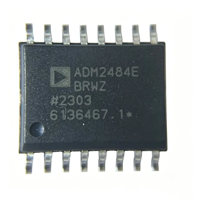
ADM2484EBRWZ - Isolated RS-485 Transceiver | Analog Devices
The ADM2484EBRWZ from Analog Devices is an isolated RS-485/RS-422 transceiver with integrated iCoupler digital isolation, providing 5000 Vrms isolation and ±15 kV ESD protection. It supports data rates up to 500 kbps and features a 25 kV/µs common-mode transient immunity (CMTI), making it suitable for industrial and instrumentation applications where robust communication over long distances is required. The device is available in a 16-lead SOIC package (0.295" width, 7.50 mm) and operates over a wide temperature range. An isolated RS-485 transceiver is a device that combines a differential line driver and receiver with galvanic isolation between the bus side and the logic side. This isolation protects the microcontroller and other low-voltage circuitry from ground potential differences, electrical noise, and transient surges that can occur on long communication lines. The ADM2484E integrates the isolation barrier using Analog Devices' iCoupler technology, which uses chip-scale transformers to transmit data across the isolation boundary, eliminating the need for external optocouplers and providing more reliable and higher-speed isolation compared to traditional optocoupler-based solutions. Key features of the ADM2484EBRWZ include a 3.3 V or 5 V logic supply, a 5 V bus supply, and a wide common-mode input range. The transceiver supports both half-duplex and full-duplex operation, with the transmitter outputs and receiver inputs sharing the same transmission line in half-duplex mode. The device also features thermal shutdown protection and a low quiescent current, making it suitable for power-sensitive applications. The ±15 kV ESD protection on the bus pins ensures robustness in harsh industrial environments. The ADM2484E uses a differential signaling scheme that provides excellent noise immunity and allows data transmission over distances up to 1200 meters. The integrated isolation barrier provides 5000 Vrms isolation, which is essential for applications where ground potential differences exist between nodes. The device's 25 kV/µs CMTI ensures that fast transients on the bus do not corrupt the data, making it ideal for motor drives, inverters, and other high-noise environments. Typical applications include industrial fieldbus networks, building automation, HVAC systems, and process control. The ADM2484EBRWZ is also suitable for isolated RS-485 interfaces in solar inverters, battery management systems, and other power electronics. Its robust ESD protection and high isolation voltage make it a reliable choice for long-distance communication in harsh environments. When designing with the ADM2484EBRWZ, it is important to provide proper decoupling on both the logic and bus supply pins, and to ensure that the bus termination resistors are correctly placed to match the characteristic impedance of the transmission line. The device's thermal shutdown feature protects it from over-temperature conditions, but adequate PCB layout with proper grounding is essential for optimal performance.
ADM2484EBRWZ-RL7 - Isolated RS-485 Transceiver | Analog Devices
The ADM2484EBRWZ-RL7 from Analog Devices is an isolated RS-485/RS-422 transceiver with integrated iCoupler digital isolation, providing 5000 Vrms galvanic isolation and ±15 kV ESD protection. It supports half- or full-duplex communication at data rates up to 500 kbps, making it ideal for industrial multipoint networks. The device operates from a 3.0 V to 5.5 V supply on the logic side (VDD1) and a 3.0 V to 3.6 V supply on the bus side (VDD2), with a common-mode transient immunity (CMTI) of 25 kV/µs. Housed in a 16-lead SOIC-W (0.295" width) package, it is available in tape and reel packaging (RL7 suffix). An isolated RS-485 transceiver is a device that combines a differential bus transceiver with galvanic isolation, typically using capacitive or magnetic coupling, to transmit data across a potential difference while preventing ground loops and protecting low-voltage logic from high-voltage transients. It sits within the hierarchy: isolated transceiver -> RS-485 transceiver -> interface IC -> semiconductor. This integration eliminates the need for external optocouplers and separate isolated power supplies, simplifying PCB design and improving reliability. Key features include 5000 Vrms isolation rating, 500 kbps data rate, 25 kV/µs CMTI, and ±15 kV ESD protection on the bus pins. The device also features thermal shutdown protection and a wide operating temperature range of -40°C to +125°C. The iCoupler technology ensures consistent timing and low power consumption, with a typical quiescent current of 2.5 mA on VDD1 and 2.0 mA on VDD2. Technically, the ADM2484E uses Analog Devices' iCoupler technology, which employs chip-scale transformers to isolate signals, providing superior performance compared to optocouplers in terms of speed, power, and reliability. The transceiver includes a differential driver and receiver, with the driver outputs Y and Z and receiver inputs A and B. For half-duplex operation, Y is tied to A and Z to B externally. The device also features a DE (driver enable) and RE (receiver enable) pins for bus control. Typical applications include industrial fieldbus networks, building automation, HVAC systems, and motor control drives, where robust communication over long distances and noisy environments is required. The high CMTI and ESD protection make it suitable for harsh industrial settings. When designing with this device, ensure proper decoupling on both VDD1 and VDD2 with 0.1 µF capacitors close to the pins. Also, terminate the bus properly (e.g., 120 Ω) to minimize reflections, and consider using a common-mode choke for enhanced EMI immunity.
ADM2486BRWZ - 20Mbps Isolated RS-485 Transceiver | Analog Devices
The ADM2486BRWZ from Analog Devices is a high-speed, half-duplex, galvanically isolated RS-485 transceiver that integrates a 3-channel digital isolator, a three-state differential line driver, and a differential input receiver in a single 16-lead SOIC package. It provides 2500Vrms isolation for 1 minute per UL 1577, with a common-mode transient immunity (CMTI) of 25kV/µs, ensuring robust data communication in electrically noisy industrial environments. The device supports data rates up to 20Mbps, making it suitable for high-speed multipoint bus applications. An isolated RS-485 transceiver is a component that combines an RS-485 physical layer interface with galvanic isolation, allowing data transmission between systems with different ground potentials while preventing harmful ground loops and common-mode voltage damage. It sits within the hierarchy: isolated RS-485 transceiver -> digital isolator + transceiver -> interface IC -> semiconductor. This integration reduces board space and improves reliability compared to discrete isolator plus transceiver solutions. Key features include a wide supply voltage range of 3V to 5.5V on the logic side and 5V on the bus side, a 20Mbps data rate, and a -7V to +12V common-mode input voltage range on the bus pins. The device also features thermal shutdown protection, a driver output short-circuit protection, and a receiver with true fail-safe inputs that guarantee a logic-high output when the bus is open, shorted, or idle. The 16-lead SOIC-16 package (7.50mm width) is industry-standard and supports surface-mount assembly. Technically, the ADM2486 uses Analog Devices' iCoupler technology, which employs chip-scale transformers to provide isolation, eliminating the need for optocouplers and their associated LED aging and current transfer ratio degradation. The device is fully specified over the industrial temperature range of -40°C to +85°C. Its high CMTI of 25kV/µs ensures reliable operation in the presence of fast transients, such as those from motor drives or power converters. Typical applications include industrial fieldbus networks, PROFIBUS, Modbus, building automation, and HVAC systems, where high-speed, isolated RS-485 communication is required. The ADM2486 is also used in motor control and power inverter systems to isolate the controller from the high-voltage bus side. When designing with this device, ensure proper PCB layout with adequate creepage and clearance distances for the isolation barrier, and place decoupling capacitors close to the VDD1 and VDD2 pins. The device requires a 5V supply on the bus side (VDD2) and can operate with 3.3V or 5V on the logic side (VDD1).
ADM2487EBRWZ - Isolated RS-485 Transceiver | Analog Devices
The ADM2487EBRWZ from Analog Devices is an isolated RS-485/RS-422 transceiver with an integrated transformer driver, providing 2.5 kVrms isolation and ±15 kV ESD protection. It supports data rates up to 500 kbps and features a common-mode transient immunity (CMTI) of 25 kV/µs, making it suitable for industrial multipoint communication networks. The device is configurable for half-duplex or full-duplex operation and comes in a 16-lead SOIC-W (0.295" width) package. An isolated RS-485 transceiver is a component that combines a differential line driver and receiver with galvanic isolation, allowing data transmission between systems with different ground potentials. It is a key element in industrial automation, building control, and instrumentation networks, where it ensures signal integrity and protects against ground loops and voltage transients. The ADM2487E belongs to the family of isolated interface ICs, which are part of the broader category of digital isolators and interface transceivers. Key features include an integrated oscillator driver for an external transformer, eliminating the need for a separate DC-DC converter, and a 3-channel architecture (one driver, one receiver, and one isolation channel). The device operates from a 5V supply on the logic side and a 5V supply on the bus side, with a typical quiescent current of 2.5 mA. It also features thermal shutdown and short-circuit protection on the driver outputs. The ADM2487E uses Analog Devices' iCoupler technology, which integrates micro-transformers to provide isolation, resulting in a compact and reliable solution compared to optocoupler-based designs. The high CMTI of 25 kV/µs ensures reliable operation in noisy industrial environments, and the ±15 kV ESD protection on the bus pins enhances robustness against electrostatic discharge. Typical applications include industrial fieldbus networks (PROFIBUS, Modbus), building automation (HVAC, lighting control), and instrumentation systems where long cable runs and ground potential differences are common. The device's half-duplex capability allows it to be used in 2-wire RS-485 networks, while full-duplex operation supports 4-wire configurations. When designing with the ADM2487E, ensure proper PCB layout with adequate spacing for isolation, and place the external transformer close to the device to minimize parasitic inductance. Also, terminate the bus properly to avoid reflections and ensure reliable communication at 500 kbps.
ADM2487EBRWZ-RL7 - Isolated RS-485 Transceiver | Analog Devices
The ADM2487EBRWZ-RL7 from Analog Devices is an isolated RS-485/RS-422 transceiver with integrated transformer driver, designed for high-speed, half-duplex or full-duplex communication on multipoint transmission lines. It provides 2500 Vrms isolation, ±15 kV ESD protection, and supports data rates up to 500 kbps. The device is housed in a 16-lead SOIC (0.295", 7.50mm width) package, suitable for industrial and instrumentation applications where galvanic isolation is required. An isolated RS-485 transceiver is a component that combines a differential line transceiver with galvanic isolation, allowing data communication between systems with different ground potentials. It integrates a digital isolator, a transceiver, and often a transformer driver to provide isolated power. This device belongs to the family of interface ICs, specifically digital isolators and bus transceivers, which are essential in industrial automation, building control, and medical equipment to prevent ground loops and protect against voltage transients. Key features include 2500 Vrms isolation voltage, 500 kbps data rate, 25 kV/µs common-mode transient immunity (CMTI), and ±15 kV ESD protection on the bus pins. The integrated oscillator driver allows the use of an external transformer to generate an isolated power supply, simplifying the design. The device supports both half-duplex and full-duplex configurations, with the transmitter outputs and receiver inputs sharing the same transmission line in half-duplex mode. Technically, the ADM2487E uses Analog Devices' iCoupler technology to provide isolation, which uses chip-scale transformers to couple signals across the isolation barrier. This results in reliable, high-speed data transfer with low power consumption. The device operates from a single 5V supply on the logic side and a 5V supply on the bus side, with a typical quiescent current of 2.5 mA. The bus pins are protected against ESD up to ±15 kV, ensuring robustness in harsh industrial environments. Typical applications include industrial fieldbus networks, building automation, HVAC systems, and isolated data acquisition systems. The device is particularly suited for applications requiring reliable communication over long distances (up to 1200 meters) and in noisy environments where galvanic isolation is critical. When designing with this device, ensure proper PCB layout to minimize parasitic capacitance across the isolation barrier. Use a suitable external transformer with the integrated driver to generate the isolated supply, and place decoupling capacitors close to the power pins. The device is RoHS compliant and available in tape and reel packaging.
ADM2490EBRWZ - Isolated RS-485 Transceiver | Analog Devices
The ADM2490EBRWZ from Analog Devices is a high-speed, ESD-protected, full-duplex, iCoupler isolated RS-485/RS-422 transceiver. It integrates a 2-channel digital isolator and a three-state differential line driver and receiver into a single 16-lead SOIC package, providing galvanic isolation up to 5000 Vrms. The device supports data rates up to 16 Mbps and offers ±8 kV ESD protection on the RS-485 input/output pins, making it suitable for industrial multipoint transmission lines. It complies with ANSI TIA/EIA-485-A-1998 and ISO 8482: 1987 (E) standards. An isolated RS-485 transceiver is a component that combines a differential bus transceiver with galvanic isolation, allowing data communication between systems with different ground potentials while preventing ground loops and protecting against common-mode voltage differences. It is a key building block in industrial automation, building control, and instrumentation networks, where robust and reliable data transmission over long distances is required. The isolation barrier is typically implemented using capacitive or magnetic coupling, as in Analog Devices' iCoupler technology. Key features of the ADM2490EBRWZ include a 16 Mbps data rate, 25 kV/µs common-mode transient immunity (CMTI), and a wide supply voltage range of 3.0 V to 5.5 V on the logic side and 5 V on the bus side. The device also features thermal shutdown protection and a three-state output for bus sharing. The iCoupler technology ensures low power consumption and high reliability compared to optocoupler-based solutions. The ADM2490E uses iCoupler technology, which employs chip-scale transformers to transmit data across the isolation barrier, offering superior performance in terms of speed, power efficiency, and reliability compared to traditional optocouplers. The device is designed for full-duplex communication, with separate differential driver and receiver pairs, and includes a driver enable pin for half-duplex operation. The wide operating temperature range of -40°C to +105°C makes it suitable for harsh industrial environments. Typical applications include industrial fieldbus networks, PROFIBUS, Modbus, building automation, and motor control systems. The high CMTI and ESD protection ensure reliable operation in noisy environments. The ADM2490EBRWZ is available in a 16-lead SOIC package (0.295" width, 7.50 mm) and is RoHS compliant. When designing with this device, ensure proper decoupling on both sides of the isolation barrier and consider the common-mode voltage range to avoid exceeding the device's specifications. The bus side should be terminated according to the transmission line impedance to minimize reflections.
ADM2490EBRWZ-RL7 - Isolated RS-485 Transceiver | Analog Devices
The ADM2490EBRWZ-RL7 is a high-speed, ESD-protected, full-duplex, iCoupler isolated RS-485 transceiver from Analog Devices. It integrates a two-channel digital isolator and a differential bus transceiver in a single 16-pin SOIC-W package, providing galvanic isolation up to 5000 Vrms. The device supports data rates up to 16 Mbps and features a high common-mode transient immunity (CMTI) of 25 kV/µs, ensuring reliable communication in electrically noisy environments. An RS-485 transceiver is a device that converts logic-level signals to differential voltages for balanced data transmission over twisted-pair cables, enabling robust communication over long distances and in harsh industrial settings. The ADM2490E belongs to the family of isolated interface ICs, which combine signal isolation and line driving in one package, simplifying PCB design and improving system reliability. Key features include a 5V supply on both logic and bus sides, a full-duplex interface with separate driver and receiver channels, and thermal shutdown protection. The device is specified for operation over the industrial temperature range of -40°C to +105°C. Its integrated iCoupler technology uses chip-scale transformers to provide isolation, eliminating the need for external optocouplers and associated components. The ADM2490E is designed for multipoint bus transmission, allowing up to 64 nodes on a single bus. It includes a receiver with a wide common-mode input range and a driver with short-circuit protection. The device is fully compliant with TIA/EIA RS-485 and RS-422 standards, making it suitable for industrial automation, building control, and instrumentation networks. Typical applications include industrial fieldbus systems, HVAC control networks, and isolated data acquisition systems. The high CMTI and 5000 Vrms isolation make it ideal for applications requiring robust galvanic isolation, such as motor drives and power inverters. When designing with this device, ensure proper PCB layout with adequate creepage and clearance distances for the isolation barrier. Place decoupling capacitors close to the supply pins and use a solid ground plane to minimize noise coupling.