Power Management
ژێرپۆلەکان
بەرهەمەکان (2,800+)

TPS6287B20VA0WRZVR - 20A Sync Buck Converter | Texas Instruments
The Texas Instruments TPS6287B20VA0WRZVR is a 20A synchronous step-down DC/DC buck converter with I2C interface and differential remote sense, operating from a 2.7V to 6V input and delivering a programmable 0.4V to 1.675V output in a 24-pin WQFN (RZV) package with exposed pad. A buck (step-down) converter is a switching voltage regulator that efficiently reduces a higher DC input voltage to a lower, tightly regulated output voltage using high-frequency switching of integrated power MOSFETs together with an inductor and capacitors. Within the power-management IC hierarchy, it belongs to the family of switching regulators, which achieve far higher efficiency than linear regulators (LDOs), making them the default choice for high-current point-of-load supplies in modern digital systems. Key features include a pin-to-pin compatible current family spanning 10A (TPS6287B10), 15A (B15), 20A (B20), 25A (B25) and 30A (B30), three selectable output voltage ranges with output resolution down to 1.25mV steps, low-resistance integrated power switches for high efficiency at high ambient temperature, and stacking support in parallel mode for even higher output currents. The TPS6287B20 architecture emphasizes fast transient response: it is specified as a fast-transient synchronous converter, allowing tight voltage regulation on dynamically loading rails such as processor cores and FPGAs. The I2C interface enables output voltage programming, telemetry, and status monitoring, while the differential remote sense input compensates for PCB voltage drop at the point of load. Frequency synchronization is also supported, simplifying multi-rail EMI management. Typical applications include powering high-current SoC and FPGA core rails, network processors and switch ASICs, data-center storage and server point-of-load supplies, and stacking multiple devices for 40A-plus rails in AI accelerators and high-performance computing. Design consideration: because this is a high-current buck regulator, inductor selection, switch-node layout, and thermal copper area dominate performance - follow the Texas Instruments datasheet layout guidelines closely to minimize switching losses and board-level temperature rise. This page synthesizes distributor pricing, pin-to-pin family alternatives, drop-in options, and practical design notes not found in the manufacturer datasheet alone.

TPS63000DRCR - 1.8A Buck-Boost Converter | Texas Instruments
The Texas Instruments TPS63000DRCR is a high-efficiency buck-boost converter with 1.8A current switches housed in a 10-pin VSON (DRC) package measuring 3 mm x 3 mm. It operates from a 1.8V to 5.5V input and delivers an adjustable output from 1.2V to 5.5V at up to 1.6A switch current, supporting products powered by two-cell or three-cell alkaline, NiCd, or NiMH batteries, or by a single-cell Li-ion/Li-polymer battery. The device reaches up to 96% efficiency, addressing conversion loss in portable applications where battery life and thermal budget are tightly constrained. A buck-boost converter is a switched-mode DC-DC topology that seamlessly transitions between buck (step-down), boost (step-up), and buck-boost operation as the input voltage crosses the regulated output setpoint. Within the broader power management IC hierarchy, it sits above simple LDOs and single-mode buck converters, since it must maintain regulation when VIN is below, equal to, or above VOUT. This makes buck-boost ICs essential for battery-powered systems whose rail voltage crosses a fixed output during discharge, and it gives them a unique role above linear regulators in efficiency, and alongside but functionally distinct from standalone buck or boost converters. Key features of the TPS63000 include a 1.5 MHz fixed switching frequency that permits the use of small inductors and ceramic capacitors, an adaptive hysteresis-based PWM/PFM control that maximizes efficiency across the full load range, and a power-save mode that drops quiescent current substantially at light loads. The device also offers a low-battery warning comparator, an enable input for power sequencing, and built-in thermal shutdown. The QFN-10 (3 mm x 3 mm) package with an exposed thermal pad delivers low parasitic inductance and adequate thermal performance for the converter's continuous 1.6A switch current. The TPS63000 uses TI's proprietary control scheme, described in the manufacturer datasheet, that adjusts duty cycle and switching behavior automatically based on the input-to-output voltage ratio. At 3.3V VIN and 3.3V VOUT the device runs at approximately 95% efficiency at moderate loads, while at 2V VIN (near end-of-discharge of a Li-ion cell) the boost region still maintains roughly 90% efficiency. The exposed thermal pad enables direct PCB heat spreading, which keeps junction temperature rise manageable without an external heatsink. Typical applications include portable media players, handhelds and portable terminals, industrial metering, single-cell Li-ion powered equipment, two-cell alkaline or NiMH powered systems, sensor modules and low-power wireless data acquisition, and any system whose battery voltage range straddles the regulated output voltage. The wide VIN window and adjustable VOUT also suit USB peripherals that must operate at 3.3V from a 4.5V to 5.5V rail. When designing with this converter, pay close attention to inductor selection (a 1.5 uH to 2.2 uH shielded inductor is typically recommended) and ensure the input/output ceramic capacitors meet the minimum value and voltage derating requirements described in the manufacturer datasheet. Place both capacitors as close as possible to the IC pins and use a continuous ground plane under the exposed pad to minimize EMI and ensure proper thermal dissipation. This page synthesizes distributor pricing, drop-in alternatives, and practical design notes not found in the manufacturer datasheet, providing engineering context for the TPS63000DRCR beyond the datasheet alone.
TPS63021 - 4A Switch Buck-Boost Converter | Texas Instruments
The Texas Instruments TPS63021 is a high-efficiency, single-inductor buck-boost converter with 4A switches, designed to provide a regulated output voltage from input sources that can be above or below the output. It supports output currents up to 3A and is available in a 14-pin VFDFN (DSJ) package with exposed thermal pad. The device operates from input voltages ranging from 1.8V to 5.5V, making it suitable for battery-powered applications using two or three alkaline, NiCd, or NiMH cells, or a single Li-ion or Li-polymer cell. A buck-boost converter is a type of DC-DC converter that can step up (boost) or step down (buck) the input voltage to maintain a constant output voltage, regardless of whether the input is higher or lower than the output. This is essential in battery-powered systems where the battery voltage declines over time, falling below the required rail voltage. The TPS63021 belongs to the power management IC family, specifically within DC-DC converters, and is a key component in portable electronics. Key features include a fixed 3.3V output voltage, high efficiency up to 96%, and a low quiescent current of 50 µA. The device integrates synchronous rectification, which eliminates the need for an external Schottky diode, improving efficiency and reducing component count. It also features load disconnect, light-load efficiency, and undervoltage lockout (UVLO) with fixed thresholds. The TPS63021 operates over a junction temperature range of -40°C to +125°C. Technically, the TPS63021 uses a proprietary control architecture that seamlessly transitions between buck and boost modes, ensuring stable output voltage with minimal ripple. The 4A switches allow for high output currents, and the device can deliver up to 3A in boost mode from a 3.3V input. The VFDFN package with exposed pad provides excellent thermal performance, with a thermal resistance of 40°C/W, enabling compact designs without external heatsinks. Typical applications include portable electronics, battery-powered devices, and systems powered by supercapacitors. The TPS63021 is ideal for powering microcontrollers, sensors, and wireless modules in IoT devices, where input voltage varies widely. Its high efficiency extends battery life, and its small footprint saves board space. When designing with the TPS63021, ensure proper input and output capacitor selection to minimize ripple and maintain stability. Use low-ESR ceramic capacitors with sufficient voltage rating. The exposed pad must be soldered to a thermal land on the PCB for optimal heat dissipation.
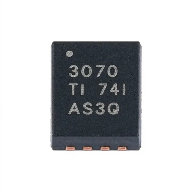
TPS63070RNMT - 2V-16V, 2A Buck-Boost Converter | TI
The Texas Instruments TPS63070RNMT is a high-efficiency, wide-input buck-boost DC-DC switching regulator that maintains a regulated output whether the input is above or below the target. It operates from 2V to 16V input, delivers up to 2A output current, and provides an adjustable output of 2.5V to 9V in a compact 15-pin VQFN-HR (RNM) package with -40C to +125C junction operation. A buck-boost converter is a type of DC-DC switching regulator within the broader power management IC category that combines buck (step-down) and boost (step-up) topologies. This lets a single inductor-based stage produce a stable rail from sources such as 4-cell alkaline, 12V lead-acid, or solar inputs whose voltage swings across the output level. The TPS63070 belongs to the switching voltage regulator family used in portable, industrial, and IoT power systems. Key features include a 3.6A switch current limit, 2.4MHz switching frequency, and low quiescent current of approximately 50uA typical. Synchronous rectification with integrated MOSFETs improves efficiency and reduces external component count, while the 2.4MHz clock permits small inductors and capacitors for a compact footprint. PWM mode maximizes heavy-load efficiency and PFM mode preserves light-load efficiency; the device also supports negative output current sinking in PWM mode per TI datasheet SLVSDD7B. Architecture-wise, the four-switch synchronous buck-boost topology seamlessly transitions between buck, buck-boost, and boost operating regions with a single inductor, avoiding output discontinuity when the battery voltage crosses the setpoint. The adjustable feedback (FB) pin sets the output with a resistor divider, and programmable soft-start limits inrush current. Typical applications include battery-powered portable instruments, industrial sensors, IoT wireless nodes, and 12V rail conditioning for microcontrollers, RF modules, and displays. Wide input tolerance makes it ideal for solar or vehicle-supplied systems. For best results, keep the inductor and input/output capacitor loops short, place the input capacitor at VIN and PGND, and provide adequate copper on the thermal pad. Pricing references are as of 2026-08-28.
TPS63710 - 1A Low Noise Inverting Buck Converter | TI
The Texas Instruments TPS63710 (TPS63710DRRR) is a low-noise synchronous inverting buck converter that generates a negative output voltage down to -5.5 V from a positive input of 3.1 V to 14 V, delivering up to 1 A of output current depending on the input-to-output voltage ratio. It is packaged in a 3-mm x 3-mm 12-pin WSON with exposed pad (12-WFDFN), providing excellent thermal performance for space-constrained designs. An inverting buck converter is a type of DC-DC switching regulator that produces a negative output rail from a positive supply. It belongs to the broader family of switching voltage regulators within power management ICs, which convert and regulate voltages efficiently using inductive energy storage rather than the dissipative approach of linear regulators. This makes inverting buck converters well suited to battery-powered and higher-current negative-rail applications where charge pumps cannot supply enough current. Key features of the TPS63710 include a filtered reference system with an external capacitor on the CAP pin that suppresses low-frequency 1/f noise up to approximately 100 kHz, a performance level required in high-performance telecommunication systems. The fixed-frequency PWM control topology gives predictable switching behavior and simple EMI filtering. Synchronous rectification eliminates the external Schottky diode, improving efficiency and reducing bill-of-material count. An enable pin supports power sequencing, and integrated soft-start limits inrush current. The device targets applications requiring a clean negative rail, such as op-amp supply rails, data converters, RF transceivers, bias supplies for GaN amplifiers, and optical modules. Its low-noise reference system makes it suitable for powering sensitive analog circuitry where output ripple and noise degrade signal integrity, while the wide input range supports both 5 V and 12 V system rails. When designing with the TPS63710, select input and output capacitors and an inductor with adequate saturation current to maintain stability and handle peak currents, and solder the exposed thermal pad to a copper area for heat dissipation. As of 2026-08-29, single-unit pricing from distributors starts near $1.51 (LCSC), with stock available at DigiKey, Mouser, and LCSC.
TPS63710DRRR - 1A Low-Noise Inverting Buck Converter | TI
The Texas Instruments TPS63710DRRR is a low-noise synchronous inverting buck converter that generates a negative output voltage down to -5.5 V from a positive input of 3.1 V to 14 V, delivering up to 1 A of load current depending on the input-to-output voltage ratio. It is housed in a 12-pin WSON package with an exposed thermal pad (12-WFDFN, 3 mm x 3 mm) that provides low thermal resistance for compact, high-density designs. An inverting buck converter is a type of DC-DC switching regulator that produces a negative output rail from a positive supply rail. It belongs to the broader family of switching voltage regulators within power management ICs, which convert and regulate voltages efficiently using inductive energy storage rather than the dissipative approach of linear regulators. This makes inverting buck converters well suited to battery-powered and higher-current negative-rail applications where simple charge pumps cannot supply enough current and where LDO efficiency would be unacceptable. Key features of the TPS63710 include a filtered reference system with an external capacitor on the CAP pin that suppresses low-frequency 1/f noise up to approximately 100 kHz - a noise performance required in high-performance telecommunication systems. The fixed-frequency PWM control topology gives predictable switching behavior and simplifies EMI filtering. Synchronous rectification eliminates the need for an external Schottky diode, improving efficiency and reducing bill-of-material count. An enable pin supports power sequencing, and integrated soft-start limits inrush current at startup. The device targets applications requiring a clean negative rail such as op-amp supply rails, data converters, RF transceivers, bias supplies for GaN amplifiers, and optical modules. Its low-noise reference system makes it well suited to powering sensitive analog circuitry where output ripple and noise would otherwise degrade signal integrity, while the wide 3.1 V to 14 V input range supports both 5 V and 12 V system rails. When designing with the TPS63710, choose input and output capacitors plus an inductor with adequate saturation current to maintain stability and handle peak currents, and solder the exposed thermal pad to a copper area for heat dissipation. As of 2026-10-11, single-unit pricing from distributors starts near $1.51 (LCSC), with stock available at DigiKey, Mouser, and LCSC. This page synthesizes distributor pricing, drop-in alternatives, and practical design notes not found in the manufacturer datasheet.
TPS63900DSKR - 400mA 75nA IQ Buck-Boost DVS Converter | Texas Instruments
The Texas Instruments TPS63900DSKR is a four-switch synchronous buck-boost converter with 400 mA maximum output current, an ultra-low 75 nA quiescent current, and 32 user-programmable output voltage settings from 1.8 V to 5 V, housed in a 10-pin WSON (DSK) exposed-pad package. It accepts an input voltage range of 1.8 V to 5.5 V and integrates an adjustable input current limit plus Dynamic Voltage Scaling (DVS), which lets the host step the output between two preloaded voltages during operation. A buck-boost DC-DC converter is a switching regulator topology that maintains a regulated output voltage whether the input voltage sits above, below, or equal to the output. Unlike a buck (step-down only) or boost (step-up only) regulator, the buck-boost uses four switches to seamlessly transition between modes, eliminating output-voltage transients during the mode boundary. Within the power management hierarchy, the TPS63900 belongs to the broader family of switching regulators (DC-DC converters) that also includes LDOs, charge pumps, and PMICs. Its 75 nA quiescent current makes it a member of the nano-IQ class favored by battery-powered IoT designs. Key differentiating features include single-mode operation that avoids the mode-switching transients and unpredictable inductor current ripple seen in many competing buck-boost parts, 32 selectable output voltages stored in a one-time-programmable (OTP) memory, true shutdown with 5 nA Iq, and an exposed thermal pad that lowers junction-to-ambient thermal resistance. The DVS pin toggles between two programmed Vout levels without software reload delay, an advantage for systems that must reduce the rail during sleep. Architecturally, the TPS63900 uses a peak-current-mode control loop with synchronous rectification. A single 1-µH inductor handles all four switching phases, reducing BOM cost. The internal MOSFETs are rated for the full 1.8-5.5 V input range, and the adjustable input current limit lets designers protect weak source batteries such as coin cells or energy harvesters. Typical applications include battery-powered IoT nodes, wearables, energy-harvesting sensor platforms, BLE/Zigbee radio power rails, ultra-low-power MCUs, and backup-power systems where the converter must hold regulation across a wide Vin swing. The combination of nano-Iq, DVS, and OTP-programmable outputs is especially well suited to designs that spend most of their life in standby and burst-transmit at higher loads. When designing with this part, follow the datasheet's recommended 1 µH inductor with low DCR (< 50 mΩ) and place the four ceramic bypass capacitors (2x 10 µF input + 2x 10 µF output minimum) within 2 mm of the package. Check the worst-case thermals at the maximum 400 mA load, since the WSON-10 package relies on PCB copper for heat spreading. This page synthesizes XAIPART distributor pricing, drop-in alternatives sourced from TI cross-reference data and same-family parametric memory, and practical design notes that go beyond the manufacturer datasheet to accelerate your selection.
TPS650362-Q1 - Automotive 35V PMIC | Texas Instruments
The TPS650362-Q1 is a highly integrated automotive power management IC (PMIC) from Texas Instruments, designed for camera and radar modules and MCU power in automotive systems. It combines three step-down (buck) converters and one low-dropout (LDO) regulator in a single device, with the BUCK1 input voltage range capable of supporting up to 35V, enabling direct connection to automotive 12V/24V battery rails. The device is qualified for automotive applications up to ASIL-B functional safety level, making it suitable for ADAS and autonomous driving systems. A PMIC (Power Management IC) is a form of integrated circuit that manages the power requirements of a host system, providing multiple regulated voltages from a single input source. The TPS650362-Q1 fits into the power management hierarchy as a highly integrated PMIC → automotive power management IC → automotive semiconductor, consolidating multiple discrete regulators into one solution to reduce board space, cost, and system complexity. Key features include three independent buck converters for high-efficiency step-down conversion, one LDO for noise-sensitive analog rails, and an input voltage capability of 35V on BUCK1. The device's ASIL-B capability supports functional safety requirements in automotive safety-critical systems. Its integrated architecture reduces external component count and enables a compact camera module design. In terms of technical depth, the TPS650362-Q1 utilizes TI's advanced process technology to combine high-voltage input capabilities with efficient switching converters. The buck converters likely operate at high switching frequencies to minimize magnetic component sizes, while the LDO provides low-noise output for sensitive analog circuits. The device is designed to meet stringent automotive reliability standards. Typical applications for the TPS650362-Q1 include automotive camera modules, radar systems, and MCU power supplies. Its 35V input capability allows direct connection to filtered 12V automotive power, while ASIL-B qualification makes it suitable for safety-relevant functions. When designing with this PMIC, ensure proper input decoupling for the high-voltage buck converter and follow recommended layout practices to minimize switching noise. Verify the complete pinout and package specifications from the official datasheet before production.

TPS65036x-Q1 - Automotive PMIC | Texas Instruments
The TPS65036x-Q1 is a highly integrated automotive power management IC (PMIC) from Texas Instruments, designed for camera, radar, and MCU power systems. It combines three step-down (buck) converters and one low-dropout (LDO) regulator in a compact 24-pin VQFN package (3.5mm × 3.5mm), delivering robust, efficient power for ADAS applications. What is a PMIC? A Power Management IC integrates multiple power conversion and regulation functions, such as voltage regulators, LDOs, and battery management, into a single chip. PMICs are essential in automotive electronics to generate the various supply rails required by processors, sensors, and peripherals from a single battery input, reducing board space, cost, and complexity. The TPS65036x-Q1 sits in the power management hierarchy, specifically in the automotive camera/radar/MCU power sub-system. Key features include a wide-input-voltage BUCK1 converter supporting up to 35V, allowing direct connection to automotive 12V/24V battery systems. Two additional low-voltage buck converters and a 300mA LDO provide multiple rails. The device supports forced fixed-frequency PWM mode or AutoPFM mode for efficiency across load ranges, optional spread-spectrum modulation for EMI reduction, and low-power operation controlled via pin or I2C. The TPS65036x-Q1 is AEC-Q100 qualified for automotive reliability, with an operating temperature range up to +125°C. The integrated sequencing and I2C interface enable flexible power management and diagnostics. The 24-pin VQFN package with a 0.5mm pitch and 3.5x3.5mm footprint minimizes PCB area, critical in space-constrained camera modules. Typical applications include automotive camera modules, radar units, and MCU power supplies in ADAS systems, where multiple regulated rails are needed from a single automotive battery. The device also supports infotainment and sensor fusion systems requiring low-noise, reliable power. When designing with the TPS65036x-Q1, pay attention to thermal management: the buck converters and LDO can dissipate significant power at high input voltages and load currents. Ensure adequate copper pour and thermal vias to keep junction temperatures within limits. Also, properly configure the I2C address and default settings for your specific application variant.

TPS65216D0RSLR PMIC for ARM Cortex-A8/A9 SOCs | TI VQFN-48
The Texas Instruments TPS65216D0RSLR is an integrated power management IC (PMIC) purpose-built for ARM Cortex-A8/A9 application processors and FPGA systems, housed in a 48-pin VQFN (RSL) package measuring 6 mm × 6 mm with a 0.4 mm pitch. The device operates from a 3.6 V to 5.5 V input rail, integrating multiple buck converters and LDOs to deliver the complete power tree required by Sitara AMIC110/AMIC120 and other Cortex-A series SOCs in a single chip. A PMIC (Power Management Integrated Circuit) is a mixed-signal IC that combines multiple DC-DC converters, LDOs, sequencers, voltage monitors, and supervisory logic into one package. Within the broader taxonomy, a PMIC belongs to the power management semiconductor category, which itself falls under analogue and mixed-signal ICs. Modern PMICs are essential for systems-on-chip designs because they shrink the power-section footprint, reduce quiescent losses and guarantee deterministic rail sequencing during power-up, power-down and fault events. Key features of the TPS65216 include up to three step-down DC-DC converters (each up to 2 A peak), two LDOs, power-good / reset logic, and programmable output voltages set by I2C or external feedback resistors. The wide 3.6 V to 5.5 V input range allows the device to run directly from a single-cell Li-ion battery, a 5 V USB rail or a regulated intermediate bus. The 48-pin VQFN package includes an exposed thermal pad to keep the junction temperature under control when the converters deliver full output current. Architecturally, the TPS65216D0 (the D0 silicon revision) integrates a synchronous buck topology with internal MOSFETs and uses an internal bandgap reference plus per-rail feedback to hit output accuracies within a few percent. Built-in protection such as over-current, over-temperature, and under-voltage lockout makes it robust for industrial and consumer SBC designs. The PMIC also supports DDR-memory power requirements, including the VPP and VTT rails demanded by LPDDR/DDR memories paired with the host processor. Typical applications include industrial automation controllers, Sitara AM335x/AM437x SBCs, FPGA-based vision and motor-control boards, and portable ARM-based test instruments. The wide input range and integrated sequencing make it especially valuable in any design where the system must start cleanly on a single lithium cell while still powering a multi-rail processor. A key design consideration is decoupling: place a 1 µF ceramic input capacitor and per-output ceramic capacitors as close as possible to the device pins to keep ripple below the level visible to the host SOC. Always tie the exposed pad to a continuous ground plane for thermal relief, especially when drawing full converter current. This page synthesises distributor pricing, drop-in alternative coverage, and practical design notes that complement the TI datasheet with application-level engineering context.
TPS652170RSLT - PMIC for AM335x w/ 3 DC/DCs, 4 LDOs, Charger | TI
The Texas Instruments TPS652170RSLT is a single-chip, user-programmable power management IC (PMIC) designed to power the AM335x ARM Cortex-A8 processor in portable and 5-V line-powered applications. The device integrates three step-down converters (DC/DCs), four low-dropout (LDO) regulators, a linear single-cell Li-ion/Li-polymer battery charger, a dual-input power path, and an LED driver inside a 48-pin VQFN (RSL) 6x6 mm package. A PMIC (Power Management Integrated Circuit) is a category of voltage regulator and battery management IC that consolidates multiple power rails, sequencing logic, monitoring, and protection into one device. PMICs sit in the power management hierarchy between the system battery or adapter and the application processor, providing tightly coordinated, compact, and efficient power for SoCs (system-on-chip), FPGAs, and microcontrollers. The TPS652170's three step-down converters each deliver up to 1.5 A continuous output current at output voltages programmable from 0.6 V to VIN, supporting the AM335x core, DDR memory, and I/O rails. The four LDOs cover analog, PLL, and housekeeping supplies, while the integrated linear charger supports single-cell Li-ion/Li-polymer packs with thermal regulation and JEITA-style protection. A high-efficiency boost converter is also integrated to supply LED strings or auxiliary rails. The user-programmable NVM (non-volatile memory) configuration via I2C lets the design engineer define default output voltages, sequencing, and protection thresholds. Typical applications include AM335x-based Sitara industrial HMI panels, portable data terminals, IoT gateways, e-readers, point-of-sale terminals, and any portable or 5-V line-powered product that requires a compact, multi-rail power solution with battery charging. When designing with this device, allocate sufficient PCB copper under the exposed thermal pad (EP) for heat spreading; the VQFN-48 RSL package uses the EP as the primary thermal path. Observe the I2C address selection (0x24 / 0x25) and the GPIO sequencing pins for multi-PMIC coordination. This page synthesizes TI datasheet specifications, distributor pricing, drop-in package-compatible alternatives, and practical design notes not aggregated elsewhere.
TPS65217CRSLR - Single-Chip PMIC for AM335x ARM Cortex-A8 | Texas Instruments
The Texas Instruments TPS65217CRSLR is a single-chip power management IC (PMIC) specifically designed to power the AM335x ARM Cortex-A8 microprocessor in portable and 5-V line-powered applications, integrating 3 step-down DC/DC converters, 4 low-dropout (LDO) regulators, a linear Li-ion/Li-polymer battery charger, dual-input power path management, and a high-efficiency white-LED boost driver, all in a 48-pin VQFN (RSL) 6x6 mm package with 0.4 mm pitch. The device operates over an ambient temperature range of -40C to +105C, supports an input voltage up to 5.5 V from USB, AC adapters, or battery sources, and provides sequenced power rails with I2C control and status indication. The RSL suffix denotes the 48-pin leadless package, while the production-grade operating range and feature set make the part well suited to industrial handheld designs, point-of-sale terminals, and consumer mobile devices based on the TI Sitara AM335x platform. A PMIC (Power Management Integrated Circuit) is a single silicon device that consolidates multiple voltage regulators, battery management functions, and often ancillary drivers (LED, USB, RTC) into one package. Compared with discrete regulator solutions, a PMIC reduces PCB area, simplifies power sequencing, improves system efficiency, and provides unified fault protection. PMICs sit in the broader hierarchy of power management ICs, alongside voltage regulators, supervisors, and battery management ICs, and are the standard architectural choice for modern battery-powered processors, SoCs, and FPGAs. Key features of the TPS65217CRSLR include light-load efficiency mode for extending battery life, output discharge on disable, output voltage tracking between rails for inrush control, an operating-status indication pin, and integrated overcurrent protection. Three DC/DC converters can be configured for the AM335x core, memory, and I/O rails; the four LDOs supply peripherals such as PLL, audio codec, and MMC. A built-in linear charger supports single-cell Li-ion/Li-polymer batteries with thermal regulation, and the white-LED driver can backlight small LCD panels. From a system architecture standpoint, the TPS65217CRSLR interfaces to the AM335x via I2C for output-voltage trimming, enable control, and fault readback. Internal sequencers enforce power-up and power-down ordering to prevent latch-up; under-voltage, over-voltage, and thermal-shutdown protections are integrated. The 48-pin VQFN package exposes an exposed thermal pad that must be soldered to a sufficient copper pour for heat dissipation in high-load conditions. Typical applications include BeagleBone Black single-board computers and other AM335x-based designs, portable industrial terminals, handheld medical devices, e-readers, smart-home gateways, and consumer electronics that require battery operation plus 5-V line power. Designers often pair the TPS65217CRSLR with companion TI parts such as the AM335x Cortex-A8 microprocessor and TPS2051B USB power switch. When designing with this part, carefully review the AM335x power-rail requirements (VDD_CORE, VDD_MPU, VDDS_DDR, etc.) and configure the DC/DCs and LDOs accordingly. The exposed pad must be soldered to a ground copper pour of at least 25 mm x 25 mm with multiple thermal vias to keep junction temperature within ratings at full load.
TPS65217CRSLT - Single-Chip PMIC for AM335x | Texas Instruments
The Texas Instruments TPS65217CRSLT is a single-chip Power Management IC (PMIC) that integrates three step-down DC/DC converters, four low-dropout (LDO) regulators, a linear Li-ion/Li-polymer battery charger, a dual-input power path (USB/AC), and a white LED boost driver in a 48-pin VQFN (6x6 mm) package. It is specifically designed to power the AM335x ARM Cortex-A8 application processor in portable and 5-V line-powered systems, and operates from an input range of 4.3 V to 5.8 V with 2.25 MHz switching frequency. A PMIC (Power Management Integrated Circuit) is a highly integrated device that consolidates multiple voltage rails, charging, sequencing, and supervisory functions into a single silicon die. In the system hierarchy, it sits between the input power source (battery or wall adapter) and the application processor, replacing what would otherwise be 5-10 discrete regulators. PMICs are essential in space-constrained portable designs such as tablets, handhelds, and embedded modules where board area, BOM count, and power-sequencing reliability are critical design constraints. The TPS65217CRSLT supports 2-A output current on the linear charger power path with a 700-mA maximum charge current, 20-V tolerant USB and AC inputs, and an 1800-mA current limit option on the USB input. Thermal regulation, dynamic power-path management, and integrated power-good signaling simplify host-side firmware. The high-frequency 2.25-MHz switching converters enable the use of small 1-uH inductors and 0402/0603 ceramic capacitors, reducing total PCB footprint. Architecturally, the device combines hysteretic and PWM buck controllers for high efficiency across load, low-Iq LDOs for always-on rails, and a current-mode linear charger with JEITA-style thermal regulation. The integrated boost converter drives white LEDs for display backlighting with software-controllable brightness. According to the TI datasheet PDF, the TPS65217x family is shipped in a 48-pin leadless 6-mm x 6-mm VQFN package with 0.4-mm pitch, and is qualified for industrial temperature ranges. Typical applications include AM335x-based Sitara processor boards (BeagleBone Black, industrial HMI panels), portable medical data-acquisition tablets, handheld barcode scanners, e-readers, and ruggedized 5-V point-of-sale terminals. The wide 4.3-5.8-V input range makes it directly compatible with USB 2.0/3.0 VBUS rails, single-cell Li-ion batteries, and 5-V regulated adapters without additional front-end conditioning. When designing with the TPS65217CRSLT, place the input bulk capacitors as close as possible to the PVIN and PGND pins to minimize parasitic inductance. Use a 4-layer PCB with a dedicated ground plane for best thermal performance at 2-A charging current. Refer to the TI TPS65217EVM evaluation module schematic for reference layout, recommended inductor selection, and proper power-good pull-up configuration. This page synthesizes distributor pricing, AM335x-focused drop-in alternatives, and PCB layout notes drawn from TI reference designs - engineering context not aggregated on any single manufacturer page.

TPS6521855 - 7-Output PMIC for AM64x | Texas Instruments
The Texas Instruments TPS6521855 is a single-chip Power Management IC (PMIC) specifically designed to support the AM64x line of Sitara Arm Cortex-A53 processors. It delivers seven regulated output rails in a 48-pin VQFN (6x6 mm) surface-mount package and supports both portable Li-Ion battery and nonportable 5V adapter input topologies. The device is characterized across a -40C to +105C industrial temperature range. A Power Management IC (PMIC) is a highly integrated device that consolidates multiple power conversion functions - DC-DC converters, LDO regulators, power sequencing, voltage monitoring, and protection - into one package. In processor-based systems, the PMIC sits between the power source and the SoC's multiple voltage domains, translating a battery or adapter input into the core, memory, I/O, and auxiliary rails. Within the system hierarchy, a PMIC belongs to the power management IC family, and its role is to provide reliable, sequence-correct power delivery at every boot and operating state. Key features include seven integrated output channels, factory pre-programmed default register settings matched to the AM64x power-up sequence, and an input voltage range of 2.2V to 5.5V with output voltages configurable from 0.85V to 3.4V at up to 1.8A per the distributor-listed output current. The factory configuration reduces firmware bring-up effort because the device starts with AM64x-compatible settings without external programming. From an architecture perspective, the TPS6521855 is closely related to the TPS6521815 in the TPS65218 family. According to a TI E2E power-management forum discussion, TPS6521815 and TPS6521855 are pin-to-pin compatible devices sharing the same programming steps; the TPS6521855 ships pre-programmed for AM64x, while the TPS6521815 is configured via register programming for custom sequencing. Typical applications include industrial PLCs and factory automation controllers, portable battery-powered instruments, IoT edge gateways, robotics and motion-control boards, and test-and-measurement instrumentation. In each case, the AM64x multi-rail power requirements are met by a single 48-VQFN PMIC, reducing BOM count and board area. When designing, verify the input source configuration (Li-Ion vs 5V adapter) and place adequate input and output capacitance close to the package. If sequencing different from factory defaults is required, select the TPS6521815 and program the register map accordingly.

TPS65218B1PHPR - 7-Output PMIC for ARM Cortex-A8/A9 SoC | TI
The Texas Instruments TPS65218B1PHPR is a power management IC (PMIC) designed for ARM Cortex-A8/A9 SoCs and FPGAs, integrating 7 regulator outputs in a 48-pin HTQFP (7x7) package with exposed thermal pad. It operates from a 2.7V to 5.5V input supply and supports a -40C to +105C industrial temperature range, making it suitable for embedded computing platforms with multiple voltage domains. A PMIC (Power Management IC) is a highly-integrated device that consolidates multiple DC-DC converters, LDOs, and supervisory functions into a single package. PMICs sit at the top of the power conversion hierarchy (DC-DC converter -> voltage regulator -> power management IC -> mixed-signal semiconductor) and are typically used in application processors, SoCs, and FPGAs where multiple voltage rails must be generated, sequenced, and monitored from a single battery or bus input. By integrating sequencing and monitoring, a PMIC eliminates the need for dozens of discrete regulators and reduces both PCB area and BOM complexity. Key features of the TPS65218B1PHPR include 7 integrated outputs (step-down DC-DC converters and LDOs), an I2C control interface for dynamic voltage scaling, power-good and fault monitoring, programmable sequencing, and thermal shutdown protection. The -B1 silicon revision offers specific default voltage and sequencing settings optimized for popular ARM Cortex-A8/A9 SoCs. Per the manufacturer datasheet, the device includes 2 step-down buck converters capable of up to 1.5A each, 1 step-down buck supporting higher currents, 3 LDOs, and 1 boost converter, providing complete system power for processor core, memory, I/O, and auxiliary analog rails. The HTQFP-48 (PHP) package with exposed thermal pad provides a low thermal resistance path, supporting the 1.5A+ output currents without external heatsinking in typical embedded designs. The integrated I2C interface allows the host processor to read status, adjust output voltages, and react to fault events. Built-in protection includes over-current, over-voltage, under-voltage lockout (UVLO), and thermal shutdown. Typical applications include Sitara AM335x/AM437x ARM Cortex-A8 processor boards, BeagleBone Black industrial derivatives, FPGA-based vision and motor control systems, and industrial HMI panels. The wide 2.7V-5.5V input range allows direct operation from single-cell Li-ion, USB, or 3.3V/5V system rails. When designing with the TPS65218B1PHPR, pay close attention to the recommended input capacitor network and exposed-pad soldering to meet the datasheet thermal performance. Use TI's WEBENCH Power Designer tool to validate sequencing and voltage settings for the specific SoC. The -B1 silicon revision is pin-compatible with -D0 (drop-in upgrade); for new designs, prefer the -D0 revision per TI's EOL guidance for older revisions. This page synthesizes distributor pricing, drop-in alternatives (including the pin-compatible TPS65218D0PHPR upgrade), and practical design notes not consolidated in the manufacturer datasheet.
TPS65218B1PHPT - ARM Cortex PMIC, 7-Output HTQFP-48 | Texas Instruments
The Texas Instruments TPS65218B1PHPT is a single-chip Power Management IC (PMIC) for ARM Cortex-A8/A9 SoCs and FPGAs, integrating seven regulated outputs in a 48-pin HTQFP (7x7 mm) package with an exposed thermal pad. It supports an input voltage range of 2.7 V to 5.5 V from a single-cell Li-Ion battery or 3.3 V/5 V system rail, and provides dedicated rails for the application processor core, memory, I/O, and auxiliary peripherals while handling all sequencing, voltage-scaling, and current-limit requirements. What is a PMIC? A Power Management Integrated Circuit is a mixed-signal IC that consolidates multiple DC-DC converters, low-dropout regulators, sequencers, and supervisory functions into one package. PMICs sit at the top of the power-tree hierarchy (PMIC -> multi-rail regulator -> voltage regulator -> power management IC -> semiconductor) and replace a discrete collection of buck converters and LDOs with one configurable, processor-aware device, which is essential for compact, power-efficient embedded designs. Key features include three step-down DC-DC converters, four LDO regulators, an integrated sequencer, dynamic voltage scaling (DVS) support, and a host interface via I2C. The IC accepts pre-configured settings from on-chip EEPROM and offers up to 89.5% peak efficiency on the buck channels. The HTQFP-48 exposed-pad package provides a low thermal resistance path for dissipating multi-channel heat. The B1 suffix denotes a specific firmware configuration for a defined set of default output voltages and default enable sequencing. The TPS65218B1PHPT uses a peak-current-mode buck architecture with internal compensation, simplifying PCB layout by removing most external compensation components. Each LDO rail is supplied from one of the buck outputs to minimize switching noise on sensitive loads, and the part is designed to handle cold-crank transients seen in 12 V automotive systems stepped down to 5 V. The PMIC also includes thermal shutdown, input undervoltage lockout, and short-circuit protection on every rail. Typical applications include single-board computers using Sitara AM335x/AM437x processors, Sitara AM57xx SoCs, industrial HMI panels, portable medical devices, and FPGA-based vision or motor-control cards. Its seven-rail configurability and processor-aware sequencing make it a fit where a discrete power tree would inflate BOM cost and PCB area. When designing with this device, start by selecting the firmware-defined default voltages (TPS65218B1 ships pre-programmed for a specific processor profile) and confirm that all seven output setpoints match your SoC and memory requirements. Use the exposed pad as the primary thermal path and provide at least 25 mm² of copper pour beneath the package. This page consolidates distributor pricing, same- and cross-brand drop-in alternatives, and design notes that extend beyond a typical manufacturer datasheet summary, helping BOM managers and hardware engineers evaluate second sources and assess thermal performance.

TPS65218CRSLR - 7-CH PMIC for ARM Cortex-A8/A9 SoCs | Texas Instruments
The Texas Instruments TPS65218CRSLR is a single-chip Power Management IC (PMIC) designed for ARM Cortex-A8/A9 SoCs, FPGAs, and the Sitara AM437x processor family. It integrates 7 regulator rails and system management functions into a 48-pin VQFN (RSL) 6x6 mm package, supporting both portable (Li-Ion battery) and non-portable (5 V adapter) applications. The IC combines two step-down DC/DC converters, an LDO, a battery backup domain with low quiescent current, and multiple GPIOs in one die. What is a PMIC? A Power Management Integrated Circuit (PMIC) is a single IC that integrates multiple voltage regulators (DC, LD, buck, boost), battery chargers, and supervisory functions previously spread across discrete components. PMICs sit between a raw input source (battery, adapter, bus) and the digital SoC rails (core, IO, memory, analog), reducing BOM count, board area, and power-sequencing complexity. The TPS65218 belongs to the voltage regulator / power management IC hierarchy and is purpose-built for TI Sitara processors and ARM Cortex-A class SoCs. Key features of the TPS65218CRSLR include 3 step-down DC/DC converters (DCDC1-3) with output currents up to 1.5 A, 4 LDOs (LDO1-4) with low quiescent current, two enable-control LDOs for power sequencing, integrated power-good and reset logic, a backup-battery charging circuit, and thermal shutdown. The IC supports an input voltage range up to ~5.5 V (5 V adapter) or Li-Ion battery (2.5-4.2 V) and provides dynamic voltage scaling on DCDC rails to optimize processor power consumption. The architecture uses TI's proprietary Eco-mode light-load scheme on the buck converters, achieving high efficiency across the full load range. The 48-pin VQFN package has an exposed thermal pad (theta_JA ~30 C/W) supporting the higher combined output power typical of multi-rail processor PMICs. I2C control of output voltage and sequencing is provided for select TPS65218 variants (consult datasheet for the specific device variant mapping). Typical applications include Sitara AM437x/AM335x/AM43xx processor systems, BeagleBone Black single-board computers, portable industrial handhelds, factory automation HMI panels, and FPGA-based embedded platforms. The IC is also widely used in 5V-powered industrial IoT gateways and ARM-based fan-less embedded systems. When designing with this PMIC, follow the manufacturer's recommended decoupling capacitor network (1uF and 10uF ceramic + bulk) and ensure proper PCB layout to keep buck-switching loops small. The reset/PGOOD signal must be routed to the processor's reset input to guarantee deterministic boot-up. Thermal copper pour under the exposed pad is required for high-load scenarios. This page synthesizes pricing, drop-in alternatives, and practical design considerations that are not aggregated in any single manufacturer datasheet, providing a faster selection reference for engineers choosing a PMIC for ARM Cortex-A class designs.

TPS65219CRSLR - ARM Cortex-A53 PMIC, 3 BUCK + 4 LDO | TI
The Texas Instruments TPS65219CRSLR is an integrated power management IC (PMIC) designed to supply a wide range of SoCs, including Arm Cortex-A53 processors and FPGAs, in portable and stationary applications. The device combines three synchronous step-down DC-DC converters and four linear regulators (LDOs) in a single 48-pin VQFN (RSL) package with an exposed thermal pad, providing a complete power tree for industrial applications characterized across an ambient temperature range of -40C to +105C. What is a PMIC? A Power Management IC (PMIC) is a highly integrated device that consolidates multiple voltage regulators (typically buck converters and LDOs) into a single silicon die. The PMIC sits hierarchically above individual voltage regulators in the power-distribution tree of an SoC, sitting between the battery or DC bus and the core, memory, and I/O rails of the processor. By integrating sequencing, monitoring, and protection, a PMIC reduces PCB area, simplifies BOM, and improves reliability compared to discrete regulator designs. Key features of the TPS65219CRSLR include wide input voltage support, dynamic voltage scaling for adaptive energy saving, I2C-configurable output voltages, and integrated protection such as over-current, over-temperature, and under-voltage lockout. The device supports power-button input, reset output, and a dedicated processor interface, making it suitable for plug-and-play power tree designs with TI Sitara AM62x / AM62Ax family processors. The architecture uses three synchronous buck converters with internal MOSFETs to deliver high efficiency across light and heavy load conditions, complemented by four low-dropout regulators for analog and auxiliary rails. Built-in sequencing logic coordinates rail startup and shutdown to match SoC requirements, while an I2C interface enables software control of output voltages and operating modes. Typical applications include building automation, factory automation and control, industrial HMI panels, handheld terminals, and FPGA-based embedded vision systems. The compact VQFN-48 (RSL) package and industrial temperature range (-40C to +105C) make the TPS65219CRSLR especially well-suited to ruggedized embedded applications requiring high integration. When designing with this PMIC, follow the manufacturer reference layout in the datasheet and ensure the exposed thermal pad is soldered to a sufficient copper pour for thermal dissipation. Decoupling capacitors must be placed close to each buck/ldo output pin per the datasheet application circuit to ensure loop stability. This page synthesizes verified distributor pricing, drop-in pin-compatible alternatives, and practical design notes that complement the official manufacturer datasheet, helping engineers evaluate sourcing, second-source, and PCB-layout decisions for the TPS65219 family.
TPS65220CRSLR - 2.5-5.5V PMIC, 3 Buck + 4 LDO | TI
The Texas Instruments TPS65220CRSLR is an integrated Power Management IC (PMIC) designed to supply a wide range of SoCs in portable and stationary automotive applications, including ARM Cortex-A53 processors and FPGAs. It operates from a 2.5 V to 5.5 V input voltage range, integrating three synchronous step-down DC-DC converters and four low-dropout (LDO) linear regulators in a 48-pin VQFN (RSL) package measuring 6 mm x 6 mm. Key features include three synchronous buck converters with internal MOSFETs, four LDOs that can be used as post-regulation stages or independent supplies, and a wide -40C to +125C ambient operating temperature range for automotive-grade reliability. The PMIC integrates a sequencer, I2C interface for dynamic voltage scaling, and power-good indicators to coordinate multi-rail system startup. As a PMIC, this device belongs to the broader category of power management ICs that consolidate multiple regulators, supervisors, and control logic into a single chip. PMICs replace discrete regulator designs to reduce board area, BOM count, and design complexity in multi-rail SoC systems. They typically include factory-programmed default voltages, fault protection, and sequencing logic optimized for a specific processor family. The TPS65220 is characterized across -40C to +125C ambient, making it an excellent choice for industrial and automotive applications. The three synchronous step-down DC-DC converters share an internal compensation network, while the four LDOs provide low-noise rails for analog or memory subsystems. A built-in I2C interface allows the host processor to adjust output voltages, enable or disable rails, and read status flags. Typical applications include Sitara AM64x and AM243x processor power rails, ARM Cortex-A53 SoC boards, FPGA-based industrial control modules, vision processors, and infotainment head units. The 2.2 MHz switching frequency (typical for the buck channels) enables small external inductors and capacitors, helping meet tight PCB area constraints. When designing with this device, ensure that the input bulk capacitor handles the worst-case buck inrush current and that the thermal pad is soldered to a sufficient copper pour. Because each output rail has programmable default voltages set by factory NVM, confirm the exact NVM configuration of the TPS65220CRSLR suffix against your SoC power-up sequence. This page synthesizes distributor pricing, parametric alternatives, and design notes drawn from the TI datasheet, providing practical guidance not consolidated in the manufacturer product page.
TPS65221CRSLR - 5.5V PMIC, 4 BUCK + 3 LDO | Texas Instruments
The Texas Instruments TPS65221CRSLR is a 5.5V automotive-grade Power Management IC (PMIC) integrating four step-down DC/DC (BUCK) converters and three LDOs into a single 48-pin VQFN (6x6 mm) package, designed to meet the power requirements of ADAS processors up to ASIL-B functional safety. The device operates across an input range up to 5.5V and supports the sequenced multi-rail power architectures required by modern safety-relevant automotive processors. A PMIC (Power Management IC) is a highly integrated device that consolidates multiple voltage regulators - typically buck converters, LDOs, and supervisory functions - into one package. Compared with discrete regulator designs, a PMIC reduces PCB footprint, simplifies sequencing, and provides built-in fault protection. PMICs belong to the broader category of power management semiconductors, sitting between discrete voltage regulators and full system-on-chip (SoC) power subsystems. The TPS65221CRSLR family targets processor power trees in automotive and industrial safety applications. Key features include four synchronous buck converters with adjustable output voltages, three low-dropout LDOs, I2C-compatible interface for dynamic voltage scaling and fault reporting, and full AEC-Q100 qualification for automotive use. The integrated sequencer enables deterministic power-up and power-down orderings required by SoCs that mandate strict rail sequencing to prevent latch-up. The device is characterized across -40C to +125C ambient temperature. Architecturally, the TPS65221 integrates high-side and low-side FETs in each buck converter, eliminating the need for external power switches and shrinking the total solution footprint. The wide VIN range and configurable switching frequency allow designers to balance efficiency against EMI in dense automotive PCB layouts. Built-in protection includes over-current, over-voltage, under-voltage lockout, and thermal shutdown, supporting ISO 26262 functional-safety analysis at the system level. Typical applications include ADAS camera modules, radar sensor front-ends, automotive surround-view ECUs, body and chassis controllers, and industrial safety PLCs. The integration density makes it well suited to space-constrained modules where four discrete regulators plus three LDO controllers would consume too much board area. When designing with the TPS65221CRSLR, follow TI's recommended input capacitor network and use the exposed pad as the primary thermal path. Always verify the sequencing timing against the target SoC's power-up requirements. Designers should also confirm the latest firmware/configuration compatibility via the TPS65221 configuration tool before finalizing BOM selection. This page consolidates distributor pricing for the TPS65221CRSLR, AEC-Q100 same-family drop-in alternatives, and PCB layout notes that complement the manufacturer datasheet to accelerate your automotive PMIC design.
TPS65381A-Q1 - 5-Output Safety PMIC 4.5-40V | Texas Instruments
The Texas Instruments TPS65381A-Q1 is a multi-rail power supply (PMIC) designed to supply microcontrollers (MCUs) in safety-relevant applications in automotive and industrial markets. It integrates a buck converter with integrated FETs and four LDOs, delivering five regulated outputs from a single 4.5V to 40V input, all in a 32-pin HTSSOP PowerPAD (DAP) package. A PMIC (Power Management IC) is a specialized voltage regulator subsystem that consolidates multiple power rails - buck converters and LDOs - into one device. In the power-management hierarchy, the TPS65381A-Q1 sits above single-channel regulators and below full battery-management systems, purpose-built as an MCU power companion for functional-safety systems. Key strengths include the wide 4.5V to 40V input range that directly tolerates automotive 12V battery transients, five simultaneous regulated rails eliminating a discrete multi-IC power tree, AEC-Q100 qualification for automotive environments, and SPI-configurable supervision supporting safety mechanisms such as voltage monitoring and diagnostics. The device supports TI Hercules TMS570 and C2000 MCU families as well as dual-core lockstep (LS) and loosely-coupled (LC) MCU architectures. Architecturally, the integrated step-down converter generates the primary MCU core rail while the LDOs supply I/O, analog, and CAN/transceiver rails with low-noise, high-PSRR performance. Built-in power-up sequencing, windowed voltage supervision, and fault reporting reduce external component count and simplify ISO 26262-oriented system designs. According to TI datasheet documentation (120 pages), the register map is SPI-accessible for runtime configuration. Typical applications include automotive ADAS domain controllers, electric power steering, gateway modules, and industrial functional-safety controllers built on dual-core lockstep MCUs. Design consideration: TI states no pin-to-pin compatible replacements exist for this part, so second-source strategy must be architectural rather than drop-in. Verify SPI register configuration and sequencing timing against your MCU power requirements during layout.
TPS65386x-Q1 - Multirail Power Supply for Automotive PMIC
The TPS65386x-Q1 is a multirail power management IC (PMIC) designed by Texas Instruments for safety-relevant automotive applications. It supplies multiple regulated voltage rails to microcontrollers, sensors, transceivers, and peripherals. The device is housed in a 48-pin HTSSOP PowerPAD package and is AEC-Q100 qualified. What is a multirail power supply? A multirail power supply IC, or system basis chip (SBC), provides several regulated rails (e.g., 5V, 3.3V, 1.2V) and often includes monitoring, wake-up, and safety features. In automotive systems, such ICs power the main MCU and its associated analog and digital peripherals, ensuring stable operation under wide temperature and voltage variations. The TPS65386x-Q1 belongs to the power management IC hierarchy: PMIC -> system basis chip -> power supply. Key features include a Power Good output (PGOOD) for rail monitoring, two configurable wake-up pins (WAKEx) for wake from external sources, integrated rotation-counter wake-up, and a low-power timer-based wake-up. These features enable low-power modes and fast transitions. The device is designed to meet automotive safety requirements, making it suitable for ECUs, ADAS modules, and body control units. Its integrated protections and monitoring functions reduce external component count while maintaining safety integrity. Typical applications include automotive engine control, transmission control, battery management, and central gateway modules. The TPS65386x-Q1 is also compatible with new-generation TI MCUs, allowing reference designs with TI's safety-relevant microcontrollers. When designing with this device, careful attention must be paid to the PCB layout for thermal management, as the PowerPAD package requires proper soldering and copper pour to dissipate heat. The wake-up pins should be connected to appropriate sources to ensure robust wake functionality. For dynamic power management, the PGOOD signal can be used to enable downstream loads, ensuring proper sequencing.

TPS6594-Q1 - 5 BUCK 4 LDO ASIL-D PMIC | TI | ADAS
The Texas Instruments TPS6594-Q1 is an automotive-grade Power Management IC (PMIC) designed as a companion power device for safety-relevant processors. It integrates four flexible multi-phase configurable BUCK regulators delivering 3.5 A per phase, one additional BUCK regulator with 2 A output current, and four LDOs, all in a 56-pin VQFNP (8x8 mm) package. A PMIC is a highly integrated circuit that manages the power requirements of a host processor, combining multiple DC-DC step-down converters, LDOs, and control logic into a single device. In the power-management hierarchy, a PMIC sits above individual voltage regulators, adding coordinated sequencing, monitoring, and protection. The TPS6594-Q1 supports ASIL-D functional safety development per ISO 26262, making it critical in ADAS and infotainment platforms. Key features include multi-phase BUCK configuration for high-current core rails, integrated LDOs for noise-sensitive analog supplies, and extensive diagnostics: input supply voltage monitoring, input over-voltage protection, voltage monitoring on all BUCK and LDO outputs, register and interface CRC, current-limit, short-circuit protection, thermal pre-warning, and over-temperature shutdown. Dynamic voltage scaling (DVS) and configurable power-up sequencing are set via factory-programmed NVM memory. Technically, the TPS6594-Q1 uses one-time programmable NVM to set default voltages, sequences, and fault handling, allowing one hardware design to support multiple processor platforms through different orderable part numbers such as TPS65941111RWERQ1. Multi-phase BUCKs can be combined for higher currents, and the device communicates via I2C or SPI for real-time control. It also includes a 32-kHz crystal oscillator feeding an integrated RTC module with backup-battery management from a coin cell or super-capacitor. Typical applications include ADAS domain controllers, digital cockpit systems, and gateway modules, powering DRA829V and TDA4VM (Jacinto 7) processors with all necessary rails, proper sequencing, and per-rail monitoring. When designing with the TPS6594-Q1, pay close attention to the NVM configuration since it defines default behavior. Use the TI Power Configurator tool and ensure adequate PCB thermal layout when multiple BUCKs operate at high currents.
TPS65950A2ZXN - 3 DC/DC, 11 LDO PMIC | Texas Instruments
The Texas Instruments TPS65950A2ZXN is an integrated power management IC with 3 DC/DC converters, 11 low-dropout regulators, an audio codec, and a USB high-speed transceiver in a 209-pin NFBGA (ZXN) package. Its verified supply-voltage range is 2.7 V to 4.5 V, and its operating-temperature range is -40°C to 85°C. Designed around mobile and OMAP application processors, this highly integrated PMIC consolidates multiple power rails and peripheral interfaces into one package. A power management IC is a semiconductor that controls and distributes electrical power to system loads. Within the hierarchy of power management semiconductors, this device combines DC/DC conversion, linear regulation, audio signal processing, USB connectivity, charging, LED driving, and analog conversion. That integration can reduce the number of separate components required around a portable processor, although the designer must still manage numerous rails and signal domains correctly. The verified feature set includes three DC/DC converters and eleven LDOs. The integrated audio codec supports audio input and output functions, while the USB high-speed transceiver provides a high-speed USB interface. The device also includes an AC/USB charger, LED drivers, and an analog-to-digital converter, according to the manufacturer product page. These blocks make it relevant to embedded mobile, portable computing, and processor-based consumer platforms. TPS65950A2ZXN operates from a 2.7 V to 4.5 V input range and is specified from -40°C to 85°C. Its 209-pin NFBGA package provides a high pin count for independent rails, grounds, control signals, and mixed-signal interfaces. Because the supplied source data does not enumerate individual rail currents, converter topologies, codec performance, USB data rates, or ADC resolution, those parameters should be confirmed in the manufacturer datasheet before final power-budget or signal-chain design. Typical uses include OMAP-based mobile equipment, portable industrial terminals, connected embedded systems, and compact processor platforms requiring several regulated rails. In such systems, the PMIC can support processor core and peripheral power, audio capture or playback, USB connectivity, status indication, and battery-related power management. A system designer should treat rail sequencing, startup behavior, thermal performance, and high-current DC/DC layout as the primary implementation concerns. The principal design trade-off is integration versus flexibility. One TPS65950A2ZXN can consolidate functions that might otherwise require several regulators, interface ICs, and passive networks, but its highly specialized 209-pin footprint and numerous configurable rails require careful reference-design review. PCB layout, exposed-pad thermal management, decoupling, and pin-compatible alternative validation are especially important because this is not a generic regulator package. This page combines verified manufacturer and distributor information, package and temperature data, pricing dated October 29, 2026, same-family replacement screening, and practical design guidance. It also distinguishes confirmed drop-in candidates from unavailable cross-brand equivalents, helping engineers avoid assuming that a shared package category alone guarantees pin compatibility.