Power Management
ژێرپۆلەکان
بەرهەمەکان (2,800+)

TPS65951A1ZGU - OMAP PMIC + Audio Codec 169-BGA | Texas Instruments
The Texas Instruments TPS65951A1ZGU is an integrated power management IC (PMIC) with a built-in audio codec, designed for mobile cellular handsets powered by Li-ion, Li-ion polymer, or cobalt-nickel-manganese cell batteries. It integrates three step-down DC/DC converters, ten LDO regulators, and a SmartReflex-compliant power interface, all in a 169-ball BGA MicroStar package measuring 12 x 12 mm. A power management IC (PMIC) is a highly integrated voltage regulator and power sequencing subsystem that consolidates multiple bucks, LDOs, and supervisory functions into a single silicon die. In the power management hierarchy, the PMIC sits above discrete DC/DC converters and LDOs, providing complete multi-rail power trees for application processors and modems. The TPS65951 extends this concept by embedding an entire audio module with codecs, digital filters, input preamplifiers and amplifiers, and Class-D output amplifiers. Key features include 12 regulated outputs, a maximum operating supply voltage of 4.5 V (5.25 V absolute per digchip listing), SmartReflex dynamic voltage scaling for OMAP application processors, and integrated Class-D audio amplifiers that eliminate external speaker driver ICs. The audio subsystem supports full codec functionality, reducing BOM count and board area in handset designs. The device communicates with the application processor and/or modem over an I2C/SPI-compatible control interface, allowing software-controlled sequencing, voltage adjustment, and power-down. The industrial temperature grade (-40C to +85C) supports harsh-environment handheld devices. According to TI product documentation, production data conforms to specifications per standard TI terms. Typical applications include OMAP-based smartphone and tablet power trees, mobile handset audio subsystems, and portable battery-powered devices requiring tightly sequenced multi-rail power with integrated audio. Design consideration: verify each rail's load budget against the datasheet current limits, as individual LDO outputs are rated up to 70 mA maximum output current; high-current processor cores must be powered from the step-down converters.

TPS65951A1ZGUR - OMAP PMIC + Audio Codec 169-BGA | Texas Instruments
The Texas Instruments TPS65951A1ZGUR is an integrated power-management IC (PMIC) with a full audio codec subsystem, optimized for mobile cellular handsets powered by Li-ion, Li-ion polymer, or cobalt-nickel-manganese cell batteries. Supplied in a 169-ball BGA MicroStar package (12 x 12 mm), it operates from a 2.7 V to 4.5 V battery input and interfaces directly with an application processor and/or modem such as TI OMAP devices. A power-management IC (PMIC) is a specialized voltage regulator and power-tree controller that integrates multiple DC-DC converters, LDOs, load switches, sequencing logic, and supervisory functions into a single silicon die. In the power-management hierarchy it sits above discrete regulators, replacing dozens of passive and discrete parts in battery-operated systems, while adding battery-interface, charging support, and GPIO-based control. Key features of the TPS65951 include several buck (step-down) converter channels and multiple low-dropout linear regulators for the processor core, memory, and I/O rails, integrated power sequencing controlled through an I2C-compatible interface, and a complete audio module: audio codecs, digital filters, input preamplifiers and amplifiers, and Class-D output amplifiers. This integration reduces BOM count, board area, and startup/sequencing design risk in handheld platforms. Architecturally, the device combines the power silicon, battery supervision, charger handoff logic, and the audio codec on one die, communicating with the host processor over a serial control bus. The Class-D speaker drivers eliminate the need for external audio amplifier ICs in handset designs, while the codec path supports voice and multimedia recording/playback chains. Typical applications include OMAP-based cellular handsets, portable media players, 3G/4G modem power trees, and other handheld devices where tightly sequenced multi-rail power plus an integrated audio path are required. Design consideration: because the part is tailored to OMAP power requirements, verify rail voltages, sequencing order, and audio output configuration against the specific application processor datasheet before layout; the 169-ball BGA requires controlled-impedance fanout and careful thermal pad connection per the TI data manual.
TPS65951A1ZWSR - OMAP PMIC + Audio Codec 169-NFBGA | Texas Instruments
The Texas Instruments TPS65951A1ZWSR is an integrated power management IC (PMIC) designed for mobile cellular handsets powered by Li-ion, Li-ion polymer, or cobalt-nickel-manganese battery cells. It connects to an application processor and/or modem and is specifically optimized to meet the power requirements of Texas Instruments OMAP processor devices. The device is supplied in a 169-ball NFBGA (LFBGA) package measuring 12x12 mm. A power management IC (PMIC) is a specialized class of power management integrated circuits that combines multiple voltage regulators, sequencing logic, and supervisory functions on a single die, reducing board area and BOM count in battery-powered systems. Within this hierarchy, the TPS65951 sits at the system-power level, sitting above individual DC-DC converters and LDO regulators and integrating the entire handheld power tree. According to the TI data manual, the TPS65951 contains several buck converters and low-dropout regulators to generate the multiple rails required by application processors, plus USB transceiver and charger interface functionality typical of the TPS659xx handset family. A distinctive feature is its complete audio subsystem: an entire audio module with audio codecs, digital filters, input preamplifiers and amplifiers, and class-D output amplifiers, allowing a single chip to manage both power and audio signal chains. Typical applications include OMAP-based smartphone and tablet power management, handheld/mobile device power sequencing, and communication control in cellular handsets. The industrial temperature grade (per distributor data) supports embedded and portable instrumentation designs beyond handsets. When designing with the TPS65951A1ZWSR, follow the TI reference schematics for OMAP power sequencing, as rail ordering is controlled by the device's internal state machine. Verify software I2C configuration against the TI application code, and confirm battery charger parameters match the chosen Li-ion cell chemistry. Pricing and availability should be verified as of 2026-08-29.

TPS65981ABTRTQR - USB Type-C PD Controller, 56-VQFN | TI
The Texas Instruments TPS65981ABTRTQR is a stand-alone USB Type-C and USB Power Delivery (PD) controller with integrated power switch and high-speed multiplexer, housed in a 56-pin VQFN (RTQ) 8x8 mm package with exposed thermal pad. The device operates across an industrial temperature range of -40C to +105C and integrates fully managed power paths providing up to 3 A downstream at 5 V for legacy and Type-C USB power applications. A USB Type-C controller and Power Delivery IC is a specialized power management device that implements the USB-C cable-plug/orientation detection, the USB PD 2.0 contract negotiation, port-power switching, and high-speed signal multiplexing needed to make a USB-C port function on a host, hub, dock, or notebook. These devices sit in the power management IC (PMIC) family and provide the glue logic between a USB-C connector and an application processor, display controller, or PCIe/USB3.1 mux. Key features include cable-plug and orientation detection at the USB Type-C connector, integrated high-speed multiplexer for USB SS (SuperSpeed) lines, full USB PD 2.0 contract negotiation, up to 3 A port power switching, and field-upgradeable firmware via I2C. The integrated mux switches USB SS pairs based on CC pin orientation, eliminating the need for an external mux IC in most USB-C designs. Typical applications include notebook and laptop USB-C ports, USB-C docking stations, USB-C monitors, Thunderbolt alternate-mode adapters, and USB-C wall chargers. The 56-VQFN 0.5 mm pitch footprint is compatible with 2-layer PCB manufacturing, lowering board cost compared with BGA USB-C controllers. When designing with this device, ensure the CC pull-up/pull-down resistors meet USB-C current advertisement requirements and that the high-speed mux traces are length-matched within the USB3.1 differential pair specification. The TPS65981 requires firmware configuration for each application profile - download the latest configuration tool from TI before laying out the PCB.
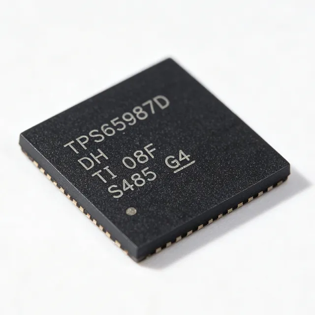
TPS65987DDHRSHR - USB Type-C PD Controller | Texas Instruments
The Texas Instruments TPS65987DDHRSHR is a stand-alone USB Type-C and Power Delivery (PD) controller with integrated power switches, designed for a single USB Type-C connector. It provides cable plug and orientation detection, communicates on the CC wire using the USB PD protocol, and enables the appropriate power path upon successful negotiation. The device supports USB 2.0, USB 3.0, and USB 3.1 data rates, and is housed in a 56-pin VQFN (RSH) package measuring 7x7 mm. It operates over a temperature range of -10°C to 75°C and is powered by a 3.3V supply. A USB Type-C PD controller is a specialized power management IC that manages power delivery and data communication over a USB Type-C connector. It handles cable detection, orientation, and power role negotiation (source, sink, or dual-role), enabling devices to negotiate voltage and current levels up to 100W. This controller sits between the USB connector and the system's power management unit, ensuring safe and efficient power transfer while supporting alternate modes like DisplayPort or Thunderbolt. Key features include integrated power switches for both source and sink paths, support for Dual-Role Power (DRP), Sink, and Source roles, and alternate mode configuration. The TPS65987D communicates using the USB PD protocol and includes a host interface for configuration and status monitoring. The device is designed for high-speed USB applications, with support for USB 3.1 data rates and integrated power path management. Technically, the TPS65987D integrates the CC logic, PD protocol engine, and power switches in a single package, reducing external component count and board space. It includes protection features such as overcurrent and overvoltage protection, and supports firmware updates via the host interface. The device is configurable through I2C or SPI, allowing flexible system integration. Typical applications include laptops, docking stations, monitors, power adapters, and other USB Type-C enabled devices that require PD negotiation and power switching. The integrated power switches simplify the design and reduce BOM cost, making it ideal for space-constrained applications. When designing with this device, ensure proper decoupling on the 3.3V supply and follow the recommended layout for the VQFN package to manage thermal performance. The device is currently in NRND (Not Recommended for New Designs) status, so consider the TPS65988 as a drop-in replacement for new designs.

TPS65988DDK - Dual-Port USB Type-C PD Controller | Texas Instruments
The Texas Instruments TPS65988DDK is a stand-alone dual-port USB Type-C and USB Power Delivery (PD) controller with integrated power switches, housed in a 56-pin VQFN (7x7 mm) package. It is certified by the USB-IF for PD3.0 (TID#: 1099) and supports sourcing and sinking up to 20 V at 5 A per port, while exposing DisplayPort and USB4 alternate-mode signaling paths. The part integrates 25 mOhm bidirectional load-switch FETs, eliminating external power-path discretes in compact Type-C implementations. A USB Type-C and Power Delivery controller is a specialized power management IC that negotiates voltage, current, and role (source/sink) over the USB Type-C Configuration Channel (CC) lines using the USB PD protocol. Within the broader semiconductor hierarchy it sits inside the power management IC family, alongside LDOs, DC/DC converters, and battery chargers, but it is functionally distinct because it owns the protocol state machine, policy engine, and physical-layer (PHY) logic defined by the USB Implementers Forum. Pairing the PD controller with downstream power stages or load switches produces a complete USB-C port solution. Key features of the TPS65988DDK include USB PD 3.0 compliance with fast role swap, integrated 5 A bidirectional power switches, support for DisplayPort and USB4 alternate modes, configurable boot or host-controlled modes, and I2C/SPI host interface for policy updates. Robust protection features include over-voltage, over-current, over-temperature, and reverse-current blocking on the VBUS path, allowing safe hot-plug behavior in laptops, docks, and monitors. Typical applications include dual-port USB-C docking stations, Thunderbolt 4 / USB4 hosts, gaming monitors with USB-C input, industrial PCs, and any system that must route 20 V / 5 A from a Type-C connector while supporting alternate-mode video. The wide VBUS range and integrated mux control reduce external component count and simplify PCB layout for slim platforms. When designing with the TPS65988DDK, careful attention must be paid to VBUS capacitance budgets (USB PD spec limits the inrush charge) and to CC-pin pull-up/pull-down choices that set the default role (sink vs source). Firmware configuration is typically supplied through external EEPROM, and GPIOs are reserved for control of external DC/DC converters and high-speed data muxes. This page synthesizes distributor pricing, same-family drop-in alternatives, and practical design notes not found in the manufacturer datasheet alone.

TPS66020YBGR - 20V Sink and 5V Source Switch | Texas Instruments
The Texas Instruments TPS66020YBGR is a full-featured USB-C power-path multiplexer with a 5 V source path, a 4 V to 22 V sink path, and a 3.3 V dead-battery LDO, housed in a 28-pin DSBGA (YBG) package measuring 1.61 mm by 2.81 mm. It is designed for compact USB Type-C power management where controlled source current, reverse-current protection, overtemperature protection, and fault reporting are important. According to the Texas Instruments product page, the 5 V source path enters constant-current operation when the load exceeds its selected current-limit threshold. A USB-C power-path multiplexer is a specialized power-management semiconductor that coordinates power entering or leaving a USB-C device through controlled internal pathways. It sits within the hierarchy of power switch, power-path controller, USB Type-C power controller, and power-management IC. Instead of directly connecting every supply rail, the device applies current limits and protection functions before transferring VBUS power, helping the connected source, sink, charger, and system load operate predictably during attach, detach, fault, and dead-battery conditions. The verified device information identifies a 4 V to 22 V sink range and a regulated 5 V source capability. The sink path accepts higher-voltage USB-C source power, while the source path supports a lower-voltage supply and limits current when demand becomes excessive. The integrated 3.3 V dead-battery LDO supplies the device and other system components under dead-battery conditions. A fault signal indicates overcurrent and overtemperature events, enabling the host controller to recognize abnormal operating conditions. Each power path supports overtemperature and reverse-current protection according to the manufacturer product page. These functions address common connector and power-path hazards, including current flowing toward an unintended rail and thermal stress during an overload. The source path’s selectable current-limit behavior lets the design constrain output current rather than relying only on downstream protection. Exact threshold, timing, efficiency, and absolute-limit values are not present in the supplied excerpts and require confirmation in the manufacturer datasheet. Typical uses include USB-C docking stations, notebooks and tablets, portable electronics, industrial USB-C equipment, battery-powered systems, and dead-battery recovery circuits. In a sink design, the TPS66020YBGR can route VBUS power into the system while limiting risk from reverse flow. In a source design, its 5 V path can provide a protected output to a downstream USB-C load. The 1.61 mm by 2.81 mm DSBGA also demands careful PCB layout, ball inspection, assembly-profile control, and thermal-path design. Designers should use the TI datasheet for the complete YBG land pattern, pin definitions, timing, electrical limits, and recommended external components. Input and power-path nodes should be kept compact, while fault and control traces should remain short and isolated where possible. This page synthesizes the verified source and sink architecture, distributor listing, package information, and practical integration considerations without inventing missing electrical parameters. Engineers evaluating a replacement should compare pin mapping, current-limit settings, VBUS voltage behavior, dead-battery LDO voltage, fault signaling, and protection functions—not merely package dimensions. Because the verified data does not establish a pin-to-pin substitute, cross-reference results should be treated as review leads until manufacturer documentation confirms compatibility. Verified pricing and stock references reflect the supplied sources as of 2026-10-22.
TPS66120YBGR - 22V USB-C Sink Power Switch | Texas Instruments
The Texas Instruments TPS66120YBGR is a USB-C Power Delivery high-voltage power switch for a sink with a 3.3 V dead-battery LDO, featuring an integrated 4 V to 22 V sink power path and a 28-pin DSBGA package measuring 1.61 mm by 2.81 mm. Its power path supports overtemperature and reverse-current protection, while VBUS overvoltage protection is configurable through an optional external resistor divider. These characteristics position it as a power-management IC for USB-C devices that must negotiate a power contract and safely distribute VBUS power during normal operation, fault handling, and dead-battery startup. A USB-C Power Delivery sink is the receiving side of a USB Type-C connection. The source supplies VBUS power, while the sink detects attachment, participates in power-role and power-contract negotiation, controls current flow, and protects its downstream system from unsafe voltage or current conditions. A sink power switch adds a controlled power path and protection functions; an LDO supplies a stable auxiliary rail. In the broader component hierarchy, the TPS66120 combines a USB-C interface, power switch, protection circuit, and low-dropout regulator within a single power-management device. The supplied manufacturer information identifies the TPS66120 series as a single-channel special-purpose switch IC with a 4 V to 22 V integrated sink path. It also documents a high-voltage VBUS LDO that can supply the device and other system components during dead-battery conditions. A fault signal indicates overtemperature events, enabling the host controller to detect a thermal shutdown rather than continuing to request unavailable power. The operating-temperature range shown on the official ordering page is -10 °C to 85 °C. The device is particularly relevant to compact USB-C power-acceptor designs where board area is constrained. Its 1.61 mm by 2.81 mm 28-ball DSBGA can reduce routing congestion around a USB-C connector and power-management circuitry, although fine-pitch assembly and inspection require capable PCB processes. The sink power path separates externally presented VBUS from downstream circuitry, while overtemperature and reverse-current protections address conditions that could otherwise stress system components. Typical uses include USB-C-connected battery chargers, portable instruments, industrial data loggers, battery-powered test equipment, and embedded systems that receive power through a USB-C port. The 3.3 V auxiliary LDO is useful when the downstream controller or external components need a stable rail even before the system’s main battery chemistry becomes operational. For automotive, medical, or extended industrial products, verify the full electrical limits, qualification status, and production lifecycle independently rather than inferring suitability from the commercial temperature grade alone. Designers should follow the manufacturer datasheet for VBUS capacitor selection, optional overvoltage-divider values, enable sequencing, fault handling, exposed-ball layout, and recommended PCB construction. In particular, preserve creepage and clearance around USB-C VBUS nodes and validate system behavior across source-capability advertisements, dead-battery startup, thermal stress, and unplug events. This page consolidates the verified ordering information, distributor observations, and cross-reference findings into an engineering-focused product record rather than adding unverified electrical or lifecycle claims.
TPS66121YBGR - 5V USB-C Sink Power Switch | Texas Instruments
The Texas Instruments TPS66121YBGR is a USB-C Power Delivery high-voltage power switch for a sink application, with a 4.5 V to 5.5 V operating input range and a 5 V dead-battery LDO in a 28-pin DSBGA package. It integrates USB-C sink power-path control, VBUS protection, and an LDO intended to supply the system during dead-battery conditions. The device is offered in the YBG package and is specified for a -10 °C to +85 °C temperature range. A USB-C power switch is a specialized power-management and interface component that controls current flow from a USB-C source toward a downstream system while protecting the sink path from unsafe voltage or fault conditions. The TPS66121 family combines USB-C Power Delivery-related sink functionality with a high-voltage VBUS LDO regulator, allowing a system to maintain operation when the external source is absent or below the normal operating range. Its 5 V output option is intended for devices that require a regulated auxiliary rail during dead-battery operation. The verified product information identifies the part as a one-channel switch IC with 28 DSBGA balls and a 4.5 V to 5.5 V power range. Distributor listings classify it as an analog switch, while Texas Instruments describes it as a USB-C Power Delivery high-voltage power switch for sinks with a 5 V dead-battery LDO. The -10 °C to +85 °C operating range makes it relevant to systems requiring controlled behavior across an extended industrial temperature span. Exact switch current, RON, fault thresholds, USB-C contract or PD behavior, and regulator accuracy were not included in the supplied verified data and therefore are not asserted here. Typical application contexts include USB-C-powered embedded systems, industrial controllers, battery-backed equipment, portable instruments, and consumer devices that must distinguish between an externally powered state and a dead-battery state. The integrated 5 V LDO can provide a controlled rail to the device and other system components during dead-battery conditions, according to the Texas Instruments product description. This integration may reduce the need for separate power-path switching and auxiliary supply circuitry, although the actual savings depend on the system architecture and protection requirements. Designers should begin with the USB-C connector and power-source requirements, then verify the device pinout, ball assignment, exposed-pad treatment, and recommended decoupling against the manufacturer datasheet. Because the supplied data does not include the complete electrical limits or pin map, those details must be checked before layout release. In particular, confirm VBUS voltage, current capability, enable or fault logic, thermal limits, and LDO behavior under load. This page combines the verified manufacturer description, distributor package data, operating-temperature information, and available sourcing references with explicit uncertainty markers for missing technical details. The result is intended to support early architecture and sourcing decisions while avoiding unsupported claims about electrical performance, safety compliance, or direct replacement parts.

TPS70928DBVR - 150mA, 30V, 2.8V Fixed LDO | Texas Instruments
The Texas Instruments TPS70928DBVR is a 150-mA, 30-V, ultra-low-IQ low-dropout (LDO) linear regulator with fixed 2.8V output, integrated enable, and reverse current protection, housed in a 5-pin SOT-23 (DBV) package. The device is designed for power-sensitive applications that require a stable post-regulation rail from a noisy upstream source. An LDO (Low-Dropout) linear regulator is a type of voltage regulator that maintains a stable output voltage even when the input-to-output voltage differential is very small. LDOs sit in the power management IC hierarchy below switching regulators and are chosen when low noise, small solution size, and fast transient response matter more than conversion efficiency. The TPS70928DBVR belongs to the TPS709 family, a low-IQ sub-category of LDO regulators. Key features include a fixed 2.8V output with 2% accuracy over temperature, a 30V maximum input rating, 1 uA typical quiescent current, 1.7 uA ground-pin current, reverse current blocking to prevent output-to-input backfeed, and an active-low enable pin for power sequencing. The 150-mA continuous output rating supports low-power microcontroller, sensor, and always-on rails. The TPS70928DBVR uses a precision band-gap reference and an error amplifier architecture that delivers tight load and line regulation. Reverse-current protection is implemented with a back-to-back FET topology so the device tolerates scenarios where the output rail is held up by another supply. The SOT-23-5 footprint plus minimal external components (1 uF ceramic input/output) supports ultra-compact layouts. Typical applications include always-on microcontroller rails in battery-powered IoT devices, sensor and metering subsystems, industrial point-of-load regulation from 24V/12V buses, and portable medical or wearable electronics where 1 uA quiescent current is critical. The wide 30V input range simplifies designs sharing a common input bus. When designing with this device, observe the minimum input-to-output headroom required for regulation and place the 1 uF ceramic input and output capacitors as close to the pins as possible. The enable pin allows the host MCU to disable the rail during deep sleep, extending battery life. This page synthesizes distributor pricing, drop-in alternatives from the TPS709 family and competitors, and practical design notes that supplement the manufacturer datasheet.
TPS70933QDBVRQ1 - 150mA, 30V Automotive LDO | Texas Instruments
The Texas Instruments TPS70933QDBVRQ1 is an automotive-qualified, 150-mA, 30-V ultra-low-IQ low-dropout (LDO) linear regulator with reverse current protection, delivering a fixed 3.3V output in a 5-pin SOT-23 (DBV) package. Key parameters include a 150 mA maximum output current, 30 V maximum input voltage, 1 uA typical quiescent current, and 3.3V fixed output. The device is specified over the -40C to +125C automotive temperature range and carries the AEC-Q100 automotive qualification. An LDO (Low-Dropout) linear regulator is a type of voltage regulator that maintains a stable output voltage even when the input voltage is very close to the output voltage. LDOs sit within the broader taxonomy of linear regulators, which in turn belong to the voltage regulator and power management IC category. Unlike switching regulators, LDOs dissipate the difference between input and output as heat, but they introduce no switching noise - making them ideal for noise-sensitive analog and RF signal chains. Key features of the TPS70933QDBVRQ1 include an integrated enable pin for power sequencing, internal current limit, thermal shutdown, and reverse current protection that prevents current flow from output back to input when the input rail collapses. The 1 uA quiescent current extends battery life in always-on applications, while the wide 30 V input range accommodates load-dump transients common in 12V automotive buses. The device uses a PNP pass element architecture with internal compensation, requiring only 1 uF ceramic output capacitance for stability. Reverse current protection eliminates the need for external blocking diodes in power-muxing circuits, reducing BOM count and board area in space-constrained modules. Typical applications include automotive body electronics, always-on battery-powered sensors, infotainment standby rails, and industrial IoT edge nodes. The TPS70933QDBVRQ1's combination of ultra-low IQ, reverse current blocking, and AEC-Q100 qualification makes it particularly suitable for designs that must survive cold-crank and load-dump events while drawing minimal quiescent current from the vehicle battery. When designing with this part, ensure the input capacitor meets the manufacturer's minimum ESR requirements and place it within 5 mm of the IN pin to handle high di/dt transients. The reverse current protection block is rated to prevent back-feeding when VOUT exceeds VIN, which is critical during power-down sequencing in multi-rail automotive systems. This page synthesizes distributor pricing, drop-in alternatives, and practical design notes not found in the standalone TPS70933QDBVRQ1 datasheet.
TPS70950DBVR - 150mA, 30V Ultra-Low IQ LDO Regulator | Texas Instruments
The Texas Instruments TPS70950DBVR is a 150-mA, 30-V, ultra-low quiescent current (1 uA typical) low-dropout (LDO) linear regulator with a fixed 5.0V output, housed in a 5-pin SOT-23 (DBV) package. The device accepts input voltages from 2.7V to 30V, supports 2% output accuracy over temperature via a precision band-gap reference, and includes an active-low enable pin for power sequencing. Reverse-current blocking protects the system when VIN drops below VOUT. An LDO (Low-Dropout) linear regulator is a type of voltage regulator that maintains a stable output voltage even when the input voltage is only slightly above the output. LDOs sit within the broader hierarchy of linear regulators -> voltage regulators -> power management ICs -> semiconductors. Unlike switching regulators, LDOs do not introduce EMI but dissipate the difference (VIN - VOUT) * IOUT as heat. They are preferred where low noise, simplicity, and fast transient response are critical. The TPS70950DBVR delivers 150 mA continuous output current, has a typical dropout of 690 mV at full load, and offers integrated thermal shutdown plus current-limit protection. The SOT-23-5 footprint (2.9 mm x 1.6 mm) makes it one of the smallest wide-input LDOs available, ideal for space-constrained industrial and battery-powered designs. Architecturally, the part uses a PMOS pass element, which lowers ground-pin current to a minimum and enables true reverse-current blocking without a secondary diode. The 1 uA IQ makes the TPS70950DBVR well-suited to always-on, standby, or sleep-mode rails in IoT, metering, and remote-sensor applications. Typical applications include battery-powered IoT sensors, PLC analog I/O modules, portable medical monitors, smart meters, and post-regulation of switching converters where a clean 5V rail is required. The wide input range also allows direct connection to 12V/24V industrial bus rails. When designing with this device, place a 1 uF or larger ceramic input capacitor close to IN, and a 1 uF or larger low-ESR ceramic output capacitor close to OUT. Account for dropout at the worst-case 150 mA load and the lowest VIN in your system; for a 5V output from a battery below 5.69V the regulator will drop out of regulation. This page synthesizes distributor pricing, drop-in alternatives, and practical design notes not found in the manufacturer datasheet. Engineers searching for a wide-VIN, ultra-low-IQ 5V LDO in SOT-23-5 will find the TPS70950DBVR datasheet, parameters, and verified alternatives below.

TPS7133QDR - 3.3V 500mA LDO with RESET | Texas Instruments
The Texas Instruments TPS7133QDR is a micropower, low-dropout (LDO) PMOS linear voltage regulator delivering a fixed 3.3V output at up to 500mA in an 8-pin SOIC (D) package. It integrates an enable pin and a power-on RESET output with programmable delay, providing supervisor functionality on the same silicon as the regulator. An LDO regulator is a type of linear voltage regulator that maintains a stable output even when the input-output differential is very small. Unlike switching regulators, LDOs produce no switching noise, making them part of the broader power management IC (PMIC) family used to post-regulate noisy DC-DC rails and supply analog loads. Key features include a very low dropout voltage of 47mV at 100mA load, low quiescent current of 285uA, 274uVrms output noise, and 54dB PSRR at 120Hz. The PMOS pass element replaces the conventional pnp transistor, achieving an order-of-magnitude reduction in dropout voltage and quiescent current over older LDO architectures. Protection features include over-current and over-temperature shutdown, and the device operates from -40C to +125C junction temperature with a maximum input of 10V. The RESET output asserts low when the output falls out of regulation and includes a delay to allow processor power rails to stabilize, eliminating a separate supervisor IC in microcontroller systems. Typical applications include battery-powered portable instruments, 3.3V microcontroller and DSP power supplies, and post-regulation of switching converter outputs where low noise and fast transient response matter. Design tip: use a 0.1uF input bypass and at least a 10uF output capacitor with low ESR for stability, and keep the enable pin driven or tied high to avoid floating-pin leakage in always-on designs.

TPS715-Q1 - 50mA, 24V, 3.2uA IQ LDO | Texas Instruments
The Texas Instruments TPS715-Q1 is an automotive-grade, low-dropout linear regulator (LDO) delivering up to 50 mA of output current with an ultra-low quiescent current of only 3.2 uA (typical) across the entire load range. It accepts a wide input voltage range up to 24 V and is available in fixed and adjustable output versions in a miniaturized 2.00 mm x 1.25 mm, 5-pin SC-70 (DCK) package. An LDO (low-dropout regulator) is a type of linear voltage regulator that maintains a stable output voltage even when the input voltage is only slightly above the output. Within the power-management IC hierarchy, the TPS715-Q1 sits at the point-of-load regulation stage, converting higher-voltage battery or automotive rails into clean, low-noise supplies for microcontrollers, sensors, and analog circuitry. Key features include the 3.2 uA quiescent current that dramatically extends battery life in always-on systems, a wide input range supporting 24 V industrial and 12 V automotive rails, an internal soft-start that limits inrush current during startup, and a built-in overcurrent limit that protects the device during load shorts or fault conditions. The low dropout voltage allows efficient operation from already-regulated or heavily loaded supplies. Architecturally, the TPS715-Q1 uses a precision bandgap reference and an error amplifier driving a PMOS pass element, with the internal soft-start ramping the output to avoid excessive inrush when powering capacitive loads. Its micropower bias design keeps ground current essentially flat from no-load to full 50 mA load, simplifying power budget calculations for sleep and standby modes. Typical applications include battery-powered portable instrumentation, always-on wake-up and keep-alive supplies for automotive modules, and power-management attachments to low-power microcontrollers such as the MSP430 and C2000 families, where every microamp of quiescent current affects system lifetime. Design consideration: at only 50 mA maximum output, size the external output capacitor per datasheet stability requirements and account for thermal headroom at 24 V input, where dissipation at full load approaches 1 W - verify junction temperature in the tiny SC-70 footprint.

TPS71501DCKR - 50mA, 24V Wide-Input LDO Regulator | Texas Instruments
The Texas Instruments TPS71501DCKR is a 50 mA, wide-input, low-dropout (LDO) linear regulator housed in a 5-pin SC-70 (DCK) package. It accepts input voltages from 2.5 V to 24 V, supports an adjustable output from 1.2 V to 15 V via an external resistor divider, and consumes only 3.2 uA of quiescent current. A 415 mV typical dropout at full 50 mA load extends usable operation near the lower rail, and stability is guaranteed with any output capacitor greater than or equal to 0.47 uF. What is an LDO (Low-Dropout) linear regulator? An LDO is a type of voltage regulator that maintains a stable output voltage even when the input voltage is only marginally above the desired output. Within the broader taxonomy, an LDO is a linear regulator, which is a subclass of voltage regulators, sitting under power management ICs in the semiconductor hierarchy. Wide-input LDOs such as the TPS71501 differ from standard LDOs by tolerating much higher VIN, making them suited for industrial 24 V rails, battery stacks up to ~20 V, and post-bridge-rectifier supplies. Key features of the TPS71501DCKR include 3.2 uA quiescent current for battery-friendly standby, 415 mV typical dropout at 50 mA, internal current limit, and thermal shutdown protection. The SC-70-5 footprint occupies roughly 2.0 mm x 1.25 mm of board area, enabling dense designs in portable equipment. The device does not require an enable pin in the basic TPS71501 family, simplifying MCU-attached power trees. The TPS71501 uses a PMOS-pass architecture with a precision bandgap reference. The combination of low IQ and wide VIN lets it sit directly on a high-voltage battery or bus while still drawing negligible standby current, and the absence of a minimum-load requirement (true no-load stability) avoids the dummy-resistor tricks needed by some competing parts. Typical applications include always-on microcontroller rails in battery-powered IoT nodes, industrial 24 V sensor conditioning, post-bridge auxiliary supplies, and low-current analog references. The wide input range is especially valuable where the upstream source is a rectified mains-isolated rail. When designing with the TPS71501, place input and output capacitors close to the IC, keep the FB resistor divider traces short, and verify worst-case dropout at minimum VIN and maximum load. For higher-current rails (>200 mA), select a different TI LDO. This page combines manufacturer specifications, distributor stock and pricing, drop-in alternatives in the same SC-70-5 footprint, and practical design notes not consolidated in the TPS715 datasheet.
TPS71825-12DRVT - 200mA Dual-Output Low-Noise LDO | Texas Instruments
The Texas Instruments TPS71825-12DRVT is a dual-channel, low-dropout (LDO) linear regulator that delivers two independent fixed outputs of 2.5 V and 1.2 V at up to 200 mA each, packaged in a 2 mm x 2 mm 6-pin WSON (DRV) package. It accepts a wide 2.7 V to 6.5 V input voltage range and achieves a low 230 mV dropout at full 200 mA load on each rail. The regulator is engineered for battery-powered and noise-sensitive applications requiring two clean supplies from a single small footprint. What is an LDO (Low-Dropout) linear regulator? An LDO is a type of linear voltage regulator that maintains a stable, low-noise output voltage even when the input voltage is only marginally higher than the output. LDO regulators sit within a system hierarchy: they are a sub-category of linear regulators, which in turn belong to voltage regulators, the foundation of power management ICs in any electronic system. Unlike switching converters, LDOs do not introduce switching ripple, making them ideal for analog, RF, and audio power rails. Key features of the TPS71825-12DRVT include high power-supply rejection ratio (PSRR), low output noise, fast start-up, and an active-high enable pin for individual rail sequencing or shutdown. The integrated discharge and soft-start functions limit inrush current at power-on. The TPS718xx family's small WSON-6 footprint combined with dual outputs makes it especially attractive for space-constrained portable designs that need two low-noise rails simultaneously. Architecturally, the device uses a PMOS pass-element topology per rail, which contributes to its low dropout and low quiescent current behavior. The high PSRR reduces residual ripple from upstream DC-DC converters, while the low output noise floor preserves signal integrity in analog and RF signal chains that share the same battery or bus. Typical applications include smartphone RF transceiver power, portable media players, wireless sensor nodes, camera modules requiring dual-rail analog and digital supplies, handheld medical monitors, and any battery-powered system requiring two low-noise rails from a single chip. When designing with this part, place input and output capacitors as close to the IC as possible, use low-ESR ceramic capacitors on each output, and respect the 230 mV dropout headroom at maximum load to maintain full regulation. This page synthesizes distributor pricing, dual-rail drop-in alternatives, and practical design notes not found in the manufacturer datasheet alone.

TPS73501DRBR - 500mA Low-IQ High-PSRR LDO | Texas Instruments
The Texas Instruments TPS73501DRBR is a 500-mA low-dropout (LDO) linear regulator with an enable pin, offering ultra-low quiescent current and high PSRR. It operates from an input voltage range of 2.7 V to 6.5 V and provides an adjustable output from 1.25 V to 6 V. The device is available in an 8-pin VSON (DRB) package (3x3 mm) and is designed for battery-powered and noise-sensitive applications. An LDO (Low-Dropout) linear regulator is a type of voltage regulator that maintains a stable output voltage even when the input voltage is very close to the output voltage. It is a subclass of linear regulators that use a pass transistor operating in its linear region to drop excess voltage. LDOs are essential power management ICs providing clean, low-noise supply rails to sensitive analog and digital circuits within a broader power management architecture. Key features include a low quiescent current of 45 uA (typical), high PSRR of 68 dB at 1 kHz, and low output noise. The enable pin allows power sequencing and shutdown to reduce power consumption. Overcurrent and thermal shutdown protection ensure robust operation in demanding environments. The TPS73501DRBR uses a CMOS process technology, contributing to low quiescent current and high efficiency at light loads. The adjustable output is set with an external resistor divider, providing design flexibility. The VSON package with an exposed thermal pad enhances heat dissipation, allowing the regulator to deliver up to 500 mA with proper PCB layout. Fast start-up and excellent line and load transient response round out the AC performance. Typical applications include powering microcontrollers, sensors, and RF transceivers in battery-operated devices, as well as providing clean supply rails for audio and precision analog circuits. The low dropout voltage of 0.5 V at 500 mA ensures efficient operation even with small input-to-output voltage differences. When designing with this device, ensure adequate input and output capacitance (typically 1 uF) placed close to the pins. The enable pin can be tied to VIN if not used. For optimal noise performance, a noise bypass capacitor can be added to the NR pin.
TPS73501QDRBRQ1 - 500mA Low-Noise LDO, AEC-Q100 | TI
The Texas Instruments TPS73501QDRBRQ1 is an automotive-qualified (AEC-Q100) 500-mA low-dropout linear regulator featuring low quiescent current, low output noise, and high PSRR. It provides an adjustable output voltage from 1.25V to 6V and operates from -40C to +125C in an 8-pin VSON (DRB) 3x3 mm package with an enable pin for power sequencing. An LDO (low-dropout regulator) is a type of linear voltage regulator that maintains a regulated output even when the input voltage is only slightly above the output. Within the power management IC hierarchy, LDOs sit downstream of switching converters to provide clean, low-noise rails for noise-sensitive loads. Unlike DC-DC buck converters, an LDO adds no switching ripple, trading efficiency for output purity. Key features of the TPS735-Q1 family include 500-mA output current capability, very low dropout voltage for high-efficiency operation, low quiescent current that extends battery and standby life, and high PSRR that suppresses upstream switching-converter ripple. The enable pin (active functionality confirmed by TI product page) supports rail sequencing in multi-supply systems. The VSON-8 (DRB) package with exposed pad provides good thermal performance for a compact footprint. The device uses a low-noise architecture with a precision reference; for lowest output noise, an optional noise-bypass/noise-reduction capacitor at the NR pin reduces reference noise bandwidth (refer to TI datasheet). Internal protection includes current limit and thermal shutdown. Typical applications include automotive ADAS camera and radar module power rails, infotainment audio/RF supplies, cluster displays, and post-regulation of 3.3V or 5V switching rails in industrial systems requiring low-noise analog rails. Design tip: with a 5V input and 3.3V output at 500 mA, the device dissipates about 0.85W; verify junction temperature using the DRB package theta_JA with adequate PCB copper on the exposed thermal pad, per TI layout guidelines.
TPS73633DBVR - 3.3V 400mA LDO Regulator | SOT-23-5 | Texas Instruments
The Texas Instruments TPS73633DBVR is a 400 mA high-accuracy ultra-low-dropout (LDO) linear regulator with a fixed 3.3 V output, reverse current protection, and an active-high enable input, housed in a 5-pin SOT-23 (DBV) package. Per the TI part details page, it accepts an input voltage range of 1.7 V to 5.5 V and operates across -40 °C to +125 °C. The architecture is built on an advanced BiCMOS process and uses an NMOS pass element in a voltage-follower topology that delivers a typical dropout of just 75 mV at 400 mA. An LDO (Low-Dropout) linear regulator is a type of voltage regulator that maintains a constant output voltage even when the input voltage approaches the output voltage. Positioned in the broader hierarchy, an LDO is a sub-class of linear regulator, which sits within the voltage regulator family, itself part of the power management integrated circuit (PMIC) category in mixed-signal semiconductors. LDOs are favored over switching regulators when the design demands ultra-low noise, fast transient response, and a minimal external component count. Key features of the TPS73633DBVR include: stability with NO output capacitor or with any capacitor type/value (cap-free operation), 75 mV typical dropout at 400 mA, ±0.5 % overall output accuracy, near-constant ground pin current over load, and integrated reverse-current protection that blocks discharge from the output back into the input when the input falls. The small SOT-23-5 footprint and 5 µA quiescent current make it attractive for portable, battery-powered designs. The TPS736 family uses an NMOS pass transistor driven by a high-drive charge pump and a precision bandgap reference. This topology yields low dropout and high reverse blockage while keeping the GND current nearly flat across the load curve, preserving efficiency at light loads where battery life matters most. The part includes internal current limiting and thermal shutdown for fault protection. Typical applications include portable/battery-powered equipment (handheld terminals, wearables, IoT sensor nodes), point-of-load regulation for microcontrollers and wireless modules, post-regulation following a DC-DC switcher to clean ripple, and industrial sensors running off 3.3 V rails. When designing with this part, the user can simply tie IN to OUT through a short trace if no bypass cap is available - the regulator is stable either way. Add a 0.1 µF X7R input cap if the source impedance is high or the input trace is long. This page synthesizes TI datasheet parameters, distributor pricing, drop-in SOT-23-5 alternatives, and practical design notes that you will not find in the bare datasheet PDF - including cross-brand pin-compatible equivalents and parametric trade-offs across the TPS736 family.

TPS73801DCQR - 1A, 20V Low-Noise LDO | Texas Instruments
The Texas Instruments TPS73801DCQR is a low-dropout (LDO) linear regulator optimized for fast transient response, supplying 1.0A of output current with a dropout voltage of only 300mV. It operates from an input voltage range of 2.7V to 20V and provides an adjustable output voltage from 1.21V to 20V, set by external resistors. The device is housed in a 6-pin SOT-223 (DCQ) package with a thermal tab for enhanced heat dissipation, making it suitable for compact, power-dense designs. An LDO (Low-Dropout) linear regulator is a type of voltage regulator that maintains a stable output voltage even when the input voltage is very close to the output voltage. Unlike standard linear regulators, LDOs use a pass transistor with a low saturation voltage, allowing operation with minimal headroom. In the power management hierarchy, an LDO is a linear regulator, which is a voltage regulator, which falls under power management ICs used in virtually all electronic systems. Key features include low output noise of 45 uVRMS (up to 100 kHz), a quiescent current of 1mA (dropping below 1uA in shutdown), and controlled quiescent current in dropout, which prevents unexpected current spikes. The device also provides reverse current and reverse voltage protection, eliminating external protection diodes. Its fast transient response minimizes output deviation during load steps, making it ideal for powering microprocessors, DSPs, and other digital loads. Technically, the TPS73801 uses a PMOS pass element with a precision bandgap reference, achieving excellent line and load regulation. The adjustable output is set via an external resistor divider, and a shutdown (EN) pin supports power sequencing. The device is fully specified over the -40C to +125C junction temperature range. Typical applications include point-of-load regulation for FPGAs, ASICs, and microcontrollers, plus noise-sensitive analog supplies for audio and RF circuits, precision ADC/DAC references, and PLL/VCO rails. The wide input range also supports industrial 24V bus systems with adequate headroom. When designing with the TPS73801, ensure adequate input-to-output headroom to maintain regulation at all loads, and place input and output capacitors close to the device to minimize parasitic inductance and ensure stability.

TPS73801QDCQRQ1 - 1A Low-Noise LDO, AEC-Q100 | TI
The Texas Instruments TPS73801QDCQRQ1 is an automotive-grade, low-dropout (LDO) linear regulator delivering up to 1.0A of output current with a dropout voltage of only 300mV at full load. Housed in a 6-pin SOT-223 (DCQ) package, it accepts input voltages up to 20V and provides an adjustable output, making it well suited for post-regulation of switching converter rails in automotive and industrial systems. The Q1 suffix denotes AEC-Q100 qualification for automotive applications. An LDO regulator is a type of linear voltage regulator within the broader power management IC hierarchy that maintains a stable output voltage even when the input voltage is only slightly higher than the output. Unlike switching regulators, LDOs add no switching noise and excel at cleaning up noisy DC rails. The TPS73801 belongs to TI's low-noise, fast-transient-response LDO family. Key features include fast transient response optimized for load steps, an operating quiescent current of 1mA that drops to less than 1uA in shutdown, and quiescent current that is well controlled and does not rise in dropout - a common problem with other regulators. The device also integrates reverse current and reverse voltage protection, protecting the output stage when input collapses below output, an important reliability feature in automotive cold-crank and load-dump scenarios. Architecturally, the TPS73801 uses a precision reference and error amplifier topology tuned for transient performance, allowing tight regulation during fast microcontroller load transitions without large output capacitor banks. Typical applications include automotive body electronics and ADAS power rails, post-regulation of DC-DC converter outputs powering microcontrollers and sensors, and industrial point-of-load supplies where low noise and fast response are required. Design tip: ensure adequate input-to-output headroom for the 300mV dropout at 1A, and use the shutdown pin (quiescent current under 1uA) to save power in sleep states. Prices referenced as of 2026-08-29.
TPS74501PQWDRVRQ1 - Automotive 500mA LDO w/ Power-Good | TI
The Texas Instruments TPS74501PQWDRVRQ1 is an AEC-Q100 Grade 1 qualified, 500 mA ultra-low-dropout (LDO) linear regulator with integrated power-good (PG) functionality, packaged in a 6-pin 2 mm x 2 mm wettable-flank WSON (DRV) package. The device supports an input voltage range from 1.5 V to 6.0 V and provides an adjustable output from 0.55 V to 5.5 V, with the TPS74501 variant specifically being the adjustable-output version of the TPS745-Q1 family. An LDO (Low-Dropout) linear regulator is a type of voltage regulator that maintains a stable output voltage even when the input voltage approaches the output voltage, characterized by very low dropout voltage and high power supply rejection ratio (PSRR). Within the broader power management hierarchy, the TPS74501PQWDRVRQ1 sits as a linear regulator, a sub-category of voltage regulators, which in turn are part of the power management IC (PMIC) family used to deliver clean, low-noise rails to digital and analog loads. Key features include very low quiescent current (I_Q) for always-on systems, high PSRR across frequency for rejecting upstream switching-converter ripple, fast line and load transient response, and an open-drain power-good output for rail monitoring and processor reset coordination. The wettable-flank WSON package with optical-inspection-ready terminations supports automated optical inspection (AOI) on automotive PCB assembly lines. Internal protection features include thermal shutdown and current limit. Operating junction temperature spans -40 C to +150 C, qualifying the part for AEC-Q100 Grade 1 automotive stress profiles. The TPS74501PQWDRVRQ1 uses a low-resistance P-channel pass element topology that delivers the low-dropout performance while maintaining an architecture that contributes to its low I_Q. The high PSRR makes the regulator well suited as a post-regulator following a switching DC-DC converter, cleaning the residual switching ripple before it reaches noise-sensitive analog blocks. The wettable flanks of the WSON-6 package enable solder-joint inspection on automotive production lines. Typical applications include automotive ADAS sensor power rails, rear-view and surround-view camera modules, infotainment processors and telematics modules, body electronics and lighting controllers, and industrial PLC I/O supply rails. Anywhere a 0.55 V to 5.5 V clean low-noise rail at up to 500 mA is required in a small footprint, the TPS74501PQWDRVRQ1 is a strong fit. When designing with this device, place the input and output ceramic capacitors as close as possible to the IC pins to maximize PSRR and load-transient performance. Always verify the power-good pull-up voltage does not exceed the absolute maximum rating, and respect the junction-to-ambient thermal resistance to avoid thermal shutdown in continuous high-power conditions. This page synthesizes distributor stock data, drop-in same-package alternatives, and practical design notes not assembled in the manufacturer datasheet.

TPS74601PBDRVR - 1A Adjustable LDO with Power Good | Texas Instruments
The Texas Instruments TPS74601PBDRVR is a 1-A ultra-low-dropout (LDO) linear regulator with adjustable output from 0.55V to 5.5V, housed in a 6-pin WSON (DRV, 2x2 mm) package with an exposed thermal pad. The device features an ultra-low 225 mV dropout at full 1-A load, an integrated power-good indicator, an active-high enable input, and only 25 uA typical quiescent current, making it suited for power-sensitive designs. According to TI datasheet literature, input voltage ranges from 1.5 V to 6.0 V with an absolute maximum of 6.5 V, and output accuracy is rated at 1% over the -40C to +125C operating range. An LDO (Low-Dropout) linear regulator is a class of voltage regulator that maintains a tightly regulated output voltage even when the input-to-output differential (dropout) is very small - typically a few hundred millivolts. In the broader system taxonomy, an LDO sits below the category of linear regulators, which in turn sits below voltage regulators, and ultimately below power management ICs. LDOs convert a higher DC rail to a lower, accurate DC rail without the switching noise of a buck converter, trading efficiency for clean output, which is essential when the load is sensitive to ripple or high-frequency noise. Key features that distinguish the TPS74601 include a 45 dB PSRR at 100 kHz, internal soft-start, foldback overcurrent protection, output discharge, and an open-drain PG output that asserts when the output is within regulation. The TPS74601PBDRVR uses a PNP bipolar pass element architecture, which provides the low dropout characteristic and high efficiency at moderate VIN/VOUT differentials. Stability is achieved with only a 1 uF ceramic output capacitor, simplifying BOM and lowering solution cost. Typical applications include point-of-load regulation for microcontrollers, FPGAs, SoCs and DDR memory in portable and battery-powered equipment, USB-powered peripherals, building automation, and industrial sensor nodes. The small 2x2 mm footprint and high accuracy suit dense board layouts where board area is constrained. When designing with the TPS74601PBDRVR, ensure VIN-VOUT headroom stays above 225 mV at full load, place the 1 uF input and output ceramic capacitors as close to the IC as possible, and use the PG output for rail sequencing with downstream loads.
TPS74601PQWDRVRQ1 - 1A Automotive LDO w/ PG | WSON-6 | Texas Instruments
The Texas Instruments TPS74601PQWDRVRQ1 is an automotive-qualified, 1-A, ultra-low-dropout (LDO) linear regulator with integrated power-good (PG) output, housed in a compact 6-pin WSON package (2 mm x 2 mm) with wettable flanks for optical inspection. It accepts input voltages from 1.5 V to 6.0 V and provides an adjustable output from 0.55 V to 5.5 V, with 25 uA typical quiescent current and 53 uVrms output noise (per JLCPCB parameter listing). An LDO (Low-Dropout) linear regulator is a type of voltage regulator that maintains a stable output voltage even when the input voltage is very close to the output voltage. It belongs to the broader power-management-IC hierarchy: LDO -> linear regulator -> voltage regulator -> power management IC -> semiconductor. Unlike a switching regulator, an LDO does not introduce switching noise, making it ideal for post-regulation after a noisy DC-DC converter or for direct battery-powered rails. Key features of the TPS74601PQWDRVRQ1 include 38 dB PSRR at 100 kHz, 895 mV maximum dropout at 1 A load, integrated UVLO, over-current protection, over-temperature protection, and short-circuit protection. The wettable-flank 6-WSON package (2x2 mm) is significantly smaller than competing 8-pin alternatives and supports automated optical inspection (AOI) for automotive PCB assembly lines. Architecturally, the TPS746-Q1 uses a P-channel MOSFET pass element that eliminates the need for a bias supply and minimizes ground current variation across load. The integrated open-drain PG pin flags output-voltage readiness for downstream MCUs and FPGAs, simplifying multi-rail sequencing in zonal automotive E/E architectures. Typical applications include automotive camera modules, ADAS sensor power, body-control modules, infotainment processors, and post-regulation for switching converters. The -Q1 suffix indicates AEC-Q100 qualification for Grade 1 automotive environments (-40C to +125C junction). When designing with this device, place input/output ceramics as close to the pins as possible and observe the 1.7 A typical current limit when calculating transient load response. The PG pull-up resistor should be tied to a known-good rail and never left floating. This page synthesizes distributor pricing, AEC-Q100-qualified drop-in alternatives, and practical design notes not aggregated on a single manufacturer page.