5CGXBC7C7F23C8N vs XC7A100T-2FGG484I Comparison
Detailed side-by-side comparison of 5CGXBC7C7F23C8N by Intel and XC7A100T-2FGG484I by AMD. Compare key specifications, electrical parameters, packaging, lifecycle status, pricing, and availability to determine the best component for your design requirements.

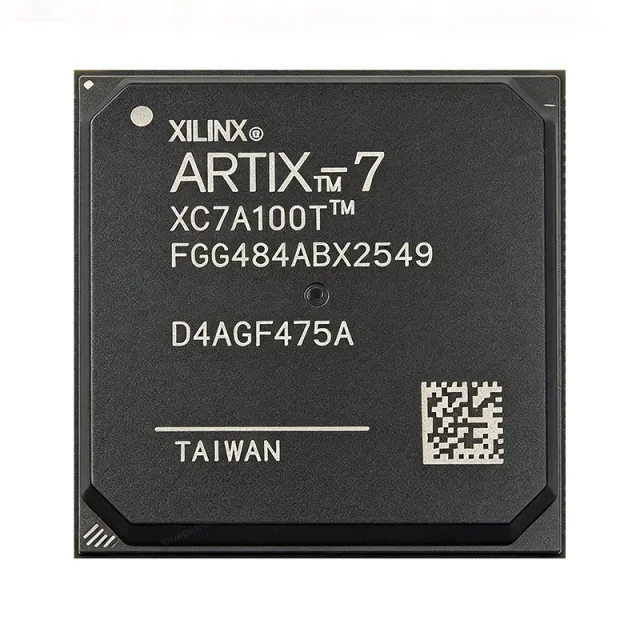
Specification Comparison
| Parameter | 5CGXBC7C7F23C8N | XC7A100T-2FGG484I |
|---|---|---|
| Brand | Intel | AMD |
| Category | FPGA & CPLD | FPGA & CPLD |
| Lifecycle Status | Active | Active |
| Stock Status | In Stock | In Stock |
| Unit Price (USD) | $29.70 | $45.94 |
| Series | Cyclone V GX | — |
| Family | 5CGXC7 (logic density tier) | — |
| Logic Elements (LE) | 149,500 | — |
| Embedded Memory Bits | 7,880,704 bits (~963 Kbytes) | — |
| Embedded 18x18 Multipliers | 312 | — |
| Transceivers | 6 channels, up to 3.125 Gbps | — |
| User I/O Pins | 240 | — |
| Core Voltage | 1.1 V | — |
| Process Technology | TSMC 28 nm low-power | 28 nm |
| Package | 484-ball FBGA (F23) | 484-ball FBGA (FGG484) |
| Mounting Type | Surface Mount (BGA) | Surface Mount |
| Temperature Grade | Commercial (0C to 85C) | — |
| Speed Grade | 8 (slowest commercial) | -2 |
| Hard Memory Controllers | 2 | — |
| PLLs | Up to 8 | — |
| Global Clock Networks | Up to 16 | — |
| RoHS Status | Compliant | — |
| Logic Cells | — | 101440 |
| User I/O | — | 285 |
| Block RAM | — | 4976640 bits |
| DSP Slices | — | 240 (DSP48E1) |
| Clock Management Tiles | — | 10 (MMCM + PLL) |
| Maximum Fabric Frequency | — | 628 MHz |
| Core Supply Voltage | — | 0.95 V to 1.05 V (nominal 1.0 V) |
| Package Dimensions | — | 23 mm x 23 mm |
| Operating Temperature | — | -40C to +100C (Industrial) |
| Memory Interface | — | DDR3 up to 1066 Mb/s |
| Soft Processor Support | — | MicroBlaze |
| Analog Mixed Signal | — | XADC 12-bit ADC (on-chip voltage and temperature monitoring) |