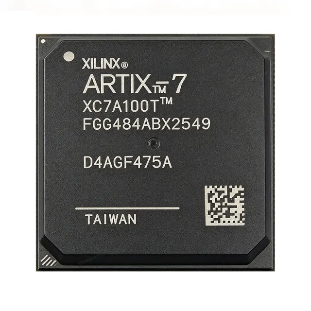
XC7A100T-2FGG484I - Artix-7 FPGA, 285 I/O, 484-FBGA | AMD
MPN: XC7A100T-2FGG484I ✓ Active| Qty | Unit Price | Extended |
|---|---|---|
| 1 | $78.75 | $78.75 |
| 10 | $56.875 | $568.75 |
| 100 | $50.3125 | $5,031.25 |
| 500 | $48.125 | $24,062.50 |
| 1,000 | $45.9375 | $45,937.50 |
XC7A100T-2FGG484I Overview
An FPGA is a reconfigurable integrated circuit whose logic fabric, interconnect, and I/O cells can be programmed after manufacturing, unlike fixed-function ASICs. Within the hierarchy of programmable logic, the Artix-7 family sits between the smaller Spartan-7 and the larger Kintex-7 in AMD's (formerly Xilinx) 7-series, balancing logic density, DSP throughput, and transceiver performance for cost-optimized mid-range designs.
Key differentiating features include 240 DSP48E1 slices for parallel signal processing, 10 clock management tiles (CMTs) combining MMCM and PLL blocks, and support for MicroBlaze soft processor cores and DDR3 memory interfaces up to 1,066 Mb/s. The -2 speed grade fabric can run at up to 628 MHz, and the device integrates Analog Mixed Signal (AMS) blocks including a 12-bit ADC for on-chip voltage and temperature monitoring.
Architecturally, the 28nm high-performance/low-power process enables high logic utilization with low static power. The core supply operates from 0.95V to 1.05V nominal 1.0V, with separate VCCAUX and bank-selectable VCCO rails supporting multiple I/O voltage standards. Partial reconfiguration allows flexible in-system updates without full device reprogramming.
Typical applications include motor control, industrial networking and automation, medical imaging front ends, and software-defined radio, where the 285 I/O count and DSP density are well matched. The 484-ball FGG484 package offers a balanced footprint of approximately 23mm x 23mm for moderate-to-high I/O designs.
A key design consideration is power: multiple rails (VCCINT, VCCAUX, VCCO) require specific power sequencing, ramp rates, and decoupling networks. Use the AMD Vivado Design Suite for implementation and the UG475 package pinout files for PCB footprint verification.
This page synthesizes distributor pricing, drop-in alternatives, and practical design notes not found in the manufacturer datasheet, as of 2026-09-11.
Drop-in alternatives for XC7A100T-2FGG484I — same package, pin-to-pin compatible. Different-package parts requiring PCB rework are excluded.
Variants in this series
Same-series models that are drop-in compatible with XC7A100T-2FGG484I (same form factor and footprint) — differing in Package, Operating Temperature, Process Technology, Block RAM, Logic Cells.
Quick Comparison Tool — Select alternative parts for side-by-side comparison:
XC7A100T-1FGG484I
✓ In Stock
$17.5 / Unit
View Datasheet →XC7A100T-2FBG484I
✓ In Stock
$43 / Unit
View Datasheet →XC7A100T-3FGG484I
📋 Reference alternative (not in catalog)
XC7A100T-1FGG484C
📋 Reference alternative (not in catalog)
XA7A100T-2FGG484I
📋 Reference alternative (not in catalog)
XC7A100T-2FG484I
📋 Reference alternative (not in catalog)
GX1P220
📋 Reference alternative (not in catalog)
XC7A100T-2FGG484I Maximum Ratings & Electrical Characteristics
| Logic Cells | 101440 |
| User I/O | 285 |
| Block RAM | 4976640 bits |
| DSP Slices | 240 (DSP48E1) |
| Clock Management Tiles | 10 (MMCM + PLL) |
| Speed Grade | -2 |
| Maximum Fabric Frequency | 628 MHz |
| Core Supply Voltage | 0.95 V to 1.05 V (nominal 1.0 V) |
| Process Technology | 28 nm |
| Package | 484-ball FBGA (FGG484) |
| Package Dimensions | 23 mm x 23 mm |
| Operating Temperature | -40C to +100C (Industrial) |
| Memory Interface | DDR3 up to 1066 Mb/s |
| Soft Processor Support | MicroBlaze |
| Analog Mixed Signal | XADC 12-bit ADC (on-chip voltage and temperature monitoring) |
| Mounting Type | Surface Mount |
XC7A100T-2FGG484I 23 mm x 23 mm Pin Configuration Guide
Pin configuration for XC7A100T-2FGG484I (23 mm x 23 mm package). This digital IC includes GPIO, communication interfaces (UART, SPI, I2C), and power pins. Refer to the manufacturer datasheet for alternate pin functions and configuration options. Essential for embedded system design and PCB layout.

No detailed pinout data available for XC7A100T-2FGG484I.
Refer to the datasheet for full pin configuration.
Typical Applications
XC7A100T-2FGG484I is suitable for 6 applications: Industrial Motor Control, Software-Defined Radio, Medical Imaging Front End, Industrial Networking and Protocol Bridging, Video and Image Processing, Aerospace and Defense Embedded Processing.
Industrial Motor Control
The XC7A100T-2FGG484I fits multi-axis motor control because its 240 DSP48E1 slices execute Park/Clarke transforms and PI current loops in parallel at high sample rates, while 285 user I/Os interface encoders, PWM stages, and safety interlocks. The 10 MMCM/PLL clock management tiles generate synchronized PWM carrier clocks with sub-nanosecond alignment across axes. Operating from a 0.95V to 1.05V core over -40C to +100C industrial temperatures, the 28nm fabric sustains deterministic latency suitable for servo loops. Placed between position sensors and gate drivers, it offloads real-time control from the host CPU; the trade-off versus a dedicated MCU is configuration effort, offset by partial reconfiguration for field updates. According to AMD's industrial reference designs, Artix-7 achieves microsecond-level control-loop determinism in these topologies.
Recommended
Software-Defined Radio
In SDR platforms, the XC7A100T-2FGG484I provides the digital baseband: 240 DSP48E1 slices implement FIR filters, mixers, FFTs, and modulators in parallel, while the -2 speed grade supports fabric clocks up to 628 MHz for wideband sampling pipelines. The 285 I/O pins connect high-speed ADC/DAC converters over LVDS or banks of single-ended standards, and 4,976,640 bits of block RAM buffer IQ streams and channel states. The industrial temperature rating suits outdoor radio units. Used between data converters and a host interface, it performs channelization without host CPU load; unlike ASIC basebands it is fully reprogrammable per waveform. Design consideration: large fabric utilization increases dynamic power, so run AMD's XPE estimate and budget decoupling per the datasheet rails (VCCINT 1.0V, VCCAUX, VCCO).
Recommended
Medical Imaging Front End
Ultrasound, CT detector, and digital X-ray front ends benefit from the XC7A100T-2FGG484I's parallel signal processing: its 240 DSP48E1 slices perform beamforming arithmetic and FIR filtering concurrently across dozens of channels, while the 12-bit XADC monitors probe supply and temperature for patient-safety telemetry. The 285 user I/Os in bank-configurable voltage standards connect multi-channel ADC arrays over LVDS, and 4,976,640 bits of block RAM stage scan-line buffers. The -40C to +100C rating tolerates equipment thermal cycling. Placed between the analog front end and the image-processing host, it reduces data volume before PCIe transfer; the trade-off is development effort versus a fixed front-end ASIC, repaid by multi-modality reuse of one board design. AMD's medical reference designs document Artix-7 in exactly this role.
Recommended
Industrial Networking and Protocol Bridging
The XC7A100T-2FGG484I implements multi-protocol industrial gateways: its 101,440 logic cells host EtherCAT, PROFINET, or custom FPGA-based MACs simultaneously, the 10 MMCM/PLL tiles derive independent clock domains for each port, and 285 I/Os bring out multiple PHY interfaces in mixed voltage banks. DDR3 support up to 1,066 Mb/s buffers packet payloads in external memory, while the MicroBlaze soft processor runs protocol stacks. Industrial temperature rating (-40C to +100C) covers factory-floor cabinets. Sitting between fieldbus PHYs and a backplane or host CPU, it translates protocols at line rate with deterministic latency unavailable to software-only gateways. Design consideration: allocate I/O banks to match PHY voltage standards early, since VCCO is bank-wide and constrains pin planning per UG475 package files.
Recommended
Video and Image Processing
Camera, display, and machine-vision systems use the XC7A100T-2FGG484I for image pipe processing: DSP48E1 slices implement color-space conversion, 2D convolution, and scaling kernels, block RAM provides line buffers, and the 628 MHz fabric ceiling supports HD and multi-stream pipelines. The 285 I/Os connect CMOS sensor interfaces, HDMI/DisplayPort bridge ICs, and DDR3 frame memory at 1,066 Mb/s. The 484-ball FGG484 footprint balances routing escape for high parallel data buses with a manageable 23mm x 23mm board area. Inserted between sensor output and display or compression stages, it processes video with guaranteed frame-accurate latency; versus GPU-based pipelines it draws far less power and boots instantly, at the cost of lower peak throughput. AMD's video IP catalog provides ready-made building blocks for this fabric.
Recommended
Aerospace and Defense Embedded Processing
For SWaP-constrained defense electronics, the XC7A100T-2FGG484I serves as sensor-interface and processing fabric: 240 DSP slices handle radar pulse compression and electronic-warfare filtering, the XADC provides rugged telemetry of board voltage and temperature, and the industrial -40C to +100C rating plus 28nm low static power suit conduction-cooled enclosures. MicroBlaze soft processors host control software, avoiding a separate MCU, and partial reconfiguration enables in-field capability updates. Placed between converter modules and mission processors, it conditions and reduces data before downlink; versus radiation-hardened FPGAs it trades tolerance for cost and density, so it targets tactical rather than deep-space platforms. The FGG484 package supports the 23mm square footprints common in 3U VPX and mezzanine cards documented in AMD aerospace reference designs.
Recommended
Recommended Products Summary
Engineering reference data for XC7A100T-2FGG484I — comparison, design guidance, and compliance information.
Selection Guide
Comparison with Alternatives
| Parameter | This Product | XC7A100T-1FGG484I | XC7A100T-3FGG484I | XC7A100T-1FGG484C | XA7A100T-2FGG484I | XC7A100T-2FBG484I | GX1P220 |
|---|---|---|---|---|---|---|---|
| Package | 484-ball FBGA (FGG484), 23mm x 23mm | 484-ball FGG484 - same | 484-ball FGG484 - same | 484-ball FGG484 - same | 484-ball FGG484 - same | 484-ball FBG484 - verify ballout | 484-ball FBGA migration option |
| Brand | AMD (Xilinx) | AMD (Xilinx) | AMD (Xilinx) | AMD (Xilinx) | AMD (Xilinx, XA automotive) | AMD (Xilinx) | GXSC (domestic) |
| Qualification / Segment | Standard (industrial) | Standard (industrial) | Standard (industrial) | Standard (commercial) | Automotive (XA) | Standard (industrial) | Domestic replacement / supply-chain resilience |
Key Differentiators
- Highest fabric performance in the FGG484 Artix-7 family (628 MHz) (vs XC7A100T-1FGG484I)
- Industrial temperature range at standard commercial pricing (vs XC7A100T-1FGG484C)
- Identical die with automotive qualification available (vs XA7A100T-2FGG484I)
- Mature AMD ecosystem versus domestic pin-migration alternatives (vs GX1P220)
Design Notes
The XC7A100T-2FGG484I requires multiple supply rails: VCCINT (0.95V to 1.05V), VCCAUX, and bank-selectable VCCO rails, plus configuration power. Follow the power sequencing and ramp-rate requirements in the Artix-7 datasheet (DS181) and AMD power application notes to avoid configuration faults. Estimated: dynamic power scales with logic utilization and clock rate - at high utilization near the 628 MHz fabric ceiling, run AMD's Xilinx Power Estimator (XPE) with your actual design profile before selecting regulators, and decouple each rail with bulk plus ceramic capacitors placed at the ballout vias.
Use AMD's official Artix-7 package pinout files (CSV/TXT, documented in UG475) to generate the FGG484 footprint - never from a third-party symbol. The 484-ball array with fine pitch requires controlled-impedance stackup; escape the inner balls with via-in-pad or dogbone fanout, and assign VCCO-sensitive interfaces to banks early since I/O standards are bank-wide constraints. For DDR3 interfaces at 1,066 Mb/s, follow AMD's UG583 PCB design guide for length matching and reference-plane continuity beneath the byte lanes.
A frequent error is substituting a different Artix-7 speed grade without re-running timing closure: migrating XC7A100T-2FGG484I to XC7A100T-1FGG484I is pin-identical but the -1 grade may fail 628 MHz fabric timing - re-implement and verify static timing in Vivado. Also, XC and XA (automotive) variants use the same footprint but different qualification flows and ordering codes; do not interchange bills of materials in regulated programs. Finally, verify GT and bank voltage assignments against UG475 before board spin.
The industrial rating is -40C to +100C (ambient/junction per DS181 thermal tables for the FGG484 package). Estimated: junction temperature equals ambient plus power times thermal resistance from the datasheet theta-JA/theta-JB tables; high utilization designs in sealed enclosures may require thermal vias under the package and 2 oz copper planes to stay within limits. XADC on-chip temperature telemetry should be polled in-system to validate the thermal budget after assembly.
Compliance Information
Compliance status not stated in the provided verified data; consult the AMD product page or distributor compliance certificates. The XA7A100T automotive variant follows a separate qualification flow.