UCC21739QDWRQ1 vs UCC21530QDWKRQ1 Comparison
Detailed side-by-side comparison of UCC21739QDWRQ1 by Texas Instruments and UCC21530QDWKRQ1 by Texas Instruments. Compare key specifications, electrical parameters, packaging, lifecycle status, pricing, and availability to determine the best component for your design requirements.

Texas Instruments
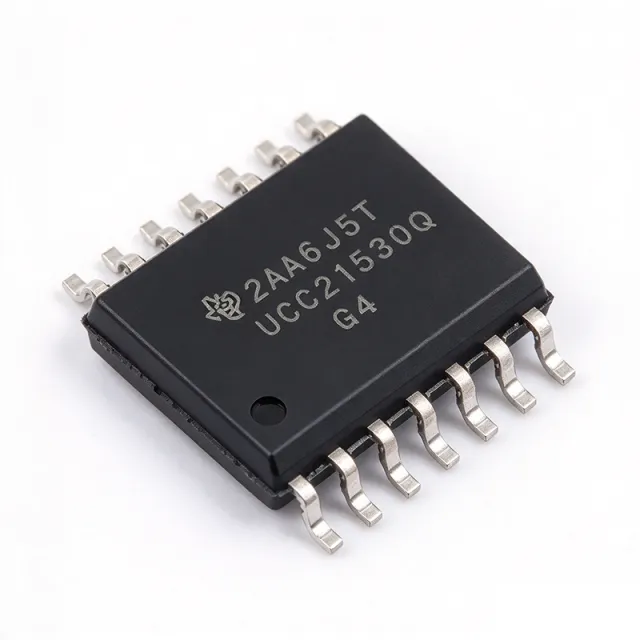
UCC21530QDWKRQ1 - 4A/6A 5.7kVrms Isolated Gate Driver | TI
UCC21530QDWKRQ1 ✓ ActiveSpecification Comparison
| Parameter | UCC21739QDWRQ1 | UCC21530QDWKRQ1 |
|---|---|---|
| Brand | Texas Instruments | Texas Instruments |
| Category | Power MOSFET Drivers | Power MOSFET Drivers |
| Lifecycle Status | Active | Active |
| Stock Status | In Stock | In Stock |
| Unit Price (USD) | $4.52 | $1.07 |
| Product Type | Isolated single-channel gate driver | — |
| Peak Source/Sink Output Current | ±10 A | — |
| Working Voltage (DC link) | Up to 990 V DC | — |
| Isolation Voltage | 3000 V RMS | — |
| Common-Mode Transient Immunity (CMTI) | 100 kV/us minimum | 100 V/ns (minimum) |
| Rise Time (typical) | 33 ns | — |
| Fall Time (typical) | 27 ns | — |
| Miller Clamp Current | 4.5 A | — |
| DESAT Response Time (typical) | 9 us | — |
| Propagation Delay (typical) | [DATA_NEEDED: propagation delay] | — |
| Supply Voltage (VDD/VCC) | 3 V to 5.5 V (logic side), up to 33 V (output side) | — |
| Operating Temperature Range | -40C to +150C (junction) | -40C to +125C |
| Isolation Technology | SiO2 capacitive | — |
| Package | 16-SOIC wide-body (DWR, 7.50 mm width) | 14-pin SOIC (DWK wide-body) |
| Mounting Type | Surface Mount | Surface Mount |
| Automotive Qualification | AEC-Q100 qualified (Q1 suffix) | — |
| Integrated Analog Sense Output | Yes (isolated) | — |
| Function | — | Isolated dual-channel gate driver |
| Number of Channels | — | 2 (high-side / low-side) |
| Peak Source Current | — | 4 A |
| Peak Sink Current | — | 6 A |
| Isolation Voltage (RMS) | — | 5.7 kVRMS |
| Channel-to-Channel Spacing | — | 3.3 mm (minimum) |
| Creepage / Clearance | — | 8.5 mm (DWK wide-body) |
| VDD/VDDA Supply Range | — | 18 V to 25 V (3 V to 18 V on logic side per datasheet) |
| Propagation Delay (Typical) | — | 33 ns |
| Maximum Operating Frequency | — | 5 MHz |
| Programmable Deadtime | — | Yes (DT pin) |
| Enable Pin | — | Yes (active-low) |
| MSL Level | — | 2 |
| AEC-Q100 Qualification | — | Qualified |
| RoHS Status | — | Compliant |
| Logic Input Compatibility | — | CMOS / TTL |