XC7A200T-1FB484C vs XC7A200T-1FBG484I Comparison
Detailed side-by-side comparison of XC7A200T-1FB484C by AMD and XC7A200T-1FBG484I by AMD. Compare key specifications, electrical parameters, packaging, lifecycle status, pricing, and availability to determine the best component for your design requirements.

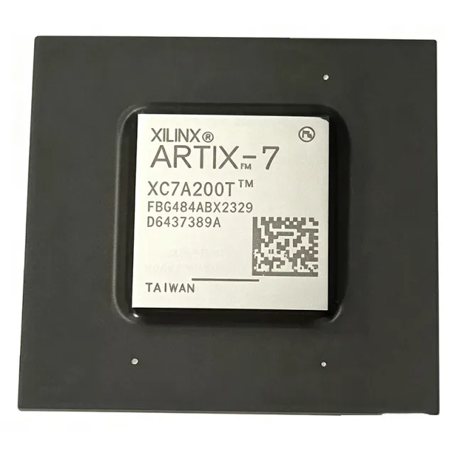
Specification Comparison
| Parameter | XC7A200T-1FB484C | XC7A200T-1FBG484I |
|---|---|---|
| Brand | AMD | AMD |
| Category | FPGA & CPLD | FPGA & CPLD |
| Lifecycle Status | Active | Active |
| Unit Price (USD) | — | $38.50 |
| Device Type | Artix-7 field-programmable gate array | — |
| Logic Cells | 215,360 cells | 215360 |
| User I/O | 285 I/O | 285 |
| DSP Slices | 1,345 slices | 740 DSP48E1 |
| Block RAM | 13,140 Kb | 13 Mb (365 x 36Kb blocks) |
| Speed Grade | Grade 1 | -1 |
| Temperature Grade | Commercial, 0 °C to +85 °C | — |
| Package | 484-ball FCBGA, FB484 | 484-BBGA, FCBGA |
| Mounting Type | Surface mount | — |
| Programmable Logic | Configurable Artix-7 logic architecture | — |
| Embedded Memory | Block RAM and distributed RAM resources | — |
| Signal Processing | Dedicated DSP slice resources | — |
| I/O Standard Support | [DATA_NEEDED: supported I/O standards] | — |
| Configuration Interface | [DATA_NEEDED: configuration interface types] | — |
| Supply Voltage | [DATA_NEEDED: core and I/O supply voltages] | — |
| Maximum Clock Frequency | [DATA_NEEDED: maximum operating clock frequency] | — |
| Operating Temperature | 0 °C to +85 °C | -40C to +100C (Industrial) |
| RoHS Status | Compliant | Compliant |
| REACH Status | Compliant | — |
| Family | — | Artix-7 |
| Logic Slices | — | 33650 |
| I/O Standards | — | LVCMOS, LVDS, HSTL |
| Core Voltage | — | 0.95V to 1.05V |
| Max Clock Frequency | — | 550 MHz |
| Clock Management Tiles | — | 10 CMTs (PLL/MMCM) |
| Ball Pitch | — | 1.0 mm |
| Process Technology | — | 28nm HKMG |
| Configuration Interfaces | — | JTAG, SPI, SelectMAP |