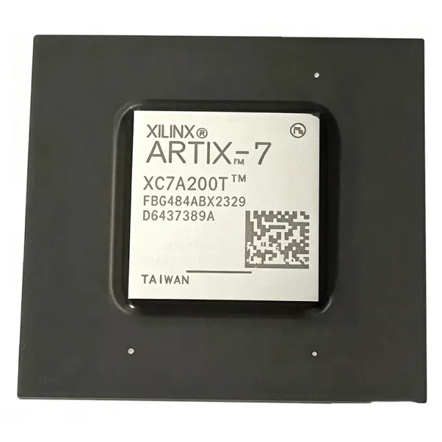
XC7A200T-1FBG484I - 740K Logic Cells FPGA | AMD Xilinx
MPN: XC7A200T-1FBG484I ✓ Active| Qty | Unit Price | Extended |
|---|---|---|
| 1 | $53.21 | $53.21 |
| 10 | $49.5 | $495.00 |
| 100 | $45.8 | $4,580.00 |
| 500 | $42.1 | $21,050.00 |
| 1,000 | $38.5 | $38,500.00 |
XC7A200T-1FBG484I Overview
An FPGA (Field-Programmable Gate Array) is a semiconductor device containing programmable logic blocks and interconnects that can be configured after manufacturing to implement custom digital circuits. FPGAs sit between ASICs (application-specific integrated circuits) and microprocessors in the design hierarchy, offering the flexibility of software-defined hardware with the parallelism of dedicated logic. The Artix-7 family is optimized for cost-sensitive, high-volume applications requiring high logic density and low power, positioned below the Kintex-7 and Virtex-7 families in AMD's 7-series portfolio.
Key features include 285 user I/O pins supporting up to 1.25 Gbps LVDS, 740 DSP48E1 slices with 25x18 multiplier capability, and 10 CMTs providing PLL and MMCM functions. The device also offers 13 Mb of block RAM organized as 365 36Kb blocks, enabling substantial on-chip data storage. The -1 speed grade provides balanced performance with 550 MHz maximum clock frequency, while the industrial temperature range (-40C to +100C) ensures reliable operation in harsh environments.
The XC7A200T-1FBG484I is built on AMD's 28nm high-k metal gate (HKMG) process technology, delivering high performance with low static power. The architecture includes configurable logic blocks (CLBs) with 6-input look-up tables (LUTs), dedicated carry chains for arithmetic functions, and shift register capabilities. The device supports partial reconfiguration, allowing dynamic updates to logic functions without full device reprogramming, which is valuable for adaptive systems.
Typical applications include software-defined radio (SDR), medical imaging, industrial motor control, and high-performance computing acceleration. The high DSP count and low-latency I/O make it ideal for real-time signal processing in communications and defense systems. The 484-ball FBGA package with 1.0mm ball pitch enables compact PCB designs while providing adequate thermal dissipation for moderate power levels.
When designing with this FPGA, ensure adequate decoupling capacitors on all power rails (VCCINT, VCCAUX, VCCO) and follow AMD's PCB design guidelines for high-speed I/O. The configuration interface supports multiple modes including JTAG, SPI, and SelectMAP, allowing flexible system integration. Power sequencing must follow the recommended ramp rates to avoid latch-up or configuration failures.
Drop-in alternatives for XC7A200T-1FBG484I — same package, pin-to-pin compatible. Different-package parts requiring PCB rework are excluded.
Variants in this series
Same-series models that are drop-in compatible with XC7A200T-1FBG484I (same form factor and footprint) — differing in Operating Temperature, Package, Speed Grade.
Quick Comparison Tool — Select alternative parts for side-by-side comparison:
XC7A200T-1FBG484C
✅ Drop-In📋 Reference alternative (not in catalog)
XC7A200T-2FBG484I
✅ Drop-In✓ In Stock
$89.15 / Unit
View Datasheet →XC7A200T-3FBG484E
✅ Drop-In📋 Reference alternative (not in catalog)
XC7A200T-1SBG484I
✅ Drop-In📋 Reference alternative (not in catalog)
XC7A200T-1FBG484I Maximum Ratings & Electrical Characteristics
| Family | Artix-7 |
| Logic Cells | 215360 |
| Logic Slices | 33650 |
| Block RAM | 13 Mb (365 x 36Kb blocks) |
| DSP Slices | 740 DSP48E1 |
| User I/O | 285 |
| I/O Standards | LVCMOS, LVDS, HSTL |
| Core Voltage | 0.95V to 1.05V |
| Speed Grade | -1 |
| Max Clock Frequency | 550 MHz |
| Clock Management Tiles | 10 CMTs (PLL/MMCM) |
| Package | 484-BBGA, FCBGA |
| Ball Pitch | 1.0 mm |
| Operating Temperature | -40C to +100C (Industrial) |
| Process Technology | 28nm HKMG |
| Configuration Interfaces | JTAG, SPI, SelectMAP |
| RoHS Status | Compliant |
XC7A200T-1FBG484I Pin Configuration
| Pin A1 | IO_L1P_T0 — User I/O bank 0, differential pair P |
| Pin A2 | IO_L1N_T0 — User I/O bank 0, differential pair N |
| Pin B1 | VCCINT — Core logic power supply (0.95V-1.05V) |
| Pin B2 | GND — Ground |
| Pin C1 | IO_L2P_T0 — User I/O bank 0, differential pair P |
| Pin C2 | IO_L2N_T0 — User I/O bank 0, differential pair N |
| Pin D1 | VCCAUX — Auxiliary power supply (1.8V) |
| Pin D2 | GND — Ground |
| Pin E1 | IO_L3P_T0 — User I/O bank 0, differential pair P |
| Pin E2 | IO_L3N_T0 — User I/O bank 0, differential pair N |
| Pin F1 | VCCO_0 — I/O bank 0 power supply |
| Pin F2 | GND — Ground |
Typical Applications
XC7A200T-1FBG484I is suitable for 6 applications: Software-Defined Radio (SDR), Medical Imaging, Industrial Motor Control, High-Performance Computing Acceleration, Defense and Aerospace Systems, Video and Image Processing.
Software-Defined Radio (SDR)
The XC7A200T-1FBG484I excels in SDR systems due to its 740 DSP48E1 slices and 13 Mb block RAM, enabling complex digital down-conversion and modulation algorithms. The 285 user I/O pins support high-speed ADC/DAC interfaces up to 1.25 Gbps LVDS, while the 10 CMTs provide precise clock generation for multi-channel operation. The industrial temperature range ensures reliable performance in field-deployed communication equipment.
Recommended
Medical Imaging
In medical imaging systems like ultrasound and CT scanners, the XC7A200T-1FBG484I provides the parallel processing power needed for real-time image reconstruction. Its 740 DSP slices handle beamforming and filtering operations, while the 13 Mb block RAM stores intermediate image data. The 28nm process technology minimizes power dissipation, critical for portable medical devices. The industrial temperature range supports operation in clinical environments.
Recommended
Industrial Motor Control
The XC7A200T-1FBG484I enables high-performance motor control with its 740 DSP48E1 slices for implementing complex FOC (Field-Oriented Control) algorithms. The 285 I/O pins interface directly with PWM drivers and encoders, while the 10 CMTs generate precise timing signals. The -40C to +100C temperature range suits harsh factory environments. The FPGA's deterministic timing ensures consistent control loop performance.
Recommended
High-Performance Computing Acceleration
The XC7A200T-1FBG484I accelerates compute-intensive workloads with its 740 DSP slices and 215,360 logic cells. It implements custom arithmetic pipelines for applications like financial modeling and scientific simulation. The 13 Mb block RAM reduces external memory traffic, while the 1.25 Gbps LVDS I/O enables high-bandwidth data exchange with host processors. The 28nm process balances performance and power efficiency.
Recommended
Defense and Aerospace Systems
The XC7A200T-1FBG484I meets the demanding requirements of defense and aerospace applications with its industrial temperature range and robust 28nm process. The 740 DSP slices handle radar signal processing and electronic warfare algorithms, while the 285 I/O pins interface with various sensors and communication links. The FPGA's reconfigurability allows field updates to adapt to evolving mission requirements.
Recommended
Video and Image Processing
The XC7A200T-1FBG484I processes high-resolution video streams with its 740 DSP slices and 13 Mb block RAM. It implements real-time filters, scaling, and compression algorithms for applications like surveillance and broadcasting. The 285 I/O pins support multiple video interfaces including LVDS and HSTL. The 10 CMTs generate pixel clocks for various video standards, ensuring synchronized output.
Recommended
Recommended Products Summary
Engineering reference data for XC7A200T-1FBG484I — comparison, design guidance, and compliance information.
Selection Guide
Comparison with Alternatives
| Parameter | This Product | XC7A200T-1FBG484C | XC7A200T-2FBG484I | XC7A200T-3FBG484E | XC7A200T-1SBG484I |
|---|---|---|---|---|---|
| Package | 484-BBGA, FCBGA | 484-BBGA, FCBGA - same | 484-BBGA, FCBGA - same | 484-BBGA, FCBGA - same | 484-BBGA, FCBGA - same |
| Brand | AMD | AMD | AMD | AMD | AMD |
| Logic Cells | 215360 | 215360 | 215360 | 215360 | 215360 |
| DSP Slices | 740 | 740 | 740 | 740 | 740 |
| Block RAM | 13 Mb | 13 Mb | 13 Mb | 13 Mb | 13 Mb |
| User I/O | 285 | 285 | 285 | 285 | 285 |
| Speed Grade | -1 | -1 | -2 | -3 | -1 |
| Temperature Range | -40C to +100C | 0C to +85C | -40C to +100C | 0C to +100C | -40C to +100C |
Key Differentiators
- Industrial temperature range (vs XC7A200T-1FBG484C)
- Balanced speed grade (vs XC7A200T-2FBG484I)
- High DSP density (vs XC7A200T-1SBG484I)
Design Notes
The XC7A200T-1FBG484I requires multiple power rails: VCCINT at 0.95V-1.05V, VCCAUX at 1.8V, and VCCO for each I/O bank. Use low-impedance power distribution with dedicated voltage regulators for each rail. Follow AMD's recommended power sequencing: VCCINT first, then VCCAUX, then VCCO. Inadequate decoupling on VCCINT can cause configuration failures.
Place 0.1uF and 1uF decoupling capacitors close to each power pin on the 484-ball FCBGA package. Use a 4-layer or more PCB stackup with dedicated power and ground planes. For high-speed I/O, maintain controlled impedance traces and minimize via stubs. Follow AMD's PCB design guidelines in UG475 for optimal signal integrity.
The 484-ball FCBGA package has a thermal resistance of approximately 8-10 C/W (theta_JA) depending on airflow. At typical power dissipation of 5-10W, ensure adequate airflow or a heatsink to keep junction temperature below 100C. The industrial temperature range allows operation up to 100C ambient, but derating may be required at high utilization.
Compliance Information
RoHS compliant per distributor listings. Not AEC-Q100 qualified as it is an FPGA, not an automotive-grade component.
