XC7K325T-2FFG676I vs XC7K325T-3FFG676E Comparison
Detailed side-by-side comparison of XC7K325T-2FFG676I by AMD and XC7K325T-3FFG676E by AMD. Compare key specifications, electrical parameters, packaging, lifecycle status, pricing, and availability to determine the best component for your design requirements.
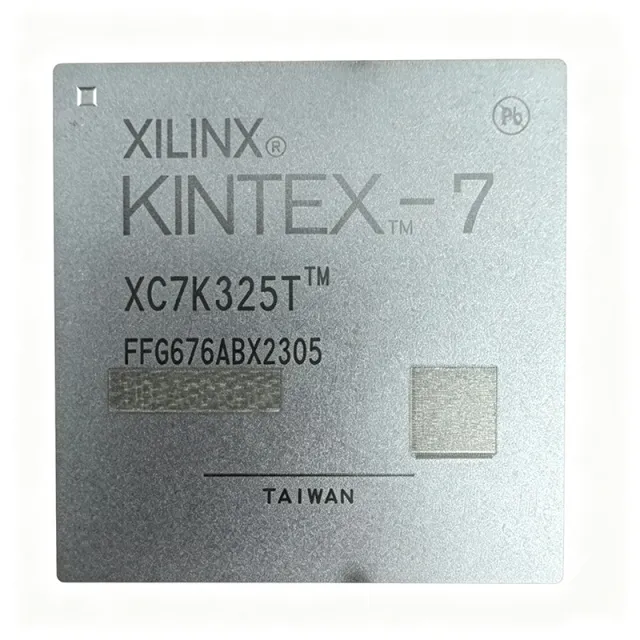

Specification Comparison
| Parameter | XC7K325T-2FFG676I | XC7K325T-3FFG676E |
|---|---|---|
| Brand | AMD | AMD |
| Category | FPGA & CPLD | FPGA & CPLD |
| Lifecycle Status | Active | Active |
| Unit Price (USD) | $98.00 | — |
| Family | Kintex-7 | — |
| Number of Logic Elements/Cells | 326080 | — |
| Number of LABs/CLBs | 25475 | — |
| Total RAM Bits | 16404480 | — |
| Number of I/O | 400 | — |
| Number of DSP Slices | 840 | — |
| Voltage - Supply | 0.97V ~ 1.03V | — |
| Maximum Operating Frequency | 470.37 MHz | — |
| Package / Case | 676-BBGA, FCBGA | — |
| Mounting Type | Surface Mount | Surface mount |
| Operating Temperature | -40°C ~ 100°C (TJ) | — |
| Speed Grade | -2 | -3 |
| Number of Transceivers | [DATA_NEEDED: Number of Transceivers] | — |
| Number of MMCM/PLL | 10 MMCM, 4 PLL | — |
| RoHS Status | Compliant | — |
| Device Type | — | Kintex-7 FPGA |
| Logic Cells | — | 326,080 cells |
| Block RAM | — | 16,020 Kb |
| User I/O | — | 250 I/O |
| Total I/O | — | 400 I/O |
| Process Technology | — | 28 nm |
| Core Voltage Range | — | 970 mV to 1.03 V |
| Clocking Resources | — | MMCM and PLL |
| Maximum Frequency | — | 741 MHz |
| Package | — | FCBGA-676 |
| Ball Count | — | 676 balls |
| Product Family | — | Kintex-7 |
| Supported High-Speed Interfaces | — | PCIe Gen3 and 10 Gigabit Ethernet |
| Programming | — | FPGA configuration |
| RoHS | — | Compliant |
| REACH | — | [DATA_NEEDED: REACH compliance status] |
| AEC-Q100 Qualification | — | [DATA_NEEDED: AEC-Q100 qualification status] |