XCKU5P-1FFVB676E vs XCKU5P-2FFVB676I Comparison
Detailed side-by-side comparison of XCKU5P-1FFVB676E by AMD and XCKU5P-2FFVB676I by AMD. Compare key specifications, electrical parameters, packaging, lifecycle status, pricing, and availability to determine the best component for your design requirements.

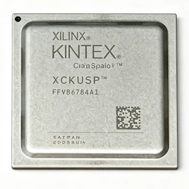
Specification Comparison
| Parameter | XCKU5P-1FFVB676E | XCKU5P-2FFVB676I |
|---|---|---|
| Brand | AMD | AMD |
| Category | FPGA & CPLD | FPGA & CPLD |
| Lifecycle Status | Active | Active |
| Unit Price (USD) | — | $1,660.00 |
| Device Type | Kintex UltraScale+ Field Programmable Gate Array | — |
| Logic Cells | 474,600 cells | 474600 |
| User I/O | 280 I/O | 280 |
| Block RAM | 17,280 Kb | 41984000 bits |
| DSP Slices | 1,824 slices | — |
| Process Technology | FinFET | 16 nm FinFET |
| Speed Grade | -1 | -2 |
| Temperature Grade | Extended | — |
| Junction Temperature Range | 0°C to 100°C | — |
| Package Type | 676-FCBGA | — |
| Package Dimensions | 27 x 27 mm | — |
| Package Pin Count | 676 balls | — |
| Mounting Type | Surface Mount | Surface Mount |
| Product Family | Kintex UltraScale+ | — |
| Programmable Logic | FPGA | — |
| RoHS Status | [DATA_NEEDED: RoHS status] | Compliant |
| REACH Status | [DATA_NEEDED: REACH status] | — |
| AEC-Q100 Qualification | [DATA_NEEDED: AEC-Q100 qualification] | — |
| Lead-Free Status | [DATA_NEEDED: lead-free status] | — |
| Packaging Type | [DATA_NEEDED: shipping package type] | — |
| Standard Packaging Quantity | [DATA_NEEDED: standard packaging quantity] | — |
| Family | — | Kintex UltraScale+ |
| System Logic Cells | — | 474600 |
| Maximum Internal Clock Frequency | — | 725 MHz |
| Core Supply Voltage | — | 825 mV to 876 mV |
| Clock Management | — | MMCM, PLL |
| Package | — | 676-BBGA, FCBGA (FFVB676) |
| Terminal Form | — | Ball |
| Operating Temperature | — | -40C to +100C (Industrial) |
| Temperature Grading | — | Industrial (I) |