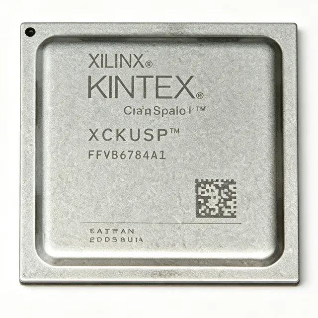
XCKU5P-2FFVB676I - Kintex UltraScale+ FPGA 474K LC | AMD
MPN: XCKU5P-2FFVB676I ✓ Active| Qty | Unit Price | Extended |
|---|---|---|
| 1 | $2100 | $2,100.00 |
| 10 | $1980 | $19,800.00 |
| 100 | $1860 | $186,000.00 |
| 500 | $1760 | $880,000.00 |
| 1,000 | $1660 | $1,660,000.00 |
XCKU5P-2FFVB676I Overview
An FPGA is an integrated circuit that designers configure after manufacturing - hence field-programmable. FPGAs sit within the programmable logic device (PLD) family alongside CPLDs and form the heart of modern adaptive computing systems, providing arrays of programmable logic blocks, routing fabric, and I/O banks that enable highly parallel hardware acceleration. They are frequently used where ASIC cost or inflexibility cannot be justified.
Key features of the XCKU5P include support for 725 MHz internal clocking, MMCM and PLL clock-management tiles, and core operation from 825 mV to 876 mV. The -2 speed grade balances maximum fabric performance against dynamic power, and the industrial rating (-40C to +100C junction) suits harsh deployments.
Technically, the Kintex UltraScale+ family is built on a 16nm FinFET process delivering approximately 1.5x better performance-per-watt than the previous 20nm UltraScale generation. The device integrates high-speed serial transceivers, PCIe Gen3/4 hard blocks, and 100G Ethernet MAC capability, supporting high-bandwidth connectivity and partial reconfiguration for dynamic logic updates without system power-down.
Typical applications include wired and wireless communications infrastructure, data center acceleration, video and image processing, and aerospace and defense systems where logic density plus low power are decisive.
Designers should pay careful attention to power integrity: the 0.85 V typical core rail demands a clean, low-noise supply with dedicated power planes and extensive decoupling, and thermal dissipation under high utilization must be budgeted via the FCBGA thermal path.
This page synthesizes distributor pricing, verified drop-in same-family alternatives, and practical design guidance not found in the manufacturer datasheet alone.
Drop-in alternatives for XCKU5P-2FFVB676I — same package, pin-to-pin compatible. Different-package parts requiring PCB rework are excluded.
Quick Comparison Tool — Select alternative parts for side-by-side comparison:
XCKU5P-1FFVB676I
✅ Drop-In ⚠️ Specs Unverified📋 Reference alternative (not in catalog)
XCKU5P-1FFVB676E
✅ Drop-In ⚠️ Specs Unverified📋 Reference alternative (not in catalog)
XCKU5P-2FFVB676ES
✅ Drop-In ⚠️ Specs Unverified📋 Reference alternative (not in catalog)
XCKU5P-3FFVB676I
✅ Drop-In ⚠️ Specs Unverified📋 Reference alternative (not in catalog)
XCKU5P-2FFVB676N
✅ Drop-In ⚠️ Specs Unverified📋 Reference alternative (not in catalog)
XCKU5P-2FFVB676I Maximum Ratings & Electrical Characteristics
| Family | Kintex UltraScale+ |
| Logic Cells | 474600 |
| System Logic Cells | 474600 |
| Block RAM | 41984000 bits |
| User I/O | 280 |
| Maximum Internal Clock Frequency | 725 MHz |
| Core Supply Voltage | 825 mV to 876 mV |
| Speed Grade | -2 |
| Clock Management | MMCM, PLL |
| Process Technology | 16 nm FinFET |
| Package | 676-BBGA, FCBGA (FFVB676) |
| Terminal Form | Ball |
| Mounting Type | Surface Mount |
| Operating Temperature | -40C to +100C (Industrial) |
| Temperature Grading | Industrial (I) |
| RoHS Status | Compliant |
XCKU5P-2FFVB676I 676-bbga, fcbga (ffvb676) Pin Configuration Guide
Pin configuration for XCKU5P-2FFVB676I (676-bbga, fcbga (ffvb676) package). This digital IC includes GPIO, communication interfaces (UART, SPI, I2C), and power pins. Refer to the manufacturer datasheet for alternate pin functions and configuration options. Essential for embedded system design and PCB layout.

No detailed pinout data available for XCKU5P-2FFVB676I.
Refer to the datasheet for full pin configuration.
Typical Applications
XCKU5P-2FFVB676I is suitable for 6 applications: Data Center Acceleration, Wired Networking Line Cards, Video and Image Processing, Aerospace and Defense Processing, Test and Measurement Instrumentation, Industrial Automation and Machine Vision.
Data Center Acceleration
The XCKU5P-2FFVB676I fits data center acceleration cards where 474,600 logic cells and 41,984,000 bits of block RAM provide enough on-chip buffering for deep pipelines and large lookup tables. Hardened PCIe Gen3/4 blocks give direct host connectivity at up to 16 GT/s per lane without consuming fabric resources, while 100G Ethernet MAC capability supports network-attached accelerators. Deployed between a PCIe edge connector and DDR4 memory controllers, the device delivers deterministic latency that GPUs cannot match for packet processing and regex-style workloads. The 16nm FinFET process improves performance-per-watt roughly 1.5x over the prior generation, reducing cooling budgets in dense 1U servers. Power analysis with Vivado should size the 0.85 V core rail for worst-case utilization before card tape-out.
Recommended
Wired Networking Line Cards
For 100G-class networking line cards, the XCKU5P-2FFVB676I combines high-speed serial transceivers, hardened 100G Ethernet MACs, and 280 user I/Os in one 16nm FinFET device, making it well suited for MAC-layer processing, traffic management, and framing. The 725 MHz-class fabric sustains deep packet-processing pipelines, and 41,984,000 block RAM bits hold flow tables and per-queue buffering. Placed behind a PHY and ahead of a switch ASIC, the FPGA adds programmable protocol agility without a full ASIC NRE. Partial reconfiguration allows updating forwarding logic in the field without powering down the card - a key benefit for carrier equipment. The industrial -40C to +100C rating also covers uncooled outside-plant and central-office thermal environments.
Recommended
Video and Image Processing
Broadcast and machine-vision systems benefit from the XCKU5P-2FFVB676I's combination of 474,600 logic cells for multi-stream 4K pipelines and 41,984,000 bits of block RAM for frame buffers and line delays. Parallel DSP slices sustain color-space conversion, scaling, and convolution at real-time video rates, while transceivers interface to SDI, HDMI-legacy serial, and camera-link-class links. Unlike fixed ASSP solutions, the fabric allows custom merge of ISP blocks per customer. The device sits between video input receivers and output encoders, with DDR4 controllers via the memory interface for off-chip frame storage. The 676-ball FCBGA's high ball count accommodates the wide parallel video buses plus control I/Os within the 280 user I/O budget.
Recommended
Aerospace and Defense Processing
The XCKU5P-2FFVB676I serves radar front-end processing, software-defined radio, and secure communications equipment where the industrial -40C to +100C rating and 16nm FinFET low power matter. With 474,600 logic cells implementing FFTs, filters, and beamforming, and 725 MHz-class clocking, the device handles wideband signal chains that discrete DSPs cannot match in throughput. High-speed transceivers connect data converters directly via JESD204-class links. Designers targeting defense programs should evaluate AMD XQ ruggedized package variants when the program requires XQ qualification - the standard -I device suits industrial-grade platforms, while XQ parts carry extended screening per AMD ruggedized documentation. Partial reconfiguration supports in-field mission-mode updates without system downtime.
Recommended
Test and Measurement Instrumentation
Oscilloscope, logic analyzer, and arbitrary-waveform platforms use the XCKU5P-2FFVB676I for real-time trigger engines, high-speed data capture, and protocol decode. The 280 user I/Os interface multichannel front ends, 41,984,000 block RAM bits buffer deep acquisition records, and hardened PCIe Gen3/4 streams data to a host processor. The 725 MHz-class fabric and parallelism sustain sample-rate-domain processing that a CPU cannot achieve. Placed between the analog front-end digitizers and the processing host, the FPGA defines instrument responsiveness and channel density. Vivado timing constraints should target worst-case industrial corner (-40C to +100C) so bench-to-field behavior stays deterministic, and the 0.85 V core rail needs tight point-of-load regulation for low jitter on capture clocks.
Recommended
Industrial Automation and Machine Vision
Factory automation systems requiring deterministic, high-throughput image processing and real-time control exploit the XCKU5P-2FFVB676I's parallel fabric: 474,600 logic cells implement multi-camera vision pipelines, and 280 user I/Os interface industrial Ethernet PHYs, encoders, and sensor arrays. The industrial -40C to +100C temperature grade tolerates plant-floor thermal swings, and 16nm FinFET efficiency keeps fanless enclosure designs viable. Compared to CPU-plus-vision-software stacks, the FPGA delivers microsecond-level deterministic latency for inline quality inspection. Partial reconfiguration enables product-line changeovers by swapping the vision pipeline at runtime while the control logic stays live. Memory interface to DDR4 supports multi-frame inspection buffering on high-speed conveyor lines.
Recommended
Recommended Products Summary
Engineering reference data for XCKU5P-2FFVB676I — comparison, design guidance, and compliance information.
Selection Guide
Comparison with Alternatives
| Parameter | This Product | XCKU5P-1FFVB676I | XCKU5P-1FFVB676E | XCKU5P-2FFVB676ES | XCKU5P-3FFVB676I |
|---|---|---|---|---|---|
| Package | 676-BBGA, FCBGA (FFVB676) | 676-BBGA, FCBGA (FFVB676) - same | 676-BBGA, FCBGA (FFVB676) - same | 676-BBGA, FCBGA (FFVB676) - same | 676-BBGA, FCBGA (FFVB676) - same |
| Brand | AMD (Xilinx) | AMD (Xilinx) | AMD (Xilinx) | AMD (Xilinx) | AMD (Xilinx) |
| Logic Cells | 474600 | 474600 | 474600 | 474600 | 474600 |
| Block RAM (bits) | 41984000 | 41984000 | 41984000 | 41984000 | 41984000 |
| User I/O | 280 | 280 | 280 | 280 | 280 |
| Speed Grade / Max Clock | -2 / 725 MHz | -1 / lower fabric frequency | -1 / lower fabric frequency, extended temp | -2 ES / 725 MHz (early silicon errata) | -3 / higher fabric frequency |
| Core Supply Voltage | 825 mV to 876 mV | 825 mV to 876 mV | 825 mV to 876 mV | 825 mV to 876 mV | 825 mV to 876 mV |
| Temperature Grade | Industrial (-40C to +100C) | Industrial (-40C to +100C) | Extended (E) | Engineering sample qualification | Industrial (-40C to +100C) |
Key Differentiators
- Best price/performance/watt in mid-range Kintex UltraScale+ family (vs XCKU9P-class devices)
- Highest timing margin in the FFVB676 footprint (vs XCKU5P-1FFVB676I)
- Industrial temperature rating for harsh environments (vs XCKU5P-1FFVB676E)
- Trade-off: higher speed grade cost (vs XCKU5P-1FFVB676I)
Design Notes
The core rail window is only 825 mV to 876 mV - a 51 mV span - so use a point-of-load switching regulator with remote sense and tight output tolerance (better than +/-2%). Add a dedicated core power plane with an array of ceramic decoupling capacitors (mix of 100 nF, 10 uF, 47 uF) placed directly under the FCBGA via fanout. Use AMD Vivado power analysis plus the XPE estimator to size each rail at worst-case utilization; underestimating core current is the most common cause of brown-out during high-activity bursts.
Estimated: at roughly 10 W typical dynamic power in a heavily utilized design, a 676-ball FCBGA without adequate heatsinking can push junction temperature well above the +100C industrial limit in a 55C ambient. Budget a heatsink or cold plate with defined thermal interface material, and verify with the AMD thermal design guidance in the package thermal characteristics documentation. Keep high-activity clock regions away from the package center where the thermal gradient is steepest, and confirm junction temperature margin in Vivado power/thermal reports.
The FFVB676 footprint uses fine-pitch balls and requires controlled-impedance stackup with microvias for escape routing of 280 user I/Os plus transceiver lanes. Follow AMD UltraScale+ PCB design user guide rules for transceiver pair length matching (intra-pair skew tolerance per the guide) and reference-plane continuity under high-speed nets. Download the official UltraScale package pinout files (TXT/CSV per UG575) from AMD developer resources and import them directly into your PCB tool to eliminate manual pinout transcription errors.
Confirm device availability across the full program lifetime before locking the BOM - UltraScale+ devices are subject to allocation cycles. If a substitution is needed, stay within the XCKU5P FFVB676 same-package family (speed or temperature grade changes) so the PCB footprint is preserved; cross-density moves such as XCKU9P require full board redesign. Also confirm your Vivado edition license covers UltraScale+ before scheduling the design cycle.
Compliance Information
RoHS compliant per AMD standard packaging for Kintex UltraScale+ commercial/industrial devices. XQ ruggedized reference information in AMD documentation applies only to XQ packages. AEC-Q100 not applicable to FPGA product class; verify automotive suitability separately with AMD.







