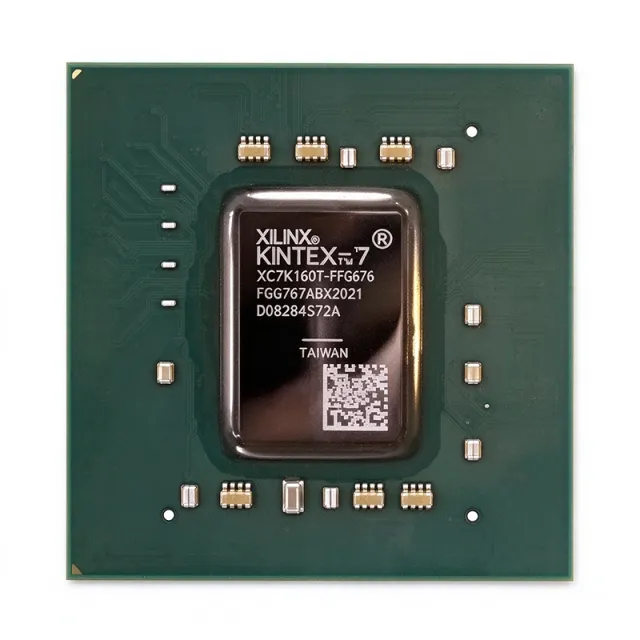
The AMD Xilinx XCKU035-1FBVA676C is a Kintex UltraScale FPGA built on TSMC's 20nm planar CMOS process, integrating 444,343 logic cells, 19,456,000 system gates, 240 DSP48E2 slices, 2,160 Kb of block RAM, and 4.7 Mb of distributed RAM in a 27 mm × 27 mm, 676-ball FCBGA package. The -1 speed grade targets up to 630 MHz fabric performance at a 0.95 V core voltage, with 312 user I/Os, DDR4 memory interface support up to 1,250 Mbps, hardened PCIe Gen3, and 12.5 Gb/s-class GTH transceivers. The commercial (C) temperature grade operates from 0 °C to +85 °C. The part is active in lifecycle status, stocked at 6,000 units with MOQ 1, priced at $584.58 per unit at qty 1 and $467.66 at 1,000 pieces as of 2026-10-19. This guide covers how to design the part in, which pin-compatible alternatives to consider, and what buyers should watch in 2026.
What Are the Quick Answers on the XCKU035-1FBVA676C?
The XCKU035-1FBVA676C sits in the mid-density class of AMD's Kintex UltraScale portfolio, above the XCKU025 and below the XCKU040 and XCKU060. Its defining trade: enough logic and DSP throughput for baseband, SDR, video, and PCIe accelerator workloads, in a footprint compact enough for a half-height, half-length PCIe card. The FBVA676 ballout is shared across the XCKU035 speed grades and the larger XCKU040/XCKU060 in the same package, which matters when you build an upgrade path into your PCB. Key verified figures engineers should anchor on: 444,343 logic cells, 240 DSP48E2 slices, 312 user I/Os, 630 MHz maximum fabric frequency on -1 speed grade, 0.95 V VCCINT, and commercial 0 °C to +85 °C operation. Availability is strong today: 6,000 units in stock at XAIPART, same-day dispatch on stocked lines, with 8–12 week lead times only for non-stocked speed/package combinations.
Takeaway: If your design fits under ~444K cells and 240 DSP slices at -1 speed, this is the cheapest density point on the FBVA676 footprint you can commit to today, with a documented upgrade path in the same ballout.
How Do You Select and Design In the XCKU035-1FBVA676C?
Start with a resource budget. The device gives you 444,343 logic cells organized into CLBs containing two slices of eight 6-input LUTs each, 240 DSP48E2 slices optimized for fixed- and floating-point multiply-accumulate arithmetic, 2,160 Kb of block RAM (540 × 36 Kb blocks), and 4.7 Mb of distributed RAM. If your synthesis estimate consumes more than roughly 70–80% of any resource class, step up to the XCKU040-1FBVA676C, which is pin-compatible with 530,250 logic cells.
Next, validate timing headroom. The -1 speed grade targets up to 630 MHz fabric performance. If your datapath needs more, the -2 grade (up to ~775 MHz) and -3 grade (up to ~860 MHz) ship on the identical FBVA676 footprint, so a speed-grade change does not force a PCB respin.
Then plan the memory subsystem. Hardened PHY blocks support DDR4 up to 1,250 Mbps, and the SelectIO pins also support DDR3, LPDDR3, QDRII+, and RLDRAM3 controllers. For video frame buffering or scratchpad memory beside embedded soft processors, the 2,160 Kb of on-chip BRAM often removes the need for external memory on mid-size designs entirely.
Clock architecture matters at 20nm speeds. The device provides 3 MMCMs and 8 PLLs for clock synthesis and skew management. Budget your clock domains early — with only 3 MMCMs, designs with many independent clock sources should route synthesis-critical domains through the PLL pool.
Power Distribution and PCB Layout
The core runs at 0.95 V VCCINT. Allocate the full power rail set for a Kintex UltraScale BGA design: VCCINT, VCCAUX, VCCO, MGTAVCC, MGTAVTT, VBATT, MGTVCCAUX, VCCADC, VCCBRAM, VCCO_HP, VCCAUX_IO, plus GT helper rails — twelve rail families in total. Follow the package-specific decoupling guidance in UG583 to control simultaneous switching noise (SSN); with 312 user I/Os switching in parallel banks, SSN is the most common root cause of signal-integrity failures on this class of device.
Key Pinout Reference
The verified pinout highlights for power and analog domains on this package include the following functionally critical balls. The complete ball map is in the UG575 FBVA676 package file.
| Ball | Signal | Function |
|---|---|---|
| AF7 | VCCINT | 0.95 V core voltage supply |
| AB12 | VCCAUX | 1.8 V auxiliary supply |
| D14 | VCCO_0 | I/O bank 0 high-performance output supply |
| F4 | IO_L0N_GC_0 | SelectIO, bank 0, general-purpose I/O |
| G6 | IO_L1P_GC_0 | SelectIO, bank 0, general-purpose I/O |
| B11 | MGTAVCC | GT transceiver analog supply, 1.0 V |
| A12 | MGTAVTT | GT transceiver termination supply, 1.2 V |
| Multiple | GND | Common ground (multiple ball positions) |
| Multiple | MGTREFCLK | GT reference clock input (see UG575 FBVA676 file) |
| Multiple | NC | Reserved/no-connect balls per package map |
I/O Standards and Banking
The 312 user I/Os route through SelectIO high-performance buffers supporting single-ended LVCMOS, HSTL, and SSTL, and differential LVDS, RSDS, mini-LVDS, and TMDS standards. Partition I/O banks deliberately: independent banks allow mixed-voltage interfacing, for example a DDR4 PHY on one bank and LVDS ADC/DAC interfaces on another. Keep high-fanout and high-toggle-rate signals on banks close to the ground balls to minimize SSN.
Serial Connectivity
The GTH transceivers run at line rates in the 12.5 Gb/s class and support PCIe Gen3, SATA 3.1, 10GbE KR, and CPRI protocols. The hardened PCIe Gen3 block pairs with the fabric over AXI4 for accelerator workloads. Designers should consult the FBVA676 pinout file and DS890 to confirm the exact GTH channel count exposed by this specific package variant before committing the serial budget.
Takeaway: Commit the 12-rail power tree, decap network per UG583, and bank-level I/O plan before routing; the -1/-2/-3 speed-grade and XCKU040/060 density upgrades all reuse the same PCB.
Which Alternatives and Drop-In Replacements Match the XCKU035-1FBVA676C?
All five verified alternatives below share the same FBVA676 footprint, meaning every option is pin-to-pin compatible — a PCB designed for the XCKU035-1FBVA676C accepts any of them without respin.
| Part Number | Change vs XCKU035-1FBVA676C | Footprint | Best For |
|---|---|---|---|
| XCKU035-1FBVA676I | Industrial temperature: -40 °C to +100 °C vs 0 °C to +85 °C; same silicon, additional test screening | FBVA676, pin-compatible | Aerospace, industrial, extended-temperature builds |
| XCKU035-2FBVA676C | Speed grade -2, up to ~775 MHz (+23% performance vs 630 MHz) | FBVA676, pin-compatible | Designs failing static timing at -1 |
| XCKU035-3FBVA676C | Speed grade -3, up to ~860 MHz (highest) | FBVA676, pin-compatible | Maximum clock frequency headroom |
| XCKU040-1FBVA676C | 530,250 logic cells vs 444,343 (+19% density), same -1 speed grade | FBVA676, pin-compatible | Designs outgrowing the 444K-cell budget |
| XCKU060-1FBVA676C | 725,850 logic cells vs 444,343 (+63% density), same -1 speed grade | FBVA676, pin-compatible | Maximum density on the same board; check DS890 for user I/O bank differences |
Selection logic is straightforward. If the constraint is thermal, choose the -I grade. If the constraint is timing closure, move up speed grades — the -2 grade buys roughly 23% more fabric frequency for a modest premium. If the constraint is logic capacity, the XCKU040 (+19%) or XCKU060 (+63%) upgrades land on the identical ballout; verify I/O bank assignments against DS890 when migrating to XCKU060. If cost is the constraint and your design sits below ~318K cells, the XCKU025 in the same FBVA676 footprint lowers BOM cost — but note it offers fewer DSP slices (150 vs 240) and less block RAM.
Takeaway: Design the PCB once around the FBVA676 ballout and treat speed grade and density as firmware-level sourcing decisions — five verified variants swap without board changes.
Where Does the XCKU035-1FBVA676C Fit in the Market, and What Is the Supply Situation?
Lifecycle status is active per the database. AMD positions Kintex UltraScale as the mid-range tier of the UltraScale portfolio — below Virtex UltraScale in density and bandwidth, above Artix UltraScale in cost and capability — so this part remains a supported, current-generation option in AMD's lineup rather than a legacy pull.
Supply today is healthy: 6,000 units in stock with MOQ 1 as of 2026-10-19, and generally available with same-day shipping from major authorized distributors on stocked lines. Pricing at XAIPART runs from $584.58 at qty 1 down through $555.35 at 10, $526.12 at 100, $496.89 at 500, and $467.66 at 1,000 units, all as of 2026-10-19. Non-stocked speed/package combinations carry typical 8–12 week lead times, which is the number to plan around if your program needs industrial -I variants at volume.
Broader industry context worth monitoring: semiconductor distribution has seen pricing and lead-time volatility across vendors in 2026 — for a parallel example, see XAIPART's coverage of STMicroelectronics raising prices three times in 2026 as STM32 lead times stretch to 52 weeks. Buying ahead of design-freeze milestones is the pragmatic hedge.
Takeaway: Active lifecycle plus 6,000 units on the shelf means no scarcity risk for prototype and early-production builds; lock volume pricing (sub-$468 at 1,000 pcs) before your program scales.
What Trends and Buying Signals Should Engineers Watch in 2026?
Three signals anchored to this part's verified specs and position:
1. Mid-density FPGAs stay the sweet spot for AI-adjacent edge workloads. The 240 DSP48E2 slices and 19.4M system gates make the XCKU035 a natural fit for inference pre-processing, sensor fusion, and video pipelines at the edge — workloads that keep growing. If your utilization estimate approaches 300K cells or your DSP budget tightens, the pin-compatible XCKU040 (530,250 cells) is the no-respin escape hatch. AMD's own framing of the family — best-in-class price/performance/watt at 20nm — is the reason mid-range UltraScale still wins these sockets over full ASIC cycles.
2. Speed-grade flexibility de-risks timing closure late in the project. With -1 (630 MHz), -2 (~775 MHz), and -3 (~860 MHz) all shipping on the identical FBVA676 footprint, treat the speed grade as a schedule hedge: tape out the board on -1 stock, and if static timing analysis fails after place-and-route, a sourcing swap — not a respin — closes the gap. Same-day availability on stocked -1 units makes this a low-friction fallback.
3. Volume buyers should ladder their purchases. The verified tier structure drops $116.92 per unit (20%) from qty 1 to qty 1,000 as of 2026-10-19. With 6,000 units in stock and 8–12 week lead times on non-stocked combinations, a laddered buy — prototype quantities now, production volume booked against the 1,000+ tier — captures the price curve without tying up capital.
For teams also evaluating MCU-class programmable parts for adjacent control logic, XAIPART's STM32F103RET6 engineer's guide and the STM32C5 BOM-cost analysis cover the companion-controller side of a typical FPGA-based system. General sourcing and component research live in the XAIPART component catalog and the XAIPART blog.
Takeaway: Watch your logic/DSP utilization against the 444K-cell ceiling, keep the -2 grade as your timing insurance policy, and ladder purchases against the verified qty-tier curve.
Kommentare
Seien Sie der Erste, der kommentiert.
🔐 Bitte anmelden um einen Kommentar zu veröffentlichen.
Sie haben noch kein Konto? Registrieren