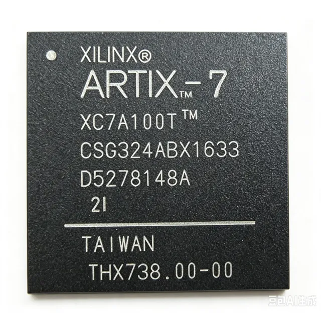
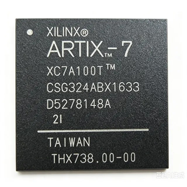
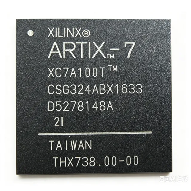
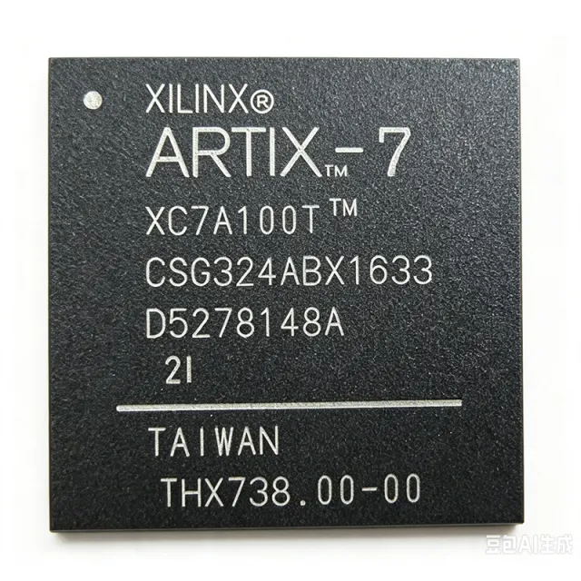
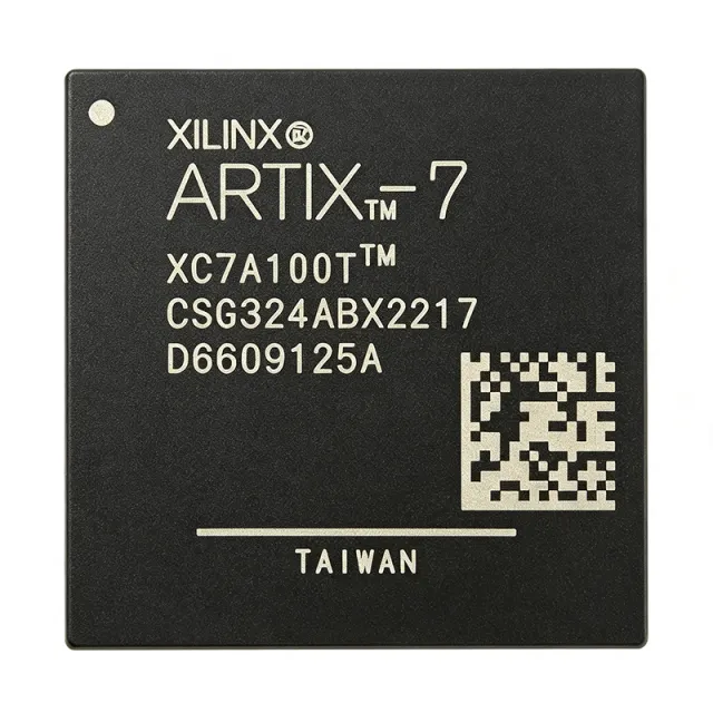
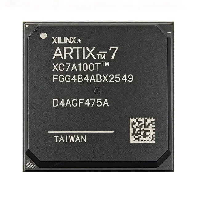
XC7A100T-1FG484I
XC7A100T-1FG484I - 101440-Cell Industrial FPGA | AMD
The AMD XC7A100T-1FG484I is an Artix-7 field-programmable gate array with 101,440 logic cells, 285 I/O, and a 484-BBGA package. It combines programmable logic, block RAM, digital signal processing resources, and programmable I/O in a single surface-mount device, making it suitable for industrial control, communications, instrumentation, embedded processing, and high-performance embedded systems. The -1 designation identifies the device speed grade, while the I suffix identifies the industrial temperature option.
An FPGA is a programmable-logic semiconductor whose digital logic, interconnect, memory, and I/O resources are configured after manufacture. Within the semiconductor hierarchy, an FPGA is a programmable logic device and a complex integrated circuit. Compared with a fixed-function microcontroller or application-specific controller, an Artix-7 FPGA provides parallel processing resources, flexible interfaces, deterministic hardware behavior, and field-updatable configurations. This makes the XC7A100T especially useful when a design requires multiple data paths, high I/O density, or specialized interface timing.
The verified product listing identifies 101,440 programmable logic cells, 285 I/O, and a 484-BBGA package. The device is based on 28 nm CMOS FPGA technology and includes programmable logic, block RAM, DSP resources, clock-management circuitry, and high-speed I/O. Its logic-cell and I/O resources support parallel data acquisition, protocol conversion, control-loop implementation, test sequencing, and embedded signal processing. The listed 1.0 V operating reference provides a basis for power planning, although the complete AC and DC limits must be checked in the manufacturer data sheet for every voltage, temperature, and speed condition.
The FPGA architecture allows multiple clock domains, registered I/O paths, dedicated memory resources, and parallel processing pipelines. DSP blocks can accelerate fixed-point and filtering operations without relying entirely on a soft processor. Dedicated clock-management and I/O resources support predictable timing when constraints, pin planning, and board-level signal integrity are handled according to the AMD design tools and device documentation.
Typical implementations include industrial automation controllers, sensor and instrumentation hubs, communications equipment, data-acquisition systems, embedded vision preprocessing, and custom accelerator modules. The 285 I/O make the device useful for parallel sensor interfaces, digital buses, and control peripherals, while the 101,440 logic cells allow substantial control logic and data pipelines to be implemented on one programmable device.
PCB design must account for the 484-ball package, power-supply sequencing, decoupling, ball assignments, high-speed routing, and thermal performance. Designers should use the AMD package pinout files, verify the exact ball map for the ordered MPN, and generate the physical design using the supported Vivado device installation. Configuration storage, clocking, JTAG access, and power rails should be validated before fabrication.
This product record combines verified distributor specifications, available Artix-7 alternatives, package-level design guidance, and practical selection considerations. It is intended to support initial sourcing and engineering triage, while production decisions should rely on the current AMD data sheet, package files, design guides, and tool release notes.
Angebot
Kontakt