MOSFETs
Produkte (1294)

IRFR5305TRLPBF - -55V P-Channel MOSFET, 31A, 65mΩ | Infineon
The Infineon IRFR5305TRLPBF is a fifth-generation HEXFET P-channel power MOSFET rated for -55V VDS and 31A continuous drain current (Tc), housed in a surface-mount TO-252AA (DPAK) package. It achieves a maximum on-resistance of 65 mΩ at VGS = -10V, leveraging advanced process technology to deliver ultra-low RDS(on) per silicon area and fast switching performance. A P-channel MOSFET is a type of field-effect transistor in which the channel conductivity is controlled by a negative gate-source voltage. P-channel MOSFETs sit in the broader taxonomy: MOSFET -> FET -> transistor -> discrete semiconductor. Because P-channel devices source current when their gate is pulled toward ground, they simplify high-side switching circuits by eliminating the gate-driver charge pump that N-channel high-side switches require, making them favored for load switches, reverse-battery protection, and power-ORing. Key features of the IRFR5305TRLPBF include a -55V drain-source breakdown, 65 mΩ maximum on-resistance, 110W power dissipation (Tc), fast switching speeds, fully avalanche-rated ruggedness, and an ultra-low on-resistance per silicon area achieved through advanced process technology. The P-channel polarity enables high-side switching without level-shifting circuitry, reducing BOM count in battery-powered and industrial systems. Architecturally, the IRFR5305TRLPBF is built on Infineon's HEXFET fifth-generation planar process, which optimizes cell density to minimize RDS(on) while maintaining avalanche ruggedness and low gate charge. The DPAK (TO-252) package exposes the die tab for direct PCB heatsinking, providing low thermal resistance suitable for high-current switching applications. Typical applications include high-side load switching, DC-DC converter synchronous rectifier high-side switches, reverse-polarity battery protection, motor drive half-bridges, and power-ORing circuits. The P-channel topology simplifies gate drive when the load is grounded, which is the canonical configuration for automotive and industrial 12V/24V/48V systems. When designing with this device, calculate conduction loss as I² × RDS(on) and switching loss as ½ × VDS × ID × (tr + tf) × fsw. The TO-252 thermal pad must be soldered to a sufficient copper pour (typically ≥1 in² on FR4) to keep junction temperature below the 175°C maximum rating. Verify avalanche energy (EAS) for any unclamped inductive switching events. This page synthesizes distributor pricing, drop-in alternatives, and practical design notes not found in the manufacturer datasheet.
IRFR5305TRPBF - 55V P-Channel HEXFET MOSFET | Infineon
The Infineon IRFR5305TRPBF is a -55V single P-channel HEXFET power MOSFET, fifth generation HEXFET utilizing advanced processing techniques to achieve extremely low on-resistance per silicon area. This benefit, combined with the fast switching speed and ruggedized device design, gives HEXFET power MOSFETs an excellent efficiency rating in switching applications. The device is housed in a surface-mount DPAK (TO-252AA) package and delivers up to 31A continuous drain current at 25C case temperature with 110W power dissipation. A P-channel power MOSFET is a voltage-controlled semiconductor switch in which the majority carriers are holes, allowing the device to be turned on by pulling the gate voltage below the source. P-channel MOSFETs are commonly used as high-side switches because they can be driven with a simple ground-referenced gate signal, eliminating the need for a bootstrap circuit or charge pump. Within the broader semiconductor taxonomy, the IRFR5305TRPBF belongs to the MOSFET family, then power MOSFET, then P-channel power MOSFET, then discrete semiconductor. Key specifications include a maximum drain-to-source voltage of -55V, maximum on-resistance of 65 mOhm at VGS=-10V, and a typical gate threshold voltage around -2V to -4V. The device is rated for avalanche operation, with a single-pulse avalanche energy of 270 mJ per the Infineon datasheet. Its low RDS(on) and fast switching make it well suited to synchronous rectification, load switching, and motor drive applications in the medium-voltage range. The IRFR5305TRPBF is built on Infineon's IR MOSFET technology platform, which integrates a vertical DMOS structure with advanced cell density to minimize conduction losses. The intrinsic body diode supports synchronous rectification and freewheeling current paths in half-bridge and full-bridge topologies. Logic-level compatibility is achieved at VGS=-10V, while the standard -10V gate drive yields the lowest on-resistance. Typical applications include DC motor control, solenoid and valve drivers, power conversion in industrial 24V-48V bus systems, battery protection and load management, and synchronous rectification in buck and boost converters. The DPAK package offers a low-profile footprint while still allowing substantial copper area for thermal management on the PCB. When designing with this part, ensure that the gate drive circuit can pull the gate to within -10V relative to source for full enhancement, and verify that the avalanche rating is respected during turn-off of inductive loads. Proper PCB layout with a sufficiently large drain copper pour is critical for heat dissipation at high continuous currents. This page synthesizes distributor pricing, drop-in alternatives, and practical design notes not found in the manufacturer datasheet alone, including verified cross-reference equivalents for sourcing flexibility.

IRFR540ZTRLPBF - 100V 35A N-Channel MOSFET | Infineon
The Infineon IRFR540ZTRLPBF is a 100 V, 35 A N-channel power MOSFET built on the company's proprietary IR MOSFET™ advanced process technology, housed in a surface-mount TO-252AA (DPAK) package and supplied on a 13-inch tape-and-reel with 800-piece leader and trailer (TR-L suffix). It is qualified to AEC-Q101 for automotive applications, making it suitable for harsh-environment designs. The device integrates a HEXFET® power stage with extremely low on-resistance per silicon area. Key specifications include a maximum drain-source voltage (VDS) of 100 V, continuous drain current (ID) of 35 A at TC, pulsed drain current of 110 A, and static drain-source on-resistance (RDS(on)) of 28.5 mΩ maximum at VGS = 10 V. The gate charge (Qg) is rated at 39 nC typical. Maximum power dissipation is 91 W at TC, and the operating junction temperature range is -55 °C to +175 °C, exceeding the standard 150 °C industrial limit. The IRFR540ZTRLPBF uses Infineon's advanced planar process technology, optimized for low conduction loss and high repetitive avalanche ruggedness. The 100 V BVDSS rating combined with the 28.5 mΩ on-resistance places this part in the sweet spot for 48 V automotive and industrial switching applications, where it competes directly with similarly rated parts from STMicroelectronics, onsemi, and Vishay. Typical applications include DC-DC converters in automotive ECU power stages, motor drive half-bridges, solenoid and relay drivers, synchronous rectifiers in isolated telecom DC-DC bricks, and high-current hot-swap controllers. The TO-252AA (DPAK) footprint with an exposed drain tab allows efficient PCB-side heat spreading. When designing with this MOSFET, ensure the gate drive swings fully to 10 V for the lowest RDS(on). A gate-source pull-down resistor (10 kΩ minimum) prevents unwanted turn-on during supply transitions. For switching applications above 50 kHz, prioritize minimizing gate-loop and power-loop PCB inductance. This page synthesizes distributor pricing, drop-in cross-brand alternatives, and practical design notes that go beyond the manufacturer datasheet to help engineers select and source this part efficiently.
IRFR540ZTRPBF - 100V N-Ch MOSFET, 35A, DPAK | Infineon
The Infineon IRFR540ZTRPBF is a 100 V N-channel power MOSFET rated for 35 A continuous drain current (at Tc) and 91 W power dissipation, housed in a surface-mount TO-252AA (DPAK) package. Built on Infineon's IR MOSFET technology, it features a maximum on-resistance of 28.5 mOhm at VGS=10V and a total gate charge of 39 nC, making it well suited for high-efficiency switching at moderate frequencies. An N-channel power MOSFET is a voltage-controlled semiconductor switch that uses an insulated gate to modulate current flow between drain and source. When the gate-source voltage exceeds the threshold, a conductive channel forms, allowing current to flow with very low resistance. N-channel MOSFETs sit within the broader hierarchy of discrete semiconductors -> transistors -> MOSFETs -> power MOSFETs, and are the workhorse switching element in DC-DC converters, motor drives, and power-management circuits across industrial, automotive, and consumer systems. Key features include a drain-source breakdown voltage of 100 V, continuous drain current up to 35 A at case temperature, pulsed current capability significantly higher, avalanche-rated body diode for inductive switching, and a logic-compatible gate threshold. The DPAK (TO-252AA) package exposes the drain tab for direct PCB heatsinking, achieving low thermal resistance in a compact surface-mount footprint that is the de-facto industry standard for medium-power applications. The device leverages Infineon's proprietary IR MOSFET cell design, which optimizes the trade-off between on-resistance, switching speed, and avalanche ruggedness. With 28.5 mOhm Rds(on) and 39 nC Qg, conduction and switching losses are balanced for hard-switched topologies operating from single-digit to low-hundred kilohertz. The avalanche-rated intrinsic body diode further allows reliable operation in half-bridge and freewheeling configurations. Typical applications include DC-DC converters (buck and synchronous-rectifier stages), motor-driver H-bridges and half-bridges, solenoid and relay drivers, battery protection circuits, and eMobility auxiliary systems such as 12 V/24 V/48 V load management. The 100 V rating provides comfortable headroom for 24 V industrial buses and 48 V mild-hybrid automotive rails. When designing with this part, prioritize thermal management: the 91 W power rating applies at case temperature, and the DPAK tab must be soldered to a copper pour sized to keep junction temperature below 150 C. For switching applications, keep the gate-drive loop compact to minimize ringing, and add a small gate-source resistor if paralleling multiple devices. This page synthesizes distributor pricing, drop-in alternatives from Infineon and competitors, and practical design notes that complement the manufacturer datasheet rather than restating it verbatim.
IRFR5410TRPBF - -100V P-Channel HEXFET MOSFET, 13A, DPAK | Infineon
The Infineon IRFR5410TRPBF is a P-Channel HEXFET power MOSFET rated at -100 V VDS, -13 A continuous drain current (at Tc), and 205 mΩ maximum on-resistance (VGS = -10 V), housed in a surface-mount TO-252AA (DPAK) package. The part belongs to Infineon's fifth-generation HEXFET family and uses an advanced process technology that achieves ultra-low on-resistance per silicon area, combining fast switching speed with a ruggedized device design that is fully avalanche rated. A MOSFET (Metal-Oxide-Semiconductor Field-Effect Transistor) is a voltage-controlled semiconductor switch used for power switching and amplification. P-Channel MOSFETs conduct when a negative gate-source voltage is applied relative to the source, which is the opposite polarity of N-Channel devices. They are commonly used on the high side of a load to simplify gate drive (the source can be tied to the system positive rail). Within the broader taxonomy, MOSFETs sit under discrete semiconductors, then power transistors, then active components. P-Channel MOSFETs are especially useful in load switching, battery protection, and high-side buck topologies where the system ground must remain stable. Key features of the IRFR5410TRPBF include -100 V drain-source breakdown voltage, 205 mΩ maximum static drain-source on-resistance at VGS = -10 V, total gate charge of 70 nC typical, and a continuous drain current rating of -13 A at TC = 25 °C. The device is fully avalanche rated, supports fast switching, and is offered in an industry-standard DPAK (TO-252) surface-mount footprint. The straight-lead IRFU5410 variant is also part of the same die family. The IRFR5410TRPBF uses an enhanced P-channel cell design that yields extremely low RDS(on) per unit of silicon, supporting efficient power conversion. The low gate charge and ruggedized body diode enable fast switching with reduced switching losses, and the avalanche energy rating allows operation into unclamped inductive loads such as solenoids and motor windings without external protection circuits in many designs. Typical applications include high-side load switching in industrial controls, battery polarity protection and reverse-polarity protection circuits, motor drive and solenoid drivers, DC-DC converters as a synchronous high-side switch, and power-OR-ing in redundant supplies. The P-channel topology simplifies gate drive when the load is tied to system ground. When designing with this part, ensure the gate-source voltage stays within the maximum VGS rating (±20 V absolute) and provide a pull-up resistor on the gate to keep the device off when the controller is in reset. Verify SOA against the application load profile, especially for linear-mode or inrush events, and confirm that the DPAK footprint copper-pour area provides sufficient thermal relief for the worst-case dissipation. This page synthesizes distributor pricing, drop-in alternatives, and practical design notes not found in the standalone manufacturer datasheet, helping engineers evaluate the IRFR5410TRPBF for new designs and pin-compatible replacements.
IRFR5410TRRPBF - P-CH 100V 13A HEXFET MOSFET | Infineon
The Infineon IRFR5410TRRPBF is a P-Channel enhancement-mode power MOSFET built on Infineon's fifth-generation HEXFET technology, rated for -100 V VDS, -13 A continuous drain current (Tc) and 66 W power dissipation (Tc). Housed in a surface-mount TO-252AA (DPAK) package, it delivers an ultra-low on-resistance of 205 mΩ max at VGS = -10 V, making it well-suited to high-efficiency switching and load-switching roles. A power MOSFET (Metal-Oxide-Semiconductor Field-Effect Transistor) is a voltage-controlled semiconductor switch used for switching and amplifying signals in power electronics. P-channel MOSFETs conduct when the gate is pulled below the source, which simplifies high-side switching because the gate drive can be referenced to ground. Within the broader taxonomy, MOSFETs belong to the discrete semiconductor family, which sits under transistors (FETs/MOSFETs), and ultimately under power management and switching conversion. HEXFET is Infineon's proprietary cell architecture that minimizes RDS(on) per unit silicon area. Key features of the IRFR5410TRRPBF include 205 mΩ max on-resistance at VGS = -10 V, fast switching behavior with low gate charge of 70 nC, fully avalanche-rated construction, advanced process technology, and an operating temperature range up to 150 °C junction. The device is supplied on a tape-and-reel packaging suffix and is lead-free (PBF suffix), meeting RoHS requirements. Gate threshold is typically -2 V to -4 V, supporting logic-level gate drivers in some configurations, though -10 V VGS is required to achieve the lowest on-resistance. From an architectural standpoint, the IRFR5410TRRPBF uses a vertical DMOS structure in a P-channel polarity, with the drain connected to the tab of the DPAK package for efficient top-side cooling. Its low gate charge (Qg = 70 nC) keeps driver losses small at high switching frequencies, while its avalanche rating provides ruggedness against inductive transients commonly encountered in motor and solenoid drive circuits. Typical applications include power management in DC-DC converters, load switching, motor control, battery protection, and high-side switching in automotive and industrial systems. It is often deployed as a high-side switch in 48 V telecom rails and as the switching element in polarity-reversal protection circuits. When designing with this part, ensure VGS is driven to at least -10 V for full enhancement, and consider the DPAK's 66 W power rating relative to your thermal design. A low-impedance gate drive and adequate heatsinking are recommended when operating near the maximum current rating. This page synthesizes distributor pricing, drop-in alternatives, and practical design notes not found in the manufacturer datasheet.

IRFR5505TRLPBF - P-Ch 55V 18A 110mOhm DPAK MOSFET | Infineon
The Infineon IRFR5505TRLPBF is a P-Channel enhancement-mode power MOSFET rated at -55 V VDS, -18 A continuous drain current, and 110 mOhm maximum on-resistance, housed in a surface-mount TO-252AA (DPAK) package. It uses Infineon's IR MOSFET™ fifth-generation HEXFET® process to deliver low RDS(on) per silicon area and fast switching, suited for high-efficiency power switching. A power MOSFET (Metal-Oxide-Semiconductor Field-Effect Transistor) is a voltage-controlled semiconductor switch that conducts current between drain and source when the gate is biased. P-channel MOSFETs conduct with the source at a higher potential than the drain, which simplifies high-side load switching by allowing the gate drive to be referenced to ground. The IRFR5505 belongs to the power MOSFET -> discrete semiconductor -> power management hierarchy, and is widely used as a load switch, synchronous rectifier, or low-side/-high-side switch in DC-DC conversion stages. Key specifications include VDS = -55 V, ID = -18 A (Tc), RDS(on) = 110 mOhm max at VGS = -10 V, total gate charge of 21.3 nC, and a continuous power dissipation of 57 W at Tc = 25 °C. The device is rated for an operating junction temperature of -55 °C to +175 °C, and is offered in a lead-free DPAK (TO-252AA) footprint that is footprint-compatible with industry-standard DPAK land patterns. The 'PBF' suffix confirms lead-free / RoHS compliance. The architecture uses Infineon's proprietary HEXFET® cell geometry, a fifth-generation planar stripe layout that minimizes cell pitch while increasing channel density per die area. This translates to low conduction loss and high avalanche ruggedness, with low thermal resistance of approximately 50 °C/W junction-to-case enabling thermal management via the DPAK tab and PCB copper area. The fast switching speed combined with low gate charge makes it suitable for high-frequency PWM stages above 100 kHz. Typical applications include DC-DC converter high-side switches, polarity-reversal protection (ideal-diode OR-ing), load management in battery-powered systems, motor drive H-bridges, and power-rail switching in industrial automation and telecom hardware. It is also commonly deployed in power-OR'ing circuits for redundant supplies and as a synchronous rectifier in low-to-medium power buck converters. When designing with this part, observe the SOA (Safe Operating Area) limits and ensure the gate drive voltage swing (VGS) is sufficient to fully enhance the device. Linear-mode operation above the pulsed current rating will quickly exceed thermal limits; switch-mode operation is recommended for high-current paths. The tab is electrically tied to the drain, so the PCB copper pad must be sized to handle continuous current and thermal dissipation.
IRFR5505TRPBF - P-Channel 55V 18A HEXFET MOSFET | Infineon
The Infineon IRFR5505TRPBF is a P-channel power MOSFET rated at -55 V VDS and -18 A continuous drain current, using Infineon's fifth-generation HEXFET technology in a TO-252AA (DPAK) surface-mount package. It delivers an ultra-low on-resistance of 110 mOhm max at VGS = -10 V and a total gate charge of 21.3 nC, achieving an extremely low RDS(on) per silicon area. A P-channel MOSFET is a type of field-effect transistor in which the conducting channel is formed by positively charged carriers (holes) when a negative gate-source voltage is applied. P-channel devices occupy a distinct branch of the broader MOSFET family (which includes N-channel MOSFETs) within the discrete-semiconductor category, sitting under the wider umbrella of power-switching transistors and semiconductor switches. Their inherent high-side switching simplicity eliminates the charge-pump or bootstrap circuitry required by N-channel devices in many topologies, at the cost of higher RDS(on) for a given die size. Key features include a maximum continuous drain current of -18 A at TC = 25 C, pulsed drain current of -72 A, and a maximum power dissipation of 57 W at TC = 25 C. The TO-252AA package provides a low thermal resistance (junction-to-case) of 2.2 C/W, enabling compact designs without external heatsinking at moderate loads. The device is rated for an operating junction temperature range of -55 C to +175 C and includes an avalanche-rated single-pulse capability. The IRFR5505TRPBF utilizes advanced process technology that combines low on-resistance per silicon area with fast switching speeds and ruggedized device design. This combination provides an extremely efficient and reliable device for use in a wide variety of applications including DC-DC converters, motor drives, and load switching where P-channel high-side switching is preferred. The DPAK package is optimized for surface-mount manufacturing and offers an exposed drain tab that doubles as the thermal pad. Typical applications include high-side load switching in industrial 24V/36V systems, P-channel synchronous rectifier replacements, battery protection and reverse-polarity blocking in portable equipment, and DC motor control. The wide operating voltage range and avalanche ruggedness also suit automotive ECU loads and power-rail OR-ing. When designing with this device, ensure the gate-source voltage stays within the +/-20 V absolute maximum to prevent oxide rupture. Use a gate resistor (typically 10-100 ohm) to limit ringing, and add a TVS or Zener clamp on the gate if the gate drive exceeds +/-20 V during transients. Verify SOA at the operating VDS and ID combination before deployment, particularly when switching inductive loads. This page synthesizes distributor pricing, drop-in same-package alternatives, parametric comparison tables, and practical design notes not found in the manufacturer datasheet alone.
IRFR6215TRLPBF - 150V P-Ch HEXFET MOSFET, 13A, DPAK | Infineon
The Infineon IRFR6215TRLPBF is a -150V single P-channel HEXFET power MOSFET in a TO-252AA (DPAK) surface-mount package rated for 13A continuous drain current at Tc and 110W power dissipation at Tc. Built on Fifth Generation HEXFET technology, it pairs a 580 mOhm maximum on-resistance at VGS = -10V with 44 nC typical total gate charge to deliver low conduction loss and fast switching in high-side and load-switch topologies. A P-channel MOSFET is a voltage-controlled device in which the source and drain terminals carry negative-polarity current relative to the source (the channel conducts when the gate is pulled below the source). MOSFETs sit one level above BJTs in the power-switching taxonomy (MOSFET -> power transistor -> discrete semiconductor) and are favored over BJTs for high-frequency switching because they are voltage-driven rather than current-driven, eliminating continuous base current and dramatically shrinking driver losses. Key features include -150V VDS breakdown that provides generous transient headroom for 48V telecom, industrial bus, and offline-aux rails; an industry-standard DPAK footprint with an exposed drain tab for direct PCB thermal spreading; -20V maximum VGS rating with internal ESD protection; and a 175 C maximum operating junction temperature for harsh-environment survivability. The 580 mOhm maximum RDS(on) at VGS = -10V minimizes conduction loss in steady-state load-switch applications, while 44 nC Qg allows modest gate drivers to switch the device at moderate PWM frequencies. Typical applications include high-side switching in 48V telecom and industrial bus systems, DC load management in battery-powered equipment, polarity-protection and OR-ing circuits, motor brake and slow-decay dissipation, and synchronous-rectifier replacements for PNP pass transistors in linear-regulator upgrades. The Infineon IRFR6215 family uses the same DPAK land pattern as industry-standard N-channel parts, simplifying PCB reuse for designers porting from PNP pass elements to modern MOSFET switches. When designing with this part, observe the VGS rating: the gate must never exceed +/-20V, so a gate-resistor plus optional Zener clamp is recommended when driven by a higher-voltage gate drive. Thermal management requires copper spreading under the drain tab; a minimum 1 square inch of 2 oz copper keeps the junction within safe limits at 2-3W steady dissipation. This page synthesizes distributor pricing, drop-in alternatives, and practical design notes that complement - but do not duplicate - the manufacturer datasheet.
IRFR6215TRPBF - 150V P-Channel HEXFET MOSFET, 13A | Infineon
The Infineon IRFR6215TRPBF is a fifth-generation HEXFET P-channel power MOSFET rated at 150 V VDS, 13 A continuous drain current (Tc), and 110 W power dissipation (Tc), housed in a surface-mount TO-252AA (DPAK) package. This single P-channel device uses Infineon's advanced processing techniques to achieve an extremely low on-resistance per silicon area of 0.295 ohm maximum, balancing conduction loss and switching performance. A P-channel MOSFET (Metal-Oxide-Semiconductor Field-Effect Transistor) is a voltage-controlled device in which the channel is formed by p-type semiconductor material, allowing current to flow when the gate is pulled below the source. P-channel MOSFETs sit in the same taxonomy as their N-channel siblings, both belonging to the power MOSFET > MOSFET > discrete semiconductor > semiconductor hierarchy. P-channel parts are commonly used as high-side switches because they can be driven by a low-side referenced gate signal, simplifying the bootstrap or charge-pump circuitry required by N-channel high-side drivers. Key features include a 0.295 ohm maximum on-resistance at VGS = -10 V, 44 nC total gate charge, fast switching speed, and a ruggedized HEXFET cell design that has been production-proven across multiple generations. The device's 150 V drain-source breakdown provides ample margin for 48 V telecom rails, 60 V industrial bus systems, and offline flyback auxiliary circuits. The DPAK (TO-252AA) surface-mount package exposes the die to a copper tab on the PCB, enabling 110 W dissipation with proper footprint design. The IRFR6215 uses a fifth-generation HEXFET cell with a stripe-cell planar DMOS architecture, providing a strong figure-of-merit (FOM = RDS(on) x Qg) and proven avalanche ruggedness. The gate threshold is specified in the standard -2 V to -4 V range, and the device is fully characterized for both continuous and pulsed operation. The P-channel polarity allows direct high-side switching without a bootstrap circuit, reducing overall BOM count. Typical applications include load switches, power management in industrial and telecom 48 V systems, battery protection circuits, motor drive H-bridges (high-side position), and DC-DC converter synchronous rectifiers. Designers value this part for its balance of voltage rating, current handling, and DPAK footprint compatibility with standard reflow profiles. When designing with this device, ensure that the PCB copper pad under the DPAK tab is sized to handle the desired power dissipation, and that the gate drive is referenced to the source pin (not ground) to maintain proper VGS enhancement. A gate-source resistor of 10 kohm or higher is recommended to prevent inadvertent turn-on from dv/dt-induced Miller coupling. This page synthesizes distributor pricing, drop-in alternatives, and practical design notes not found in the manufacturer datasheet alone, giving engineers a single reference for sourcing and substitution decisions.
IRFR7540TRPBF - 60V 90A 4.8mΩ StrongIRFET N-MOSFET | Infineon
The Infineon IRFR7540TRPBF is a 60 V N-channel StrongIRFET™ power MOSFET rated for 90 A continuous drain current (Tc) and 140 W power dissipation, housed in a surface-mount TO-252AA (DPAK) package. It features an ultra-low maximum on-resistance of 4.8 mΩ at VGS = 10 V, an avalanche-rated rugged body diode, and improved gate, avalanche, and dynamic dV/dt ruggedness per Infineon's HEXFET/StrongIRFET design philosophy. Bond-wire current limit is 90 A by source bonding technology, with ID max reaching 110 A under pulsed conditions limited by TJmax. An N-channel power MOSFET is a voltage-controlled semiconductor switch in which applying a positive gate-to-source voltage creates an inversion layer that conducts current between drain and source. The 'StrongIRFET' technology platform from Infineon targets low-voltage, high-current applications by optimizing the silicon cell density and die size for minimal RDS(on) per unit area. The DPAK (TO-252AA) surface-mount package is the industry-standard footprint for medium-power discrete MOSFETs, sitting in the hierarchy: TO-252 -> DPAK family -> surface-mount power packages. MOSFETs belong to the broader category: transistor -> FET -> power MOSFET -> discrete semiconductor. Key features include 60 V VDS max, 4.8 mΩ RDS(on) max at VGS = 10 V (typical 3.7 mΩ at 100 µA), gate threshold of 3.7 V typical, low gate charge for fast switching, and a rugged avalanche-rated body diode that tolerates unclamped inductive switching events. The combination of low on-resistance and high continuous current makes the IRFR7540TRPBF suitable for high-current switching where conduction losses dominate. The IRFR7540TRPBF uses Infineon's StrongIRFET™ silicon technology, an enhancement-mode N-channel trench MOSFET architecture. The trench-gate structure reduces cell pitch and increases channel density per unit area, directly lowering RDS(on). The die is rated to 175°C maximum junction temperature, and thermal resistance from junction to case (RθJC) is typically around 1°C/W per the DPAK package family, enabling 140 W dissipation when properly mounted on a PCB with sufficient copper area. Typical applications include 48 V buck converters, motor drives and H-bridges, DC-DC synchronous rectification, battery management systems for e-mobility, and high-current load switches in industrial automation. The low RDS(on) keeps conduction losses low in continuous high-current paths. When designing with this device, calculate power dissipation as P = I² × RDS(on) and ensure the PCB copper area keeps junction temperature below 150°C for reliable operation. Use a gate driver capable of sourcing/sinking at least 1 A to switch the gate quickly and minimize transition losses.
IRFR7546TRPBF - 60V StrongIRFET N-MOSFET, DPAK | Infineon
The Infineon IRFR7546TRPBF is an N-channel StrongIRFET power MOSFET rated at 60 V VDS with 7.9 mOhm maximum RDS(on), housed in a surface-mount DPAK (TO-252AA) package. It delivers up to 71 A of drain current (ID max) and 99 W of continuous power dissipation at 25 deg C case temperature, leveraging Infineon's StrongIRFET technology for low conduction loss and high avalanche ruggedness. A power MOSFET is a voltage-controlled semiconductor switch used to efficiently route or regulate current in power conversion circuits. The StrongIRFET family targets high-current DC-DC converters, motor drives, and synchronous rectification where ultra-low RDS(on) and high inrush/short-circuit capability are required. MOSFETs sit within the broader power-semiconductor hierarchy (power MOSFET -> discrete semiconductor -> power management building block) and are usually the workhorse switch on the low-voltage side of a system. The IRFR7546 uses a stripe-cell planar trench-style process optimized for 12 V to 48 V rails. RDS(on) max of 7.9 mOhm at VGS=10 V minimizes I^2R conduction loss, while the 60 V VDS rating provides comfortable derating margin for 24 V industrial buses and 36 V e-mobility packs. Bond-wire current limit is 56 A per source bonding technology (per application note AN-1140), and pulsed drain current is rated higher depending on pulse width and thermal starting conditions. Typical applications include high-current synchronous rectification in switched-mode power supplies, brushed and brushless DC motor drive half-bridges, low-side buck/fet switches, and battery protection disconnect switches. The 60 V rating and DPAK footprint also suit solar charge controllers, e-bike controllers, and low-voltage automotive subsystems (when paired with proper TVS protection). When designing in this part, evaluate SOA against your worst-case pulse profile and follow AN-1140 mounting guidelines for DPAK thermal performance. The exposed tab must be soldered to sufficient copper pour to keep junction temperature within the 175 deg C max rating.
IRFR9024NTRLPBF - 55V P-Channel HEXFET MOSFET | Infineon
The Infineon IRFR9024NTRLPBF is a P-Channel enhancement-mode HEXFET power MOSFET rated at -55 V VDS, -11 A continuous drain current (Tc), and 175 mOhm maximum on-resistance at VGS = -10 V, housed in a surface-mount TO-252AA (DPAK) package with a 38 W power dissipation rating. The part ships on a 13-inch tape-and-reel with left orientation and is built on Infineon's fifth-generation HEXFET process which targets the lowest RDS(on) per silicon area in a P-channel die. The LPBF suffix denotes lead-free, RoHS-compliant terminal finish suitable for modern reflow profiles. The "TRL" infix indicates the specific reel orientation used during automated pick-and-place loading. What is a P-channel power MOSFET? A P-channel MOSFET is a type of field-effect transistor where the channel is formed by holes (positive charge carriers) rather than electrons. P-channel devices use a negative gate-source voltage to turn on and are commonly used as high-side switches because they can be driven directly from a logic-level signal referenced to ground, simplifying gate drive circuitry compared to N-channel high-side switches that require a charge pump or bootstrap. P-channel MOSFETs sit within the broader category of power MOSFETs (MOSFET -> discrete semiconductor -> power transistor) and are essential building blocks in power management, load switching, battery protection, and motor control applications. Key features include an industry-standard DPAK (TO-252) surface-mount footprint, an ultra-low on-resistance per silicon area characteristic of Generation-5 HEXFET technology, fast switching performance for PWM and DC-DC converter topologies, and a ruggedized body diode suitable for inductive loads. The device's enhancement-mode operation requires a negative VGS to conduct, simplifying gate drive in high-side P-channel switch configurations where pulling the gate to ground turns the device on. The IRFR9024NTRLPBF utilizes Infineon's proprietary HEXFET stripe-cell geometry that minimizes cell pitch while maximizing channel density per unit area. This results in the lowest specific on-resistance (RDS(on) x area) in its voltage class, reducing conduction losses and enabling higher current handling or smaller PCB footprint compared to older planar P-channel MOSFETs. Typical applications include high-side load switching in 12 V / 24 V automotive and industrial systems, battery protection and reverse-polarity blocking in portable equipment, DC-DC converter synchronous-rectifier high-side switches, motor driver H-bridges, and power-OR-ing circuits in redundant supply architectures. The -55 V rating comfortably exceeds the maximum nominal rail voltages of 24 V industrial or 12 V automotive systems with substantial transient margin. When designing with this device, ensure that the gate-source voltage stays within the absolute maximum rating of +/-20 V and that the SOA curve is respected during switching transients. A gate pull-up resistor to the source pin ensures the device stays off when the gate driver is in a high-impedance state, preventing accidental turn-on from leakage or dv/dt coupling. This page synthesizes distributor pricing, drop-in alternatives sourced from manufacturer cross-reference data, and practical design notes that go beyond the manufacturer datasheet's parameter tables.
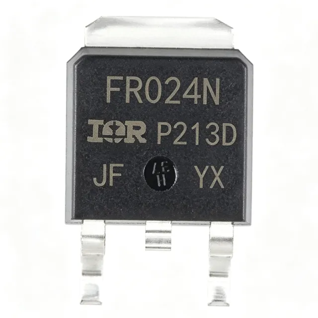
IRFR9024NTRPBF - 55V 11A P-Channel HEXFET MOSFET | Infineon
The Infineon IRFR9024NTRPBF is a fifth-generation P-Channel HEXFET power MOSFET rated for -55V VDS and -11A continuous drain current (Tc) in a surface-mount TO-252AA (DPAK) package. Housed in a 3-pin DPAK outline, it delivers a maximum on-resistance of 175 mOhm at VGS = -10V and a typical total gate charge of 12.7 nC, providing a strong balance between conduction loss and switching speed for low-to-medium frequency power switching. A P-Channel MOSFET (Metal-Oxide-Semiconductor Field-Effect Transistor) is a voltage-controlled majority-carrier device whose carrier polarity is holes (positive charge). P-Channel MOSFETs sit within the broader family of power transistors -> field-effect transistors -> MOSFETs -> discrete semiconductors. They are commonly used as high-side switches where an N-Channel driver would require a charge pump, simplifying gate-drive circuitry in load-switch and battery-protection applications. Key features of the IRFR9024NTRPBF include advanced process technology for low RDS(on) per silicon area, a maximum continuous drain current of -11A at 25C case temperature, 38W maximum power dissipation (Tc), and an avalanche-rated body diode for inductive switching. The device is rated for operating junction temperatures from -55C to +175C, making it suitable for harsh thermal environments. The TO-252AA (DPAK) surface-mount package provides a low thermal resistance path to the PCB copper pad. Architecturally, the IRFR9024NTRPBF uses Infineon's proprietary HEXFET fifth-generation cell structure, which optimizes the trade-off between specific on-resistance and gate charge. The P-Channel die is housed in a standard DPAK outline with the industry-standard pinout of Gate (pin 1), Drain (pin 2, tab), and Source (pin 3), allowing drop-in compatibility with numerous cross-brand equivalents. Typical applications include high-side load switches in industrial control, battery protection and OR-ing in portable equipment, DC fan and motor speed control, power-rail inverters, and general-purpose power management in consumer and automotive 12V/24V subsystems. The P-Channel topology simplifies high-side switching without needing a bootstrap supply. When designing with this part, ensure the gate-source drive provides at least -10V for full enhancement, and keep the dv/dt loop between drain and source compact to limit ringing. The TO-252AA tab must be soldered to a copper pour of at least 1 square inch for the rated 38W power dissipation.
IRFR9120NTRLPBF - 100V P-Channel MOSFET, 6.6A, DPAK | Infineon
The Infineon IRFR9120NTRLPBF is a -100V P-channel power MOSFET built on Infineon's IR MOSFET planar cell technology, rated for -6.6A continuous drain current (Tc) and 40W power dissipation in a 3-pin TO-252AA (DPAK) surface-mount package. It delivers a maximum on-resistance of 480 mOhm at VGS = -10V and a typical gate charge of 18 nC, providing a low-loss switching solution for high-side and load-switch applications. The part ships on 13-inch Tape & Reel with reel left orientation, and is qualified to the automotive-grade IRFR9120N silicon die. A P-channel MOSFET is a type of field-effect transistor in which the conducting channel is formed by positive charge carriers (holes) when a negative gate-to-source voltage is applied. P-channel devices sit in the power-management hierarchy alongside N-channel MOSFETs, IGBTs, and wide-bandgap GaN/SiC switches; they are especially valued in high-side switching because they can be driven directly from a low-voltage logic rail without a charge pump or bootstrap circuit, simplifying gate drive design compared with N-channel high-side switches. Key electrical features of the IRFR9120NTRLPBF include a -100V drain-to-source breakdown (VDS), -6.5A pulsed drain current capability, gate threshold of -2V to -4V, and an avalanche-rated single-pulse body diode. The DPAK package exposes the tab as drain, which doubles as a thermal pad with theta_JC rated to support 40W continuous dissipation when properly soldered to a 1-square-inch copper land. Typical applications include high-side load switching in 24V/48V industrial buses, reverse-battery protection, motor-speed-control low-side stages, DC-DC converter synchronous-rectifier replacements, and automotive relay replacements. The combination of -100V rating and DPAK footprint makes it a direct fit for legacy designs migrating from through-hole TO-220 to surface-mount assemblies. When designing with this MOSFET, ensure the gate-drive pull-up returns to the source pin and that the gate-source resistor (typically 10 kOhm to 100 kOhm) is fitted to prevent unintended turn-on from dv/dt coupling. For switching applications above 100 kHz, verify that the driver's rise/fall time does not violate the dv/dt-induced turn-on rating. This page synthesizes distributor pricing, drop-in alternatives, and practical design notes that are not found in the manufacturer datasheet alone, including verified same-brand and cross-brand pin-compatible replacements in the same TO-252AA footprint.
IRFR9120NTRPBF - 100V P-Channel HEXFET MOSFET, 6.6A | Infineon
The Infineon IRFR9120NTRPBF is a P-Channel power MOSFET rated at -100 V VDS, -6.6 A continuous drain current (at TC), and 40 W power dissipation, supplied in a surface-mount TO-252AA (DPAK) package. It uses Infineon's HEXFET fifth-generation process technology to deliver an ultra-low on-resistance of 480 milliohms maximum and a typical total gate charge of 18 nC, balancing conduction loss with switching speed for medium-power switching applications. The device is supplied on a 13-inch tape-and-reel carrier (TR suffix), Pb-free (PBF suffix), and qualified to MSL1 for unlimited floor-life at the assembler. A P-Channel MOSFET is a type of field-effect transistor in which the body and source terminals are tied together through a P-N junction that is reverse-biased under normal operation. When a negative gate-source voltage is applied, a conductive P-channel inverts at the surface, allowing conventional current to flow from source to drain. P-Channel devices sit at the high-side of a load in low-side switch topologies, simplifying gate drive in systems where the negative rail is the system ground. As a member of the power MOSFET family, P-Channel parts complement their N-Channel counterparts in H-bridges, level shifters, and reverse-polarity protection circuits. Key differentiating features of the IRFR9120NTRPBF include its -100 V drain-source rating that provides substantial margin against 48 V telecom rails and 60 V rectified supplies, an on-resistance of 480 milliohm which keeps conduction loss modest for a 6.6 A device, and a low gate charge of 18 nC that minimizes driver loss at higher switching frequencies. The DPAK (TO-252AA) surface-mount package provides a low thermal resistance of approximately 50 C/W when the tab is soldered to 1 square inch of 2 oz copper, enabling natural-convection cooling at the part's 40 W rating. Architecturally, the IRFR9120NTRPBF is built on Infineon's IR MOSFET cell technology, which uses a vertical DMOS structure with a HEXFET cellular layout to maximize channel width per unit silicon area. The die is housed in a DPAK plastic package with a metal tab acting as the drain terminal, providing both electrical connection and a direct thermal path to the PCB copper pour. The avalanche-rated design ensures the device can absorb unclamped inductive switching transients commonly seen when driving relays, solenoids, or motors. Typical applications include high-side load switching in 24 V and 48 V industrial systems, polarity-reversal protection in battery management circuits, DC motor drive bridges, solenoid and relay drivers, and synchronous rectifier positions in low-frequency buck-derived converters. The part is also commonly used as a high-side switch in audio amplifier muting circuits where its low on-resistance minimizes signal-path loss. When designing with the IRFR9120NTRPBF, ensure that VGS does not exceed the +/-20 V absolute maximum rating and that the gate is driven from a low-impedance source to avoid dv/dt-induced turn-on. The DPAK tab must be soldered to a copper pad of at least 50 mm squared for the device to achieve its rated 40 W dissipation, and a gate-source resistor of 10 kohm is recommended to hold the device off during power-up transitions. This page synthesizes distributor pricing, drop-in alternatives, and practical design notes not found in the manufacturer datasheet.

IRFS3006TRL7PP - 60V 240A N-Ch HEXFET MOSFET | D2PAK-7 | Infineon
The Infineon IRFS3006TRL7PP is a 60 V, 240 A N-channel HEXFET power MOSFET in a surface-mount D2PAK (TO-263, 7-lead) package optimized for high-current synchronous rectification, OR-ing, hot-swap, and motor-drive stages. It is part of Infineon's IR MOSFET family and features an extremely low on-resistance of 1.5 mΩ typical (RDS(on)), a continuous drain current rating of 240 A at Tc, and a pulsed avalanche rating supporting robust operation in demanding switching topologies. A power MOSFET is a voltage-controlled, majority-carrier semiconductor switch that modulates current flow between its drain and source terminals under the control of a gate voltage, making it the fundamental building block of modern DC-DC converters, motor controllers, and load-management circuits. Within the broader taxonomy, this device sits in the N-channel enhancement-mode power MOSFET category, which belongs to discrete power semiconductors and the wider power management ecosystem. The HEXFET cell structure used by Infineon delivers an excellent figure of merit (FOM = RDS(on) × Qg) that minimizes both conduction and switching losses simultaneously. Key features of the IRFS3006TRL7PP include a maximum drain-source voltage (VDS) of 60 V, a gate charge (Qg) of approximately 200 nC for fast switching transitions, and a continuous drain current of 240 A at case temperature (Tc). The 7-lead D2PAK (TO-263) package provides an exposed metal tab that serves as the drain terminal and enables direct PCB heatsink attachment for high-power dissipation up to 375 W. Logic-level-compatible gate drive thresholds simplify interface to standard gate-driver ICs. Architecturally, the IRFS3006TRL7PP uses Infineon's proven planar HEXFET stripe-cell geometry with an intrinsic body diode capable of supporting hardswitched and resonant topologies. The avalanche-rated die supports unclamped inductive switching events, and the optimized body-diode dv/dt immunity suits bridge configurations where reverse recovery must be controlled. Compared with trench MOSFET generations, this planar HEXFET retains a wider safe operating area (SOA) for linear-mode and hot-swap use cases. Typical applications of the IRFS3006TRL7PP include high-current synchronous rectification in server and telecom DC-DC converters, 12 V/24 V automotive ECU and load-switch circuits, hot-swap controllers and OR-ing FETs in redundant -48 V telecom power shelves, battery protection and high-current BMS switching, and brushed/brushless DC motor drive bridges. The D2PAK-7 footprint allows direct substitution for other 60 V-class HEXFETs in existing layouts. When designing with this part, ensure that the gate-driver can source and sink the gate charge (Qg ≈ 200 nC) within the desired switching time, and keep the gate-loop inductance below 5 nH to control ringing. For continuous high-current operation, attach the D2PAK tab to a minimum 1 square inch of copper pour or an external heatsink to maintain junction temperature below the 175 °C maximum rating. This page synthesizes distributor pricing, drop-in alternatives, and practical design notes not found in the manufacturer datasheet alone.
IRFS3006TRLPBF - 60V 270A N-Channel HEXFET MOSFET | Infineon
The Infineon IRFS3006TRLPBF is a 60 V, 270 A N-channel HEXFET power MOSFET housed in a surface-mount D2PAK (TO-263AB) package. Built on Infineon's proprietary IR MOSFET technology, it delivers an ultra-low on-resistance of 2.5 mOhm maximum and a total gate charge of 200 nC, enabling high-current switching with minimal conduction and switching losses. A power MOSFET (Metal-Oxide-Semiconductor Field-Effect Transistor) is a voltage-controlled three-terminal semiconductor device used for switching and amplifying electronic signals in power conversion circuits. Within the broader power-electronics hierarchy, MOSFETs sit alongside IGBTs as the primary switching elements in DC-DC converters, motor drives, and synchronous rectification stages. The N-channel variant - the most common in power applications - requires a positive gate drive and offers the lowest per-area on-resistance because electrons carry the current. HEXFET is Infineon's brand name for its planar-cell MOSFET technology, which trades the absolute lowest Rds(on) of latest-generation TrenchFET parts for superior avalanche ruggedness and easier paralleling. Key performance specifications include 60 V drain-source breakdown voltage (Vds), 195 A continuous drain current at Tc=25 C (375 W package dissipation), 270 A pulsed rating per Infineon's product family datasheet, 2.5 mOhm maximum Rds(on) at Vgs=10 V, and a gate-source threshold of 2.0 V to 4.0 V. The D2PAK surface-mount package features a low thermal resistance of approximately 0.4 C/W junction-to-case, supporting high dissipation on a PCB with adequate copper area. The device uses a vertical DMOS structure with a hexagonal cell layout that distributes current uniformly across the die, reducing hot-spot formation during hard switching transients. The avalanche-rated design supports unclamped inductive switching events commonly encountered in motor and solenoid drive applications. Gate charge is specified at 200 nC typical (Qg) and gate-to-drain charge (Qgd) is approximately 80 nC, balancing switching speed against EMI and drive loss. Typical applications include high-current synchronous rectification in 48 V telecom and server bus converters, brushless DC motor drive stages in industrial automation, electric power steering and electronic throttle control in automotive systems, OR-ing FETs in redundant power supplies, hot-swap circuits on high-current distribution boards, and inverter stages in solar micro-inverters and battery management. Its 60 V rating makes it well suited to 12 V/24 V/48 V bus architectures where headroom above the rail is required. When designing with the IRFS3006TRLPBF, careful attention must be paid to PCB layout and thermal management. The D2PAK tab is electrically connected to the drain; copper area on the PCB acts as the heatsink. At 195 A continuous current, the device dissipates I^2 * Rds(on) = 95 W at full load with Rds(on) at temperature, so a minimum 6 square inches of 2 oz copper or an external heatsink is required to keep the junction below 150 C. A low-inductance gate-drive loop and a gate-source resistor of 10 to 100 ohm are recommended to prevent parasitic oscillation. This page consolidates distributor pricing, parametric drop-in alternatives, and application design notes that go beyond the manufacturer datasheet, helping engineers select, source, and qualify this part for demanding high-current power designs.
IRFS3107TRL7PP - 75V 260A 3mOhm N-Channel MOSFET | Infineon
The Infineon IRFS3107TRL7PP is a 75 V, 260 A N-channel power MOSFET in a D2PAK-7 (TO-263CB) surface-mount package, using Infineon's IR HEXFET technology. It delivers an ultra-low maximum on-resistance of 3 mOhm at VGS=10V and a continuous drain current of 240 A (Tc), making it well suited to high-current synchronous rectification and hard-switched power stages. A power MOSFET (Metal-Oxide-Semiconductor Field-Effect Transistor) is a voltage-controlled switching device used as the active element in DC-DC converters, motor drives, and synchronous rectifiers. The N-channel variant conducts when the gate is pulled high relative to the source. Within the broader taxonomy, this part belongs to MOSFET -> discrete transistor -> power semiconductor. The IRFS3107TRL7PP combines a 75 V drain-source rating with very low RDS(on), positioning it as a high-current mid-voltage switch rather than a high-voltage or low-power logic-level device. Key features include 75 V VDS max, 3 mOhm RDS(on) max at VGS=10V, 370 W maximum power dissipation at Tc=25C, 195 A continuous drain current at Tc=25C, and a gate charge of 160 nC typical. The D2PAK-7 footprint (6 leads + tab) provides a low thermal resistance path via the exposed drain tab, which is soldered directly to the PCB copper pour for heat extraction. The 7-lead variant adds a sense pin for current monitoring, a feature absent in the standard 3-lead D2PAK. Internally, the device uses Infineon's proprietary IR HEXFET process, a vertical DMOS structure with a planar cell layout optimized for low conduction loss. The die is rated for avalanche energy and is qualified for hard-switched topologies. The low gate charge enables high-frequency switching at 100-300 kHz, while the low RDS(on) minimizes conduction loss at high duty cycles. Typical applications include high-efficiency synchronous rectification in SMPS, uninterruptible power supplies (UPS), high-speed power switching in motor drives, hard-switched and high-frequency circuits, and battery protection in 48V e-mobility systems. Its current rating makes it attractive for server and telecom DC-DC stages. When designing with this part, pay attention to PCB layout: the D2PAK tab must be soldered to a sufficiently large copper area (typically >=1 sq inch) to keep junction temperature within SOA. Use a gate driver capable of sourcing/sinking 1-2 A to switch the 160 nC gate charge quickly, otherwise switching losses will dominate at high frequency. This page consolidates distributor pricing, drop-in alternatives, and practical design notes that supplement the Infineon datasheet to accelerate sourcing and design decisions.

IRFS3107TRLPBF - 75V 230A N-Channel MOSFET, 3mOhm | Infineon
The IRFS3107TRLPBF is an N-channel power MOSFET from Infineon Technologies designed for high-efficiency power conversion. It features a maximum drain-to-source voltage (VDS) of 75V, a continuous drain current (ID) of 195A at case temperature (Tc), a power dissipation of 370W (Tc), and a very low on-state resistance (RDS(on)) of 3mOhm max. The device is housed in a D2PAK (TO-263, TO-263AB) surface-mount package and is RoHS-compliant (lead-free, PBF suffix). A power MOSFET is a type of field-effect transistor optimized for switching high currents and voltages. Operating in enhancement mode, it requires a positive gate-to-source voltage to conduct. Power MOSFETs sit within the discrete semiconductor family (alongside diodes, thyristors, and IGBTs) and form the switching backbone of power management systems such as DC-DC converters, motor drives, and battery protection circuits. Key differentiating features include the 3mOhm RDS(on), which minimizes conduction losses at high load currents; a total gate charge (Qg) of 160nC, which enables efficient high-frequency switching; and avalanche energy rating (EAS) of 300mJ for ruggedness. The device is built on International Rectifier (now Infineon) HEXFET IR MOSFET technology, known for robust body diode behavior and reliability in hard-switched topologies. Per the manufacturer datasheet, the IRFS3107TRLPBF targets high-efficiency synchronous rectification in switched-mode power supplies (SMPS), uninterruptible power supplies (UPS), and high-speed power switching circuits. Its low RDS(on) and fast switching make it well suited to hard-switched, high-frequency circuits where both efficiency and thermal performance are critical. Typical applications include server power supplies, telecom rectifiers, and UPS systems. The 75V rating accommodates 48V bus architectures with headroom, while the 195A (Tc) current capability handles demanding loads. Designers must supply adequate gate drive (10V drive for specified RDS(on)) and manage heat sinking via PCB copper. For best results, use a gate driver able to source/sink enough current to move the 160nC gate charge quickly, and connect the D2PAK thermal tab to a large copper pour to keep junction temperature in check at high currents.
IRFS3306PBF - 60V 120A N-Channel HEXFET MOSFET | Infineon
The Infineon IRFS3306PBF is an N-channel HEXFET power MOSFET rated for 60 V VDS, 120 A ID (package limited, 160 A silicon limited), and 230 W power dissipation in a surface-mount D2PAK (TO-263AB) package. Built on Infineon's IR MOSFET technology, it delivers a typical on-resistance of 3.3 mOhm (max 4.2 mOhm) at VGS=10 V, making it well-suited for high-current, low-loss switching. The device is supplied in PbF (lead-free) termination and is qualified for high-efficiency synchronous rectification, uninterruptible power supplies, high-speed power switching, and hard-switched high-frequency circuits. An N-channel HEXFET MOSFET is a type of power field-effect transistor that uses an electrically insulated gate to control current flow between the drain and source terminals. HEXFET (HEXagonal FET) refers to Infineon's (formerly International Rectifier) planar cell architecture that arranges thousands of small hexagonal cells in parallel to minimize on-resistance and improve switching performance. In the broader semiconductor hierarchy, this device is a discrete MOSFET, itself a member of the power MOSFET family, which sits within the power semiconductor category used in switching-mode power supplies, motor drives, and DC-DC conversion. Key features include a typical gate charge of 85 nC, low RDS(on) of 3.3 mOhm, a logic-level-friendly 10 V VGS drive (VGS(th) typically in the 2-4 V range), and avalanche-rated intrinsic body diode for synchronous rectification. The D2PAK (TO-263) surface-mount package exposes the die to the PCB copper for direct heatsinking and provides a JEDEC-95 TO-263AB outline with a mounting tab that doubles as the drain terminal. Operating junction temperature spans -55C to +175C, well above the automotive and industrial norms. Architecturally, the IRFS3306PBF is optimized for synchronous-rectifier duty in secondary-side SMPS loops where it replaces Schottky diodes to reduce conduction loss. Its low Qg and low Qrr body-diode recovery charge enable efficient operation at high switching frequencies, while the 60 V rating provides comfortable margin for 12 V and 24 V bus rails including transients in telecom and industrial systems. Typical applications include high-current synchronous rectification in switch-mode power supplies, secondary-side OR-ing in uninterruptible power supplies, high-frequency DC-DC converter primary switches, motor-drive H-bridges, and hot-swap circuits in server and telecom power shelves. When designing with this part, ensure the gate-drive voltage swing is at least 10 V for full enhancement and that the PCB copper under the D2PAK tab is sized for the continuous dissipation target. This page synthesizes distributor pricing, drop-in alternatives, and design notes not consolidated in the manufacturer datasheet alone.
IRFS3306TRLPBF - 60V 160A N-Ch MOSFET, 4.2mΩ, D2PAK | Infineon
The Infineon IRFS3306TRLPBF is a 60 V N-channel power MOSFET rated for 160 A continuous drain current (ID) and 4.2 mΩ maximum on-resistance (RDS(on)) at VGS=10 V, housed in a surface-mount D2PAK (TO-263) package and shipped on 13-inch tape-and-reel with the PbF lead-free and halogen-free finish. Built on Infineon's IR MOSFET™ technology, it combines low conduction loss with an enhanced body diode that provides high dV/dt and dI/dt capability, making it well suited to synchronous rectification in switch-mode power supplies. A power MOSFET is a voltage-controlled majority-carrier device that uses an insulated gate to modulate conduction between the drain and source terminals. N-channel MOSFETs such as the IRFS3306TRLPBF are the workhorses of high-current switching because their low on-resistance minimizes I²R conduction loss while fast switching speeds reduce switching loss. Within the broader taxonomy, the IRFS3306TRLPBF sits as: power MOSFET -> N-channel enhancement-mode MOSFET -> discrete semiconductor -> power management component. Key electrical specifications include a drain-source breakdown voltage (VDS) of 60 V, gate threshold voltage of typically 2.0 V to 4.0 V, total gate charge (Qg) of 85 nC, continuous drain current of 120 A at 25 °C case (160 A pulsed/PCB-limited per IR datasheet), and power dissipation of 230 W at Tc=25 °C. The D2PAK surface-mount footprint exposes the drain tab, enabling direct attachment to a PCB copper pad for thermal dissipation in lieu of a discrete heatsink. The IRFS3306TRLPBF uses Infineon's HEXFET-style planar stripe cell architecture with an optimized body diode for hard-switched and high-frequency circuits. The combination of 4.2 mΩ RDS(on) at 10 V VGS, low Qg for reduced gate-drive loss, and avalanche-rated silicon gives designers headroom in 48 V telecom buses, 12 V/24 V automotive rails, and motor-drive half-bridges. Typical applications include high-efficiency synchronous rectification in SMPS, uninterruptible power supplies (UPS), high-speed power switching, hard-switched high-frequency circuits, DC motor control, and battery protection circuits in 12 V/24 V systems. The D2PAK footprint is industry-standard and accepted by most PCB assembly lines. Design consideration: at high continuous current the part relies on a generous drain-pad copper pour (>= 1 oz copper, >= 1 sq inch) to keep junction temperature below 150 °C - the on-resistance rises sharply with temperature, so thermal design dominates efficiency. This page synthesizes distributor pricing, drop-in alternatives, and practical design notes not found in the manufacturer datasheet.

IRFS4010TRLPBF - 100V 180A 4.7mOhm N-Ch MOSFET | Infineon
The Infineon IRFS4010TRLPBF is a 100V N-channel power MOSFET rated for 180A continuous drain current and a maximum on-resistance of 4.7 mOhm at VGS = 10V, housed in a surface-mount D2PAK (TO-263AB) package. The TRLPBF suffix denotes a 13-inch reel packing with lead-free (Pb-free) terminations. The device is built on Infineon's IR MOSFET (HEXFET) technology and is optimized for 10V gate drive, making it a drop-in companion to standard logic-level gate drivers commonly used in switched-mode power supplies. A power MOSFET is a voltage-controlled majority-carrier device used as a high-speed switch or linear element in power-conversion circuits. MOSFETs sit within the broader hierarchy of discrete semiconductors (transistors -> FETs -> MOSFETs -> power MOSFETs) and form the core switching element in synchronous rectifiers, DC-DC converters, and motor-drive half-bridges. Their near-zero gate current, fast switching, and easy paralleling make them preferred over BJTs for high-frequency power conversion. Key features include a 100V drain-to-source breakdown voltage (VDS), a continuous drain current of 180A at TC = 25C, pulsed current capability well above this for inrush transients, and an industry-standard D2PAK footprint that is mechanically interchangeable with the legacy TO-220 through-hole footprint when PCB real estate permits. The total gate charge (Qg) of 143 nC keeps driver losses modest at moderate switching frequencies, and the JEDEC-qualified die supports reliable operation in industrial environments. Typical applications include high-efficiency synchronous rectification in SMPS, uninterruptible power supplies (UPS), battery protection and OR-ing circuits, high-speed power switching, DC motor drive, and hard-switched high-frequency circuits up to several hundred kilohertz. The wide SOA margin also suits automotive 48V mild-hybrid subsystems and e-bike controllers where the device's 180A rating provides ample design headroom.
IRFS4227TRLPBF - 200V 62A N-Channel HEXFET MOSFET D2PAK | Infineon
The Infineon IRFS4227TRLPBF is an N-channel HEXFET power MOSFET rated at 200 V VDS, 62 A continuous drain current (at Tc) and 330 W power dissipation (at Tc), housed in a surface-mount D2PAK (TO-263) package. Its 26 mOhm maximum on-resistance and 70 nC total gate charge are specifically optimized for Plasma Display Panel (PDP) sustain, energy recovery and pass switch applications. Advanced process technology yields a low E pulse rating that reduces power dissipation in hard-switched topologies, and the part is supplied on tape and reel in left-oriented packaging per the TRL suffix. A power MOSFET (Metal-Oxide-Semiconductor Field-Effect Transistor) is a voltage-driven semiconductor switch that controls current flow between drain and source terminals. N-channel power MOSFETs such as the IRFS4227 are widely used as the lowest-resistance switching elements in 100-300 V applications because electrons (the majority carrier) move faster than holes, yielding lower RDS(on) per unit silicon area than P-channel counterparts. This device belongs to Infineon's HEXFET family - a planar cell architecture that delivers a well-characterized, broad SOA and robust avalanche rating. Key features of the IRFS4227TRLPBF include 200 V drain-to-source breakdown voltage, 26 mOhm RDS(on) maximum at VGS = 10 V, 62 A continuous ID at case temperature 25C, 330 W maximum power dissipation at Tc, 70 nC total gate charge, and ±30 V gate-to-source voltage rating. The D2PAK (TO-263) surface-mount package has a low thermal resistance that allows the die to dissipate heat directly into the PCB copper pour, eliminating the need for an external heatsink in many high-current switching designs. Internally, the IRFS4227 uses a HEXFET cell structure with a robust body diode and avalanche-rated die. The advanced process technology optimizes the trade-off between RDS(on), gate charge, and diode reverse recovery, making the part particularly efficient in zero-voltage-switching (ZVS) and hard-switched bridge topologies such as PDP sustain power stages. The low RDS(on)*Qg figure of merit (~1.82 nC*Ohm) translates directly into lower switching and conduction losses. Typical applications include Plasma Display Panel (PDP) sustain switches and energy-recovery circuits, AC-DC SMPS (switch-mode power supply) primary-side switches, DC-DC converter high-side switches in telecom and server bricks, motor drive H-bridges for low-voltage industrial BLDC motors, and high-current solenoid/relay drivers. The D2PAK footprint is a long-standing industry standard, simplifying PCB layout and enabling second-source flexibility. When designing with this part, calculate worst-case conduction loss as P = ID^2 * RDS(on) and ensure junction temperature stays below 150C using the published thermal resistance curves. Gate-drive voltage should be 10 V nominal to fully enhance the channel; gate-source Zener protection within the die allows VGS transients up to ±30 V. Use a gate resistor of 10-100 ohm to control ringing without excessive switching loss. This page synthesizes distributor pricing, drop-in alternatives, and practical design notes not found in the manufacturer datasheet.