Leistungsmanagement
Unterkategorien
Produkte (2819)

TL431BMFDT - 2.495V Adjustable Shunt Regulator | Nexperia
The Nexperia TL431BMFDT is a three-terminal adjustable precision shunt voltage reference and regulator with an adjustable output voltage range from Vref = 2.495 V up to 36 V, set by two external resistors, in a 3-pin SOT-23 (TO-236AB) surface-mount package. It delivers ±0.5% reference tolerance (B grade) and sinks up to 100 mA of cathode current across an operating temperature range of -40C to +125C. A shunt regulator, also called a shunt voltage reference, is a two-state device that maintains a constant voltage across its terminals by sinking excess current. Within the power management hierarchy, it sits alongside bandgap references and series regulators as a fundamental building block for voltage monitoring, feedback loops, and precision thresholding. Because it behaves like an error amplifier with an integrated 2.495 V reference, the TL431 family is the de facto standard feedback element in isolated and non-isolated switching power supplies. Key features include the tight 0.5% initial reference tolerance at 25C, the wide 36 V maximum cathode voltage, and a low dynamic output impedance. The TL431xBM series is qualified for automotive applications, and the device requires only about 1 mA of minimum cathode current for regulation in typical designs, keeping standby losses low. Technically, the device integrates a 2.495 V bandgap reference, an internal op amp, and an open-collector output transistor. When the voltage at the reference pin exceeds 2.495 V, the cathode conducts and pulls the cathode pin toward the anode, making the part function as a single-supply comparator with a built-in precision reference. Temperature coefficient is approximately 888 ppm/C per third-party parameter listings. Typical applications include optocoupler feedback in flyback and forward SMPS converters, adjustable voltage monitors and overvoltage crowbar triggers, precision current sources and sinks, and setpoint generation for battery charger circuits. A key design consideration is stability: with certain cathode-to-reference capacitance ranges the loop can oscillate, so verify the recommended stability region in the Nexperia datasheet and add a compensation capacitor or series resistor if operating near the boundary. This page synthesizes distributor pricing, drop-in cross-references, and practical design notes not found in the manufacturer datasheet.
TL431BQDBZR - 0.5% Adjustable Shunt Reference SOT-23-3 | TI
The Texas Instruments TL431BQDBZR is an adjustable precision shunt voltage reference (shunt regulator) with a 2.495 V reference voltage, ±0.5% (B grade) initial accuracy, up to 100 mA sink-current capability and an adjustable output range from Vref (2.495 V) to 36 V, housed in a 3-pin SOT-23 (DBZ) package. A shunt regulator or shunt voltage reference is a three-terminal device that maintains a precise voltage across its cathode and anode terminals by sinking excess current through itself. In the power-management hierarchy it sits alongside series voltage references and LDO regulators as a fundamental building block: it can act as a standalone voltage reference, as an error amplifier in feedback loops, or as a low-current voltage regulator for auxiliary rails. Key features include the B-grade ±0.5% reference tolerance at 25 C, Q-grade qualification for the -40 C to +125 C automotive temperature range, low typical output noise of 0.2 uVrms (10 Hz to 10 kHz band cited as 0.2 uV typical in TI legacy datasheets), and low output impedance. The output voltage is programmed with two external resistors, and the device regulates when the reference pin exceeds 2.495 V. Architecturally, the TL431 combines an internal 2.495 V bandgap reference with an op-amp and output transistor, effectively functioning as an error amplifier whose open-loop gain drives the cathode follower stage. This makes it the de facto standard feedback element in opto-coupled isolated flyback supplies. Typical applications include secondary-side feedback in isolated SMPS (driving an optocoupler such as the PC817), adjustable shunt regulation for auxiliary 5 V or 12 V rails, comparator and threshold detection circuits, and voltage monitoring in automotive modules. Design consideration: always bias the device with at least 1 mA of cathode current for regulation and add a small compensation capacitor and resistor from cathode to reference pin to stabilize the feedback loop. This page synthesizes distributor pricing, drop-in alternatives across TI and Nexperia/onsemi/Diodes, and practical design notes not found in the manufacturer datasheet.

TL431BVDR2G - 36V Adjustable Shunt Regulator | onsemi
The onsemi TL431BVDR2G is a programmable precision shunt voltage reference with an adjustable output range from 2.495 V (Vref) to 36 V, a wide operating current range of 1 mA to 100 mA, and a B-grade reference accuracy with VREF tolerance of 2.48 V to 2.52 V, housed in a 8-pin SOIC (SOIC-8) package. A shunt regulator (also called a programmable zener or voltage reference diode) is a three-terminal device that regulates voltage by shunting current through itself in parallel with the load. Unlike a series regulator, the shunt regulator operates as a low temperature coefficient zener whose breakdown voltage is programmable via an external resistor divider. In the power management hierarchy, it spans the voltage reference, shunt regulator, and error amplifier roles, and it is a building block of virtually every SMPS feedback loop. Key features of the TL431BVDR2G include the B-grade reference accuracy of roughly ±0.4% (2.48 V to 2.52 V), a typical temperature coefficient of 54.51 ppm/C, and operation from -40C to +125C. The internal reference and output stage enable sharp turn-on characteristics and low dynamic output impedance, making feedback isolation in optocoupled flyback converters simple and inexpensive. Technically, the TL431 integrates a 2.495 V bandgap reference, an error amplifier, and an open-collector output transistor. When the REF pin exceeds the internal reference, the cathode current increases to pull the cathode voltage down, closing the regulation loop. With two external resistors setting the output to any value between Vref and 36 V, the device behaves as a precision zener with programmable breakdown. Typical applications include the voltage feedback network of optocoupled AC-DC flyback power supplies, adjustable precision references for analog measurement front ends, ADC/DAC reference rails in instrumentation, and calibration or control circuits. The 36 V cathode rating covers offline and 24 V industrial bus systems. Design tip: ensure a minimum cathode current of 1 mA for guaranteed regulation, and use a small compensation network (for example, a resistor-capacitor combination around the optocoupler) to stabilize the feedback loop, since the TL431 has a defined stability criterion. This page synthesizes distributor pricing, drop-in alternatives, and practical design notes not found in the manufacturer datasheet.
TL431CDBZRG4 - 36V Adjustable Shunt Voltage Reference | TI
The Texas Instruments TL431CDBZRG4 is a three-terminal adjustable precision shunt voltage reference delivering a programmable output from Vref (approximately 2.495 V) up to 36 V with two external resistors, a 100 mA sink-current capability, and 0.2 ohm typical output impedance, housed in the SOT-23-3 (DBZ) surface-mount package. The G4 suffix denotes TI green/RoHS-compliant packaging, and the R denotes tape-and-reel delivery. A shunt regulator or shunt voltage reference is a two-terminal-style (here three-terminal, with a REF pin) precision device that regulates voltage by sinking current through itself when the sensed voltage exceeds the internal reference threshold. Within the power-management hierarchy it sits under voltage references and shunt regulators, complementing series LDO regulators. Because it behaves like an error amplifier with an integrated precision bandgap reference, it is widely used as the feedback element in isolated and non-isolated switching power supplies. Key features of the TL431CDBZRG4 include the adjustable output range of 2.495 V to 36 V set with a resistive divider on the REF pin, up to 100 mA cathode sink current, low typical output impedance of 0.2 ohm, and low output noise in the 0.2 uV-range band typical of the TL431 family. The TL431C temperature grade covers commercial operating ranges with specified thermal stability, making it suitable for consumer and industrial environments. Technically, the TL431 integrates a 2.495 V bandgap reference, an operational amplifier, and an output transistor. When the REF pin voltage rises above the internal 2.495 V threshold, the output stage conducts cathode current, clamping the voltage. This behaves like an ideal zener diode with sharp knee characteristics, far tighter tolerance and lower dynamic impedance than passive zeners, and it can also serve as a comparator with reference in voltage-monitoring circuits. Typical applications include the feedback loop of flyback and forward isolated SMPS designs driving an optocoupler, secondary-side voltage regulation in AC-DC adapters and chargers, overvoltage protection crowbar circuits, and precision voltage monitoring in industrial control and battery chargers. A key design consideration: ensure minimum cathode bias current (on the order of 1 mA) so the device remains in regulation, and compensate feedback loops carefully because the TL431 contributes a pole and gain that affect optocoupler loop stability. This page synthesizes verified distributor data, drop-in alternatives, pricing tiers, and practical design notes not found in the manufacturer datasheet.
TL431CDR - Adjustable Shunt Voltage Reference 2.495V | TI
The Texas Instruments TL431CDR is an adjustable precision shunt voltage reference with a 2.495V reference voltage, 36V maximum cathode voltage, and 100mA cathode current capability, housed in an 8-pin SOIC (D) package. A shunt voltage reference is a type of voltage reference IC that regulates voltage by shunting excess current to ground, operating in parallel with the load. Within the power management IC hierarchy, the TL431 functions as a three-terminal programmable reference, an error amplifier, and a Zener-diode replacement, making it one of the most widely used reference topologies in switched-mode power supply (SMPS) feedback loops. Key features include an adjustable output from Vref (2.495V) up to 36V using two external resistors, a standard-grade initial tolerance of 2.2% (the C grade at 25C), and low output noise. The device operates from -40C to +85C in the C temperature grade and sinks up to 100mA, allowing it to directly drive optocoupler LEDs in isolated flyback converters. Technically, the TL431 contains an internal 2.495V bandgap reference feeding the inverting input of an output comparator/amplifier stage. When the REF pin voltage exceeds 2.495V, the device conducts cathode current, providing precise closed-loop regulation. According to the TI TL431/TL432 precision programmable reference datasheet, the TL432 variant shares identical electrical specifications with a different pinout only in the DBV, DBZ, and PK packages; B and A grades offer 0.5% and 1% initial accuracy respectively. Typical applications include isolated SMPS feedback (optocoupler error amplification), adjustable series regulators, overvoltage protection comparators, and analog current-source circuits in industrial power supplies and adapters. A key design consideration: the device requires a minimum cathode current (approximately 1mA typical) to maintain regulation, so the bias resistor network must guarantee this under all load conditions. This page synthesizes distributor pricing, drop-in alternatives, comparison tables, and practical design notes not found in the manufacturer datasheet, with pricing as of 2026-10-12.
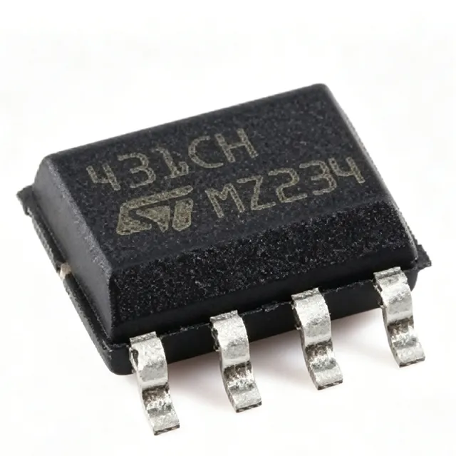
TL431CDT - Adjustable Precision Shunt Regulator | STMicroelectronics
The STMicroelectronics TL431CDT is a three-terminal adjustable precision shunt regulator with a guaranteed reference voltage tolerance of 2.495 V ±1% over the full operating temperature range. It is offered in the industry-standard SOT-23-3 package, making it a compact and cost-effective solution for voltage regulation, error amplification, and reference voltage generation in a wide variety of applications. Data verified as of 2026-08-05. A shunt regulator is a type of voltage regulator that maintains a stable output voltage by shunting excess current to ground through a variable impedance path. The TL431 is a programmable precision reference that can be configured as a shunt regulator, series regulator, or error amplifier by adding external resistors. It belongs to the family of adjustable precision references, which are fundamental building blocks in power management and analog circuits, sitting between discrete Zener diodes and more complex integrated regulators. Key features of the TL431CDT include a reference voltage of 2.495 V with ±1% accuracy, a cathode voltage range of 2.5 V to 36 V, and a cathode current range of 1 mA to 100 mA. The device offers a typical dynamic output impedance of 0.2 Ω, ensuring excellent load regulation. It also features a low output noise of 90 nV/√Hz and a fast turn-on response, making it suitable for high-frequency applications. The TL431CDT is built using a bipolar process technology, providing stable performance over a wide temperature range of -40°C to +105°C. The SOT-23-3 package is lead-free and RoHS compliant, with a compact footprint of 2.9 mm × 1.6 mm, ideal for space-constrained designs. The device is also available in other package options, but the CDT suffix specifically denotes the SOT-23-3 package with tape and reel packaging. Typical applications include precision voltage references for power supplies, error amplifiers in switching power supplies, voltage monitoring circuits, and adjustable output voltage regulators. The TL431CDT is also widely used in battery chargers, LED drivers, and automotive electronics where accurate voltage regulation is critical. When designing with the TL431CDT, ensure that the cathode current is maintained within the specified range (1 mA to 100 mA) to guarantee proper regulation. The device requires a minimum cathode current of 1 mA to operate correctly, and an external resistor is needed to set the bias current. For optimal stability, place a bypass capacitor at the cathode to ground, especially in high-frequency applications. This page synthesizes distributor pricing, drop-in alternatives, and practical design notes not found in the STMicroelectronics datasheet, providing engineers with a comprehensive resource for selecting and implementing the TL431CDT.
TL431IDBZR - Adjustable Shunt Voltage Reference 36V SOT-23-3 | TI
The Texas Instruments TL431IDBZR is a three-terminal adjustable precision shunt voltage reference with a 2.495V reference voltage, 36V maximum cathode voltage, and 100mA cathode current capability, housed in a 3-pin SOT-23-3 (DBZ) package with I-grade accuracy of ±2.2% over the -40C to +85C industrial temperature range. A shunt voltage reference is a type of voltage regulator that operates by sinking or sourcing current through itself to hold a fixed voltage across its terminals, working in parallel with the load rather than in series. Within the power management hierarchy, it sits alongside series references and bandgap references as a foundational voltage-reference IC. The TL431 family is the industry-defining shunt regulator: two external resistors program any output voltage from Vref (2.495V) up to 36V, effectively acting as a programmable Zener diode with far tighter tolerance and much sharper knee. Key features of the TL431IDBZR include the 2.495V reference (with B, A, and standard grades offering 0.5%, 1%, and 2% initial tolerance respectively), a low dynamic output impedance, fast response, and operation across the full industrial -40C to +85C range with approximately 109 ppm/C temperature coefficient according to third-party datasheet compilations. Technically, the TL431 integrates an internal 2.495V bandgap reference feeding the inverting input of an internal operational amplifier whose output drives an output transistor. When the REF pin exceeds 2.495V, the cathode conducts and regulates. This closed-loop behavior yields excellent line and load regulation and makes the part usable as a comparator with a built-in reference in feedback loops. Typical applications include the feedback error amplifier in isolated flyback and forward SMPS designs (paired with an optocoupler), adjustable Zener clamps in battery chargers, voltage monitoring and supervisory circuits, and precision current-source biasing. Its 100mA sink capability directly drives optocoupler LEDs. Design tip: always provide a minimum cathode current (typically around 1mA) to guarantee regulation, and add a small compensation network around the REF pin to stabilize feedback loops, since the TL431's output impedance interacts with loop capacitance. This page adds value beyond the manufacturer datasheet by consolidating verified distributor data, drop-in alternatives across TI and cross-brand sources, parameter comparisons, and practical design notes in one place.
TL431QDBZR - 36V Adjustable Shunt Voltage Reference | TI
The Texas Instruments TL431QDBZR is an adjustable precision shunt voltage reference with a 2.495V reference voltage, output tolerance of ±2.2%, and cathode current capability up to 100 mA, housed in a 3-pin SOT-23 (DBZ, TO-236AB) surface-mount package. A shunt voltage reference is a type of voltage reference IC that regulates voltage by shunting (bypassing) excess current to ground through an internal transistor, placed in parallel with the load. Within the power management hierarchy, it sits under voltage references alongside series references, and is widely used as an error amplifier and feedback element in isolated and non-isolated power supplies. Key features include a programmable output voltage set from Vref (2.495V) up to the 36V maximum cathode voltage using just two external resistors, a low dynamic output impedance of approximately 0.22 ohm (typical), a sharp low-current turn-on characteristic, and operation across the -40C to +125C automotive-relevant Q temperature grade. The TL431 integrates a 2.495V bandgap reference and an internal output driver, effectively functioning as a single-supply error amplifier with an open-collector-style cathode output. This architecture allows it to compare a divided-down feedback voltage against its internal reference and directly drive an optocoupler LED in isolated flyback converters, eliminating a separate op-amp. Typical applications include adjustable shunt regulation in AC-DC adapters, secondary-side feedback regulation in isolated flyback and forward SMPS designs, overvoltage protection crowbar circuits, and setpoint control in LED drivers and battery chargers. A key design consideration: the device requires a minimum cathode current of roughly 1 mA to maintain regulation, so the resistive divider and bias network must guarantee this minimum under worst-case load conditions. This page synthesizes distributor pricing, verified drop-in alternatives across multiple manufacturers, and practical design notes not found in the manufacturer datasheet.
TL432AIL3T - 2.495-36V Adj Shunt V-Ref, 1%, SOT-23-3 | STMicroelectronics
The STMicroelectronics TL432AIL3T is an adjustable shunt voltage reference in a 3-pin SOT-23-3 (L3T) surface-mount package, offering a programmable output of 2.495 V to 36 V with 1% voltage tolerance and 100 mA cathode current capability. It features a typical output impedance of 0.22 ohm and operates across an automotive-grade temperature range of -40 C to +125 C. A shunt voltage reference is a two-terminal device that behaves like a programmable Zener diode: when biased with a current source above its minimum cathode current (typically 1 mA), it holds its cathode voltage at a precise reference value. The TL432 extends the classic TL431 family with a reverse pinout (cathode-anode-reference on pins 1-2-3 instead of reference-anode-cathode), enabling simpler PCB routing in many polarity-sensitive designs. The TL432 belongs to the broader class of linear voltage references - subcategory of power management ICs - sitting alongside series and shunt regulators. Key features include guaranteed temperature stability across the full automotive range, 100 mA continuous sink current capability, low typical output impedance of 0.22 ohm, and a sharp turn-on characteristic that makes it usable as a voltage comparator or error amplifier. The 1% voltage precision grade (A suffix) suits precision analog circuits, while the lower-cost B and C grades offer 1% and 2% tolerance for cost-optimized designs. The TL432 uses a buried-Zener bandgap architecture with on-chip temperature compensation. Output voltage is programmed by an external resistor divider: VOUT = VREF * (1 + R1/R2), where VREF = 2.495 V. The same die is offered in the TL431 family with mirrored pinout, allowing engineers to standardize on one footprint design. Typical applications include adjustable voltage regulators, switching power supply feedback loops, precision current sources, ADC/DAC reference rails, and automotive ECU voltage monitoring. The wide 2.495 V to 36 V output range and automotive temperature grade make it suitable for 12 V/24 V automotive subsystems and industrial 24 V bus systems. When designing with the TL432, always ensure cathode current stays between 1 mA (minimum) and 100 mA (maximum), and add a 0.1 uF bypass capacitor across the reference node when used in noisy switching environments. The SOT-23-3 package has a thermal resistance around 250 C/W, so continuous dissipation above 50 mW requires thermal analysis. This page synthesizes distributor pricing, drop-in alternatives, and practical design notes not found in the manufacturer datasheet alone.
TL432BSA-7 - Adjustable Shunt Reference, 36V, ±0.5%, SOT-23-3 | Diodes Incorporated
The Diodes Incorporated TL432BSA-7 is a three-terminal adjustable precision shunt regulator housed in a compact SOT-23-3 surface-mount package. It provides an adjustable output voltage from 2.495V to 36V with ±0.5% initial accuracy and supports cathode currents up to 100 mA, making it a versatile building block for precision reference and error-amplifier applications. A shunt voltage reference is a two-terminal device that maintains a fixed voltage across its cathode-anode terminals by sinking current to ground, analogous to a Zener diode but with much tighter tolerance, lower dynamic impedance, and better temperature stability. The TL432 family (and the related TL431 family) belongs to the broader category of programmable shunt regulators, which are key analog building blocks in power management, signal conditioning, and feedback loops. They occupy the same hierarchical role as bandgap voltage references, Zener references, and series voltage regulators, but differ by being driven by current rather than input voltage. Key features of the TL432BSA-7 include an adjustable reference voltage set by an external resistor divider, low dynamic output impedance across the operating current range, and a wide cathode operating current window from 1 mA to 100 mA. The TL432 pinout reverses the reference (REF) and anode (A) positions relative to the TL431, so it is NOT a drop-in pin replacement for TL431 footprints. The reference tolerance is graded by suffix: 'B' designates ±0.5%, 'A' designates ±1.0%, and standard is ±2.0%. The TL432BSA-7 uses a bandgap core stabilized by on-chip temperature-compensation circuitry to deliver a flat temperature coefficient across the full industrial -40 °C to +125 °C range. The low dynamic impedance (~0.5 ohm typical) and 100 mA cathode capability allow it to serve as both a precision reference and a feedback error amplifier in isolated and non-isolated switching power supply topologies. Typical applications include switching power supply feedback loops, precision constant-current sinks, adjustable voltage references in industrial control, ADC/DAC reference rails, battery chargers, and comparator-style overvoltage monitors. Its SOT-23-3 footprint also suits high-density analog boards where a TL431 TO-92 part would be too large. When designing with the TL432BSA-7, verify the pinout against the TL431 footprint on existing PCBs, since the REF and ANODE pins swap positions. Provide at least 1 mA of cathode bias current to keep the device in regulation, and bypass the reference pin with a 0.1 µF capacitor when noise-sensitive ADCs are tied to the reference ladder. This page synthesizes distributor pricing, drop-in alternatives sourced from the TL432 and TL431 pin-compatible families, and practical design notes not found in the manufacturer datasheet alone.
TL432LIBQDBZR - Adjustable 2.495V Shunt Reference, ±0.5% | TI
The Texas Instruments TL432LIBQDBZR is an adjustable precision shunt voltage reference featuring a 2.495V nominal reference and an input range of 2.495V to 36V in a SOT-23-3 (DBZ) package. It delivers ±0.5% initial cathode tolerance (B grade) at 25°C, a 15 mA maximum cathode current, and a 400 nA minimum cathode current, with optimized reference and deviation currents that improve system accuracy versus legacy TL431 designs. A shunt voltage reference is a two-terminal (or three-terminal with adjust) device that behaves like a non-inverting precision Zener diode. When biased with a resistor from a higher supply, it holds its cathode-to-anode voltage fixed at the programmed VREF, allowing any desired reference voltage to be set with external resistors. The TL432LI sits within the hierarchical group: shunt reference -> voltage reference -> power management IC -> analog semiconductor. It is functionally equivalent to the TL431 family but offers a different pinout in the SOT-23-3 package and improved IREF/Idev characteristics. Key features include adjustable cathode voltage from 2.495V up to 36V, a typical output impedance of 0.2 ohm, low cathode current of 400 nA min and 15 mA max, and operation across the automotive -40°C to +125°C range. The SOT-23-3 (DBZ) outline is footprint-compatible with the standard TL431/TL432 family, easing second-source sourcing. The TL432LI is also offered in 1% (A) tolerance grades for tighter designs. Technologically, the TL432LI uses a buried-Zener bandgap core with trimmed thin-film resistors to achieve tight initial tolerance and low temperature drift. The optimized IREF/Idev values minimize the error terms introduced by the feedback divider at low cathode currents, enabling high-accuracy closed-loop designs without the bias-induced errors seen in classic TL431 circuits. Typical applications include adjustable linear regulator feedback, switching-mode power supply (SMPS) error-amplifier reference, isolated point-of-load rails, automotive voltage monitors, and ADC/DAC precision references. The wide cathode operating range also makes it useful in high-voltage rails up to 36V. When designing with this part, remember the TL432LI pinout in the SOT-23-3 differs from the TL431 in the same package - pin 1 is REF, pin 2 is ANODE, and pin 3 is CATHODE. Verify orientation against the datasheet footprint before PCB reuse. This page synthesizes distributor pricing, drop-in alternatives, and practical design notes not offered as a single view on the manufacturer datasheet, helping engineers compare sourcing options and pinout compatibility at a glance.
TL432LIBQDBZRQ1 - Adjustable Shunt Reference, 0.5% | TI
The Texas Instruments TL432LIBQDBZRQ1 is an automotive-grade adjustable shunt voltage reference IC with 2.495 V nominal reference and adjustable output up to 36 V, packaged in a 3-pin SOT-23 (DBZ) with ±0.5% initial tolerance (B grade) and 15 mA cathode current capability. Per the manufacturer datasheet, the device belongs to the TL431LI-Q1/TL432LI-Q1 family with optimized reference current for lower minimum operating current and tighter thermal stability. A shunt voltage reference (also called a programmable zener reference) is a two-terminal or three-terminal device that maintains a fixed voltage at its cathode when biased with sufficient current. The three-terminal form adds a reference pin, allowing the cathode voltage to be programmed above the internal reference using an external resistor divider. The TL432 sits within the broader hierarchy of voltage references -> shunt regulators -> analog ICs -> power management semiconductors, and is commonly used in closed-loop feedback for switching power supplies, where it sets the output voltage set point. Compared to two-terminal zener diodes, three-terminal shunt references offer tighter initial tolerance, lower dynamic impedance, and programmability. Key features include an adjustable output voltage range from 2.495 V (VREF) to 36 V set by two external resistors, a typical output impedance of 0.2 Ω that minimizes set-point shift with cathode current, and an optimized reference current designed for low minimum cathode current (I_min) operation. The device is specified across the automotive temperature range, qualified to AEC-Q100 standards, and supports solder reflow up to 260 °C per JEDEC J-STD-020. Internally, the TL432 uses a bandgap reference core with on-chip op-amp drive to a pass transistor, providing stable VREF across temperature, supply, and load variations. The TL432 pinout is the reverse-polarity variant of the TL431: in the DBZ (SOT-23-3) package, the TL432 places the reference (REF) on pin 1, anode on pin 2, and cathode on pin 3, while the TL431 has anode on pin 1, cathode on pin 2, and reference on pin 3. Always verify pinout before substituting between TL431 and TL432. Typical applications include isolated flyback converter secondary-side regulation, primary-side regulation with optocoupler feedback, automotive battery monitoring, precision current limiting, and adjustable zener replacement. The TL432LI-Q1 variants (LI suffix) provide optimized reference current for lower I_min and tighter TI operation versus the standard TL431/TL432 parts. When designing with this device, ensure cathode current stays within the datasheet limits (typically 1 mA minimum, 15 mA continuous) across all load and temperature conditions. Add a 0.1 µF bypass capacitor at the reference pin if the divider impedance is high to prevent oscillation. This page synthesizes distributor pricing, AEC-Q100-qualified drop-in alternatives, and practical design notes not found in the manufacturer datasheet alone.
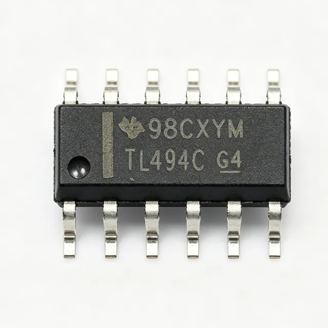
TL494CDT - PWM Controller IC | STMicroelectronics | SMPS
The TL494CDT is a fixed-frequency pulse-width modulation (PWM) control circuit from STMicroelectronics, designed primarily for switch-mode power supplies (SMPS). It integrates all the functions required for a single-ended or push-pull switching power supply, including an internal oscillator, error amplifiers, a 5V reference, and output control logic. The device operates from a supply voltage of 7V to 40V and is available in a 16-pin SOIC (SOP-16) package, making it suitable for compact power supply designs. A PWM controller is a specialized integrated circuit that generates a variable-duty-cycle square wave to regulate the output voltage of a switching power supply. It compares a feedback signal to a reference voltage and adjusts the duty cycle of the output transistors accordingly. The TL494 belongs to the family of voltage-mode PWM controllers, which are widely used in offline and DC-DC converters due to their simplicity and robustness. This category sits within the broader hierarchy of power management ICs, which also includes linear regulators, switching regulators, and battery management devices. Key features of the TL494CDT include a complete PWM power-control circuitry, an uncommitted output for single-ended or push-pull operation, an internal oscillator with a frequency range of 1kHz to 300kHz, and a 5V reference with 5% tolerance. It also provides an error amplifier with a common-mode voltage range of -0.3V to VCC-2V, a dead-time control comparator, and a standby current of typically 6mA. These features enable precise regulation and protection in various power conversion topologies. The TL494CDT uses a bipolar process technology, offering a proven and reliable architecture that has been in production for decades. It includes an internal 5V reference that can source up to 10mA for external use, and its output stage can sink or source up to 250mA. The device also features a shutdown control pin that can be used for overcurrent or overvoltage protection, and its dead-time control allows adjustment of the minimum off-time to prevent transformer saturation in push-pull designs. Typical applications include switch-mode power supplies for computers, telecom equipment, industrial systems, and battery chargers. The TL494CDT is also used in DC-DC converters, inverters, and motor control circuits. Its wide supply voltage range and flexible output configuration make it a versatile choice for both single-ended and push-pull topologies. When designing with the TL494CDT, it is important to properly set the oscillator frequency using external timing components (RT and CT) and to ensure adequate decoupling of the VCC pin. The dead-time control pin should be used to prevent shoot-through in push-pull stages, and the error amplifier compensation network must be designed for stable loop operation. This page synthesizes distributor pricing, drop-in alternatives, and practical design notes not found in the STMicroelectronics datasheet, providing a comprehensive resource for engineers selecting a PWM controller for their power supply design.

TL594INSR - 40V 0.2A 300kHz PWM Controller | Texas Instruments
The Texas Instruments TL594INSR is a 40 V, 0.2 A, 300 kHz pulse-width-modulation (PWM) controller with integrated undervoltage lockout (UVLO), housed in a 16-pin Small-Outline (SOP/NS) package supplied on tape and reel. The device integrates a precision reference, two error amplifiers, an adjustable oscillator, a dead-time control comparator, and uncommitted output transistors capable of sinking or sourcing up to 200 mA each for driving power stages directly. What is a PWM controller? A PWM controller is a power-management integrated circuit that generates switching signals whose duty cycle is modulated to regulate voltage or current in switching power supplies. The TL594 belongs to the voltage-mode PWM controller category, which sits in the hierarchy of PWM controller -> switching controller -> DC-DC controller -> power management IC -> semiconductor. Voltage-mode controllers regulate by comparing an error-amplifier output to a sawtooth waveform, making them robust, well-understood, and tolerant of noisy measurement environments. The TL594INSR supports buck, boost, flyback, forward, full-bridge, half-bridge, and push-pull topologies, giving designers a single IC for multiple converter architectures. Key features include 5 V (±5%) internal reference output, programmable dead-time control (DTC), programmable oscillator frequency up to 300 kHz via external RT and CT, and uncommitted 200 mA open-collector outputs that can be configured in common-emitter or emitter-follower mode for either single-ended or push-pull operation. At the architecture level, the TL594 uses a bandgap-derived 5 V reference feeding two identical error amplifiers with uncommitted inputs and outputs, allowing flexible feedback loop design. The oscillator section generates a sawtooth whose rise time is set by RT-CT and whose maximum frequency is 300 kHz, with internal circuitry that prevents simultaneous conduction of the output stages during transitions (dead-time control). Protection features include UVLO with typical 6 V turn-on threshold and thermal considerations for the SOP-16 (NS) thermal pad. Typical applications include DC-DC converters in industrial power systems, SMPS for telecom and networking equipment, battery chargers using buck or boost topologies, and motor-drive forward converters. Designers favor the TL594 for its topology flexibility and proven architecture in long-lifecycle designs. When designing with this part, ensure RT and CT values are selected to keep oscillator frequency below 300 kHz under all temperature and tolerance conditions, and add adequate bulk capacitance on VCC to prevent UVLO retriggering during start-up.

TL750M05CKCSE3 - 750mA 5V LDO Regulator, TO-220 | Texas Instruments
The Texas Instruments TL750M05CKCSE3 is a 750-mA, 5V fixed-output, low-dropout positive voltage regulator housed in a 3-pin TO-220 (KCS) package with tab. Designed specifically for battery-powered and automotive systems, it delivers a regulated 5V output at up to 750 mA from a wide input range up to 26 V, with very low dropout voltage and extremely low quiescent current. The device is fully protected against 60-V load-dump transients, reverse-battery conditions, overvoltage, and includes internal thermal-overload and overcurrent-limiting protection. What is an LDO (Low-Dropout) linear regulator? An LDO is a type of linear voltage regulator that maintains a stable output voltage even when the input voltage is only slightly higher than the output - the 'dropout' voltage. Compared to standard regulators, LDOs offer tighter regulation, faster transient response, and very low quiescent current, making them ideal for post-regulation after a switching converter or for direct battery-powered applications. In the broader taxonomy, the TL750M05 belongs to linear regulators, a subset of voltage regulators, which sit under power management ICs in the semiconductor hierarchy. Key features include very low dropout voltage (less than 750 mV at full load), 60-V load-dump protection, internal current limiting, thermal shutdown, and reverse-battery protection. The fixed 5V output eliminates external resistor dividers, simplifying the BOM. The TO-220 package with metal tab enables direct PCB mounting or heatsink attachment for high-power dissipation. The TL750M05CKCSE3 uses a bipolar pass-element architecture optimized for very low quiescent current draw, which extends battery life in standby conditions. It is specifically engineered to survive the harsh electrical environment of automotive 12V systems, including jump-start, load-dump, and reverse-battery events. Typical applications include automotive infotainment and instrument clusters, body control modules, post-regulation after switching converters, battery-powered industrial equipment, and any 12V/24V system that requires a regulated 5V rail with robust transient protection. The TL751M series variant adds an enable pin for power sequencing. When designing with this device, ensure input and output capacitors are placed close to the IC, and use a sufficient copper pour or external heatsink when VIN-VOUT differential is high. The tab is electrically connected to ground or output depending on the version - always verify against the datasheet before mounting. This page synthesizes distributor pricing, drop-in alternatives from the same TL750M family, and practical design notes not found in the manufacturer datasheet alone.

TLC5947DAPR - 24-Ch 12-Bit PWM LED Driver | Texas Instruments
The Texas Instruments TLC5947DAPR is a 24-channel, 12-bit constant-current sink LED driver with an internal oscillator, housed in a 32-pin HTSSOP (DAP) package with PowerPAD. Each of the 24 channels is individually adjustable with 4096 PWM grayscale steps, and the current of all 24 outputs is set by a single external resistor. Per-channel output current is rated at 30 mA. What is a constant-current LED driver? A constant-current LED driver is a specialized power management IC that regulates the current flowing through each LED string to a precise setpoint, regardless of variations in forward voltage, temperature, or supply voltage. Compared to a simple current-limiting resistor, it improves brightness uniformity, extends LED lifetime, and enables per-channel grayscale dimming. Constant-current sinks sit hierarchically inside LED drivers, which themselves are a sub-category of power management ICs alongside voltage regulators and battery management devices. The TLC5947DAPR further extends this role by adding 12-bit PWM grayscale control, dimming that circuit apart from any discrete MOSFET dimmer or boost-converter driver. Key differentiating features include 30 mA per-channel constant-current sinking, 12-bit (4096-step) PWM grayscale resolution, an internal oscillator that removes the need for an external PWM clock, a serial shift-register interface for cascaded multi-device chains, and integrated thermal shutdown. The wide VCC supply range supports battery and bus-powered designs, while 24 channels per IC minimize driver count in large LED matrices and signage. Architecturally, the TLC5947DAPR uses a serial-in/parallel-out shift register feeding 24 internal PWM counters that are clocked by the internal oscillator. Gray scale (GS) data is latched into the device via the serial interface and automatically replayed each PWM cycle, freeing the host microcontroller from continuous refresh. A single external IREF resistor sets the global current for all 24 channels, simplifying BOM while preserving per-pixel dimming accuracy. Typical applications include full-color LED video displays, RGB signage, architectural lighting, decorative and stage lighting, and large LED matrix backlighting. The cascading serial interface also makes it well suited to daisy-chained WS2812x-style "NeoPixel" replacement designs where deterministic, hardware-refreshed grayscale is required without MCU overhead. When designing with this device, place the IREF resistor close to the IREF pin to minimize noise pickup, and ensure the PowerPAD is soldered to a sufficient copper area (typically 1 square inch) to keep junction temperature within the 150 C thermal-shutdown limit under full 24-channel load. This page synthesizes distributor pricing, drop-in alternatives, and practical design notes not found in the manufacturer datasheet alone.

TLC5955RTQR - 48-Ch 16-Bit PWM LED Driver w/ DC, BC | TI
The Texas Instruments TLC5955RTQR is a 48-channel, constant-current sink LED driver with 16-bit (65,536-step) PWM grayscale control, 7-bit (128-step) dot correction, and 8-bit brightness control, housed in a 56-pin QFN (RTQ) 8x8 mm package. It supports per-channel sink current up to 23.9 mA when VCC ≤ 3.6 V (MC = 5) and 31.9 mA when VCC > 3.6 V (MC = 7), with on-chip open/short LED detection. An LED driver is a specialized power-management IC that translates low-voltage digital brightness data into precisely regulated constant currents, allowing each LED in a matrix to be set to an exact luminance level. The TLC5955 belongs to the constant-current LED driver sub-category within Power Management ICs, sitting between generic GPIO expanders and high-voltage LED matrix drivers. It is typically used in displays where uniform brightness and fine grayscale steps matter more than raw current capability. Key features include 48 individually-controllable constant-current sink outputs, 16-bit Enhanced Spectrum or Conventional PWM grayscale, 7-bit dot correction that compensates brightness mismatch between LED channels, 8-bit global brightness control, on-chip circuitry that detects open or shorted LEDs failures in real time, an internal current setting register eliminating many external resistors, and a 30 MHz cascadable serial interface. The serial shift register design lets multiple TLC5955s share one SPI/QSPI bus for very large panels. Internally, the device uses a precision bandgap reference and matched current-mirror sinks. A global 8-bit brightness register scales all 48 channels simultaneously for overall panel brightness, while the 7-bit DC register fine-tunes each channel's bias current to mask LED forward-voltage variation. The 16-bit PWM counter is clocked from an external GS reference clock, and Enhanced Spectrum PWM spreads the switching edges across multiple sub-frames to reduce EMI peak energy. Open/short detection compares each output voltage against programmable thresholds between successive PWM refresh cycles without disturbing the panel image. Typical applications include full-color RGB LED video displays, indoor/outdoor LED signs, LED billboard panels, decorative architectural lighting, and stage lighting fixtures. The TLC5955 is especially well suited to high-channel-count panels where a single MCU cannot provide enough PWM pins and where uniform brightness across thousands of LEDs is critical. When designing with this part, route the GSCLK and SCLK lines as controlled-impedance traces and keep them away from the constant-current outputs to avoid coupling. Place the 0.1 µF VCC decoupling capacitor within 3 mm of the supply pin and follow the datasheet ground-plane recommendations. Note that VCC must be in the 3 V to 5.5 V range while the LED supply (VLED) can be higher, and the sink outputs can withstand up to 17 V per channel. This page consolidates distributor pricing, true drop-in alternatives, and practical design notes that go beyond the bare datasheet, giving an engineer a single reference for selecting and sourcing the TLC5955RTQR.

TLC6C5712QPWPRQ1 - 12-Ch AEC-Q100 LED Driver | Texas Instruments
The Texas Instruments TLC6C5712QPWPRQ1 is an automotive-grade 12-channel constant-current-sink LED driver with full diagnostics and PWM dimming, delivering up to 75 mA per channel from a 3 V to 5.5 V supply in a 28-pin HTSSOP (PWP) package. Per the TI product page, the device is qualified to AEC-Q100 for -40C to +125C operation. A constant-current-sink LED driver is a type of linear LED driver IC that regulates the current flowing through each LED string by sinking a precisely controlled current to ground. Within the power-management hierarchy, it sits under LED drivers -> linear current regulators -> power management ICs. Unlike simple resistive ballast or open-drain switches, a constant-current sink holds LED brightness constant despite forward-voltage variation, supply drift, and temperature change, which is essential for color and brightness consistency. Key features include 12 independent current-sink outputs rated at 75 mA each, PWM-based dimming for precise brightness control, and a comprehensive diagnostic suite that detects open-circuit, short-circuit, and other fault scenarios. TI designed this device specifically for safety-critical automotive cluster lighting, where system-level functional-safety considerations demand per-channel fault detection to maintain brightness and color-temperature consistency across many LEDs. Technically, the device uses a 12-bit architecture with internal current-setting registers and serial control, allowing the microcontroller to program per-channel current and read back diagnostic status. The current-sink topology is linear, adding no switching noise to the LED rails, while PWM dimming achieves wide-range average brightness without color shift. Output voltage rating of 7 V provides headroom for LED stack variation. Typical applications include automotive instrument-cluster backlighting, indicator and telltale LEDs, and other safety-critical multi-channel LED lighting in vehicles. The 12-channel density reduces BOM count versus discrete transistor solutions while adding diagnostics unavailable in discrete designs. A key design consideration is thermal dissipation: at 75 mA per channel with a large LED-headroom voltage, package power dissipation must be checked against the HTSSOP PowerPAD thermal capability, using copper pour under the pad. This page adds value beyond the datasheet by synthesizing distributor pricing, availability, drop-in alternative analysis, and practical design notes in one place.
TLC6C5724QPWPRQ1 - 24-Channel 50mA LED Driver, AEC-Q100 | TI
The Texas Instruments TLC6C5724QPWPRQ1 is an automotive-grade 24-channel constant-current RGB LED driver with full LED diagnostics, delivering up to 50 mA per output channel in a 38-pin HTSSOP (PWP) package with exposed pad. It features 7-bit dot correction with two ranges per output, 8-bit group intensity control per color group, and 12-, 10-, or 8-bit PWM dimming resolution. A constant-current LED driver is a type of power management IC that regulates current (rather than voltage) through LED strings. Because LED brightness and color depend directly on forward current, constant-current drivers eliminate the brightness variation that plagues simple resistive ballast designs. Within the power management hierarchy, the TLC6C5724-Q1 belongs to the linear LED driver family with integrated PWM dimming and dot correction, positioned as a system-level solution for matrix and string LED lighting control. Key differentiating features include the per-channel 7-bit dot correction with two selectable current ranges, which lets a single design compensate for LED forward-voltage binning across red, green, and blue dies; group-level 8-bit intensity control that simplifies color calibration; and a selectable 12-bit PWM engine supporting dimming ratios suited to automotive interior and exterior lighting. The full-diagnostics subsystem detects open-circuit and short-circuit LED faults, output shorts to GND, and provides fault reporting for functional-safety-oriented designs. Architecturally, the TLC6C5724-Q1 combines a constant-current sink per channel with an external resistor that sets the full-scale 50 mA maximum output current, a serial data interface for configuration, and an on-chip diagnostic engine that scans LED health during operation. Grayscale and dot-correction data are latched internally, allowing PWM dimming to continue glitch-free while new data shifts in, an important behavior for seamless brightness transitions. Typical applications include automotive RGB ambient interior lighting, rear combination lamps and turn indicators, architectural and accent lighting, and RGB status or backlighting in industrial displays. Its AEC-Q100 qualification and full diagnostics make it especially suitable for safety-relevant exterior lighting where fault reporting is required. When designing, set the external current-setting resistor so the 50 mA absolute maximum per-channel current is respected across temperature, and budget thermal dissipation for the worst-case channel currents in the exposed-pad HTSSOP package with an adequate copper pour. This page synthesizes verified distributor data, drop-in same-family alternatives, AEO-optimized FAQs, and practical design notes not found in the manufacturer datasheet.
TLD11141EPXUMA1 - 180mA 40V LITIX Basic+ LED Driver | Infineon
The Infineon TLD11141EPXUMA1 is a single-channel high-side LED driver IC from the LITIX Basic+ family, delivering up to 180 mA of regulated constant current to a high-side connected LED load from a 40 V supply rail, housed in a 14-pin PG-TSDSO-14 surface-mount package with exposed thermal pad. It integrates an output stage and a single-channel driver, supporting both DC operation and PWM dimming for accurate brightness control across automotive and industrial lighting. Background Knowledge: An LED driver IC is a specialized constant-current source that regulates the current through a high-brightness LED (HB-LED), protecting it from supply transients and thermal runaway while enabling brightness control. The category hierarchy is: LED driver -> lighting driver -> power management IC -> semiconductor. High-side drivers, like the TLD1114-1EP, place the current source between the supply rail and the LED anode, leaving the LED cathode at ground, which simplifies wiring in chassis-grounded systems and avoids ground-shift issues. This makes them ideal for automotive body and tail-light applications where one terminal is chassis-referenced. The TLD11141EPXUMA1 delivers up to 180 mA per channel, supports a wide 5.5 V to 40 V supply range (load-dump tolerant), and provides PWM dimming capability for variable brightness. Its integrated output stage minimizes external component count, while built-in protection features include over-temperature shutdown, short-circuit protection, and reverse-polarity robustness typical of Infineon's LITIX Basic+ family. The PG-TSDSO-14 exposed-pad package provides low thermal resistance, allowing reliable operation at the device's rated current. Internally, the device uses a precision bandgap reference and a current-sense architecture that regulates output current independent of LED forward voltage variations across temperature. The high-side drive topology simplifies PCB routing and supports parallel-channel configurations via multiple TLD1114-1EP devices for higher-current LED strings or multi-channel lighting systems. Typical applications include automotive tail lights, brake lights, daytime running lights (DRL), interior ambient lighting, status indicators, and industrial signage. The PWM dimming interface allows direct connection to a microcontroller for dynamic brightness adjustment, supporting safety features such as dynamic turn signals. When designing with this device, observe the maximum junction temperature rating and use adequate PCB copper area on the exposed pad to maintain thermal performance. Always verify the output current setting resistor value against the LED manufacturer's recommended forward current, and add an input capacitor close to the supply pin for load-dump and EMI robustness. This page synthesizes distributor stock data, drop-in alternative MPNs from the LITIX Basic+ family, and practical thermal/design guidance that goes beyond the manufacturer datasheet excerpts.

TLD1124ELXUMA1 - 360mA 1-Ch Linear LED Driver | Infineon LITIX
The Infineon TLD1124ELXUMA1 is a one-channel high-side linear LED driver IC from the LITIX™ Basic family, delivering up to 360 mA continuous output current to drive high-power LEDs in automotive lighting systems. Housed in a 14-pin PG-SSOP-14-EP (exposed pad) package, it integrates the output stage, current sense, and protection circuitry to provide a compact, robust solution for constant-current LED strings fed from a 5 V to 40 V supply rail. A linear LED driver (also called an LED controller or linear current regulator) is a power-management IC that maintains a constant, programmed current through an LED or LED string rather than a constant voltage. Within the broader power hierarchy, linear LED drivers sit beneath switching DC-DC LED drivers and above simple ballast resistors; they trade conversion efficiency for ultra-low EMI, fast PWM dimming response, and minimal external component count — making them the preferred topology for noise-sensitive or cost-sensitive automotive lamp modules. Key features of the TLD1124ELXUMA1 include an adjustable constant output current up to 360 mA set by a single external sense resistor, a wide supply range suited to automotive 12 V and 24 V bus systems, integrated PWM dimming via an enable/dimming input, and comprehensive protection including open-LED, short-to-GND, short-to-battery, over-temperature, and over-current diagnostics. The exposed thermal pad of the PG-SSOP-14-EP package provides a low θJA path to the PCB copper, which is essential when dissipating several watts in a linear topology. The device is qualified to AEC-Q100 for automotive use and is targeted at rear lamps, daytime running lights, interior mood lighting, and instrument-panel backlighting. Typical design tips: choose a sense resistor of roughly 0.5 Ω to 1.5 Ω to program the 360 mA nominal current, keep the input bypass capacitor within 5 mm of the VS pin, and connect the exposed pad to a copper area of at least 1 cm². This page synthesizes distributor pricing, drop-in alternatives, and practical design notes not found in the manufacturer datasheet alone.
TLD1125ELXUMA1 - 1-Ch 360mA Linear LED Driver | Infineon LITIX
The Infineon TLD1125ELXUMA1 is a one-channel high-side constant-current LED driver IC from the LITIX Basic family, delivering up to 360 mA of regulated output current in a 14-pin PG-SSOP-14-EP package with exposed thermal pad. It is designed for linear driving of low- to medium-power LEDs in automotive and industrial lighting applications, with PWM dimming support for brightness control. What is a linear LED driver? A linear LED driver is a semiconductor device that regulates the current flowing through an LED string by dissipating excess voltage as heat across an internal pass element, instead of switching the inductor as a DC-DC converter does. Linear LED drivers sit within the broader power-management IC hierarchy: linear LED driver -> constant-current driver -> LED driver -> power management IC -> semiconductor. They are valued for low EMI, no inductor requirement, and very small PCB footprint, at the cost of reduced electrical efficiency compared to switching topologies. The TLD1125EL integrates an output stage that sustains load currents up to 360 mA, supports PWM dimming for precise brightness modulation, and includes protection features such as over-temperature shutdown, open-LED detection, and short-to-ground protection. Its 14-pin SSOP with exposed pad enables efficient heat removal on the PCB copper, which is essential because the linear topology converts the VIN-VLED drop into thermal energy. Automotive qualification per AEC-Q100 makes it directly suitable for tail lamps, daytime running lights (DRL), turn indicators, and interior ambient lighting. The output stage architecture combines a reference, error amplifier, and power transistor monolithically, achieving tight output-current accuracy and stable behavior across temperature. The exposed thermal pad (EP) on the bottom of the package provides a low thermal-resistance path to the PCB copper, enabling sustained high-current operation without external heatsinking. Typical applications include automotive rear combination lamps, turn signal indicators, daytime running lights, interior ambient lighting, and industrial signage or status indicators. Its footprint compatibility with other Infineon LITIX Basic family members allows platform reuse across lighting variants with different current ratings. When designing with this part, size the PCB copper pour beneath the exposed pad to keep the junction temperature below 150 C, and ensure that VIN does not exceed the absolute maximum rating even during load-dump transients. Place the decoupling capacitor close to the supply pin to stabilize the internal reference. This page synthesizes distributor pricing, pin-to-pin compatible alternatives, and practical design notes that supplement the manufacturer datasheet for faster engineering decisions.

TLD11731ETXUMA1 - 400mA Linear LED Driver | Infineon LITIX
The Infineon TLD11731ETXUMA1 is a single-channel low-side LED driver IC with 400 mA output current, packaged in a 16-pin PG-TFDSO-16-1 (TSSOP-16 exposed pad) surface-mount package. The device integrates a 1-channel linear current sink with PWM dimming support and Infineon's proprietary power shift feature for improved thermal performance in space-constrained automotive lighting modules. It is qualified to AEC-Q100 for automotive applications. A linear LED driver (constant-current sink) is a type of LED driver IC that regulates current through an LED string by dissipating excess voltage as heat, rather than switching it. Linear drivers sit within the broader LED driver IC category, alongside switching buck/boost LED drivers; they are preferred for applications where low EMI, no audible noise, and minimal external component count are priorities, at the cost of lower efficiency when VIN approaches VLED. They belong to the power management semiconductor family. Key features of the TLD11731ETXUMA1 include a wide input voltage range of 4.5 V to 40 V, an output voltage tolerance rated up to 36 V, 400 mA maximum output current per channel, integrated PWM dimming input, and the LITIX power shift feature that redistributes power dissipation for better thermal spreading. The exposed thermal pad enables direct PCB heatsinking without external heatsinks in typical automotive rear-light and interior-lighting layouts. The device uses a bipolar-based linear regulator architecture with internal control logic, current sense, and thermal protection circuitry. An internal reference and sense resistor set the output current; the device regulates the drop across its OUT pin to keep current constant regardless of LED forward-voltage variations. Thermal shutdown and load-disconnect protection improve system robustness against short-to-ground and open-load faults on the LED string. Typical applications include automotive rear combination lamps (tail, brake, turn), interior ambient lighting, dashboard backlighting, side-marker lights, daytime running light segments, and general-purpose industrial LED strips. The AEC-Q100 qualification plus wide 4.5 V–40 V input range also suits 12 V/24 V commercial-vehicle lighting. In power-rail systems, the TLD11731ETXUMA1 typically replaces discrete resistor-current-limit networks with a single IC, reducing PCB area and improving LED brightness uniformity. When designing with the TLD11731ETXUMA1, calculate worst-case power dissipation as PD = (VIN - VLED) x ILED and ensure the PCB copper area tied to the exposed pad keeps junction temperature below the thermal-shutdown threshold. The PWM dimming input accepts logic-level signals; for analog dimming, the device must be operated within its PWM duty-cycle range. This page synthesizes distributor pricing, drop-in alternatives from the Infineon LITIX family, and practical thermal/layout design notes not found in the manufacturer datasheet.
TLD1310ELXUMA1 - 3-Ch 120mA LED Driver LITIX Basic | Infineon
The Infineon TLD1310ELXUMA1 is a three-channel high-side LED driver IC from the LITIX Basic family, capable of driving up to 120 mA per channel with integrated output stages. Housed in a 14-pin PG-SSOP-14-5 package with exposed thermal pad, it is designed to control LEDs in automotive and industrial lighting applications where linear current regulation is preferred over switching topologies. What is an LED driver IC? An LED driver IC is a specialized power management integrated circuit that regulates the current flowing through one or more LED strings, maintaining constant brightness despite variations in supply voltage, temperature, and forward voltage. LED drivers are a subcategory of PMIC (Power Management IC) within the broader semiconductor hierarchy. High-side linear drivers like the TLD1310EL place the regulator between the supply and the LED load, providing accurate current control without the EMI emissions of switching converters. Key features of the TLD1310ELXUMA1 include three independently controlled constant-current output channels rated at up to 120 mA per channel, an operating supply voltage range compatible with 9V/12V/15V/18V/24V automotive systems, and an analog/digital dimming interface. The LITIX Basic architecture combines low dropout voltage with high current accuracy across the full automotive temperature range. The device also integrates protection features including open-load detection, short-to-ground detection, and over-temperature shutdown. The TLD1310EL uses bipolar transistor-based output stages with a precision bandgap reference, delivering stable current regulation even with large supply variations typical of automotive cranking and load-dump transients. The exposed pad PG-SSOP-14-5 package provides a low thermal resistance path, enabling sustained operation at high ambient temperatures. Built-in diagnostic outputs enable fault reporting to a host microcontroller. Typical applications include automotive rear combination lamps, turn indicators, daytime running lights (DRL), interior ambient lighting, and industrial signage. It is particularly suited for applications requiring AEC-Q100 qualification where multiple LED channels must be driven with precise current matching. When designing with this device, ensure that the supply voltage provides adequate headroom above the LED string forward voltage at full current. Use a low-ESR decoupling capacitor near the supply pin to suppress voltage transients on the automotive bus. The exposed pad must be soldered to a sufficient copper pour to dissipate heat at maximum load.