EP2S15F484C4 vs EP2S15F484I4N Vergleich
Detaillierter Direktvergleich von EP2S15F484C4 von Intel und EP2S15F484I4N von Intel. Vergleichen Sie die wichtigsten Spezifikationen, elektrischen Parameter, Gehäuse, Lebenszyklusstatus, Preise und Verfügbarkeit, um das beste Bauteil für Ihre Designanforderungen zu ermitteln.
Intel
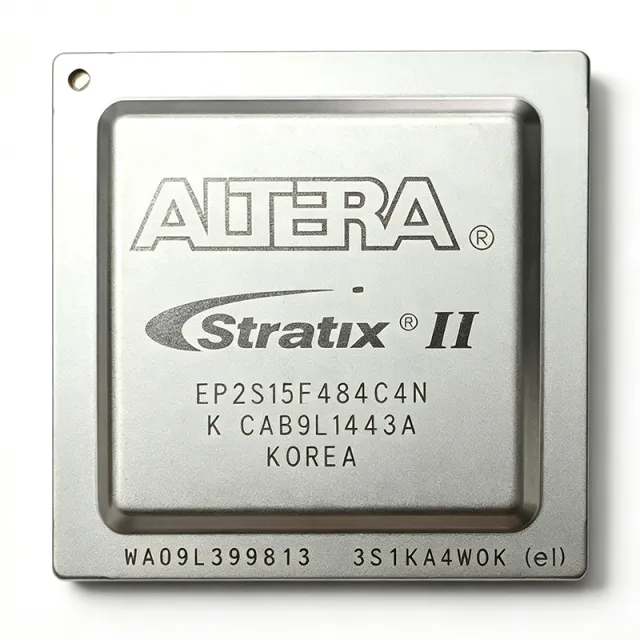
EP2S15F484C4 - Stratix II FPGA, 15.6K LEs, 484-FBGA | Intel
EP2S15F484C4 ⚠ Letzte Bestellmöglichkeit
Spezifikationsvergleich
| Parameter | EP2S15F484C4 | EP2S15F484I4N |
|---|---|---|
| Marke | Intel | Intel |
| Kategorie | FPGA & CPLD | FPGA & CPLD |
| Lebenszyklusstatus | Letzte Kaufgelegenheit | Obsolete |
| Lagerstatus | In Stock | In Stock |
| Stückpreis (USD) | $205,00 | $0,00 |
| Family | Stratix II | Stratix II |
| Logic Elements (LEs) | 15,600 | — |
| Adaptive Logic Modules (ALMs) / CLBs | 6,240 | — |
| Embedded Memory (Bits) | 419,328 | — |
| Maximum User I/O | 342 | — |
| DSP Blocks | Yes (integrated multiplier-accumulators) | — |
| Gehäuse | 484-FBGA (FBGA-484) | 484-BBGA |
| Package Dimensions | 23 mm x 23 mm | [DATA_NEEDED: package dimensions] |
| Ball Pitch | 1.0 mm | — |
| Process Technology | 90 nm CMOS | — |
| Core Performance | Up to 717 MHz | — |
| Speed Grade | C4 (-4, mid-tier) | — |
| Temperature Grade | Commercial (C): 0 C to +85 C junction | Industrial |
| Supply Voltage (Core) | [DATA_NEEDED: VCCINT nominal] | — |
| I/O Standards Supported | LVDS, LVTTL, LVCMOS, SSTL, HSTL | — |
| External Memory Interface | DDR, DDR2, QDR SRAM | — |
| Configuration Method | Serial/parallel, JTAG | — |
| RoHS-Status | Compliant (lead-free FBGA package) | [DATA_NEEDED: RoHS status] |
| Device Type | — | Field Programmable Gate Array (FPGA) |
| Logic Elements | — | 15,600 |
| Embedded Memory | — | 419,328 bits |
| User I/O Pins | — | 342 |
| Configurable Logic Blocks | — | 780 |
| Operating Voltage | — | 1.2 V |
| Terminal Count | — | 484 |
| Terminal Form | — | Ball |
| Package Shape | — | Square |
| Montageart | — | Surface Mount |
| REACH Status | — | [DATA_NEEDED: REACH status] |
| Maximale Taktfrequenz | — | [DATA_NEEDED: maximum clock frequency] |
| Betriebstemperaturbereich | — | [DATA_NEEDED: operating temperature range] |