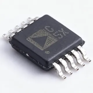
AD9804JST - 10-Bit 18 MSPS CCD Signal Processor | Analog Devices
Teilenummer: AD9804JST ✓ AktivAD9804JST Übersicht
An analog front-end, or AFE, is an integrated circuit positioned between an analog sensor and a digital processor. In a CCD imaging chain, the AFE extracts pixel information from the charge-transfer output, applies correlated double sampling to suppress noise and offset, adjusts signal amplitude through a variable-gain amplifier, and converts the conditioned waveform into digital data. The AD9804JST combines these stages into one low-power CMOS device.
The device provides 18 MSPS correlated-double-sampling operation, a 10-bit variable-gain amplifier covering 0 to 34 dB, low-noise clamp circuits, a preblanking function, and a 10-bit 18 MSPS ADC. Its three-wire serial interface programs VGA gain, allowing a camera system to adapt amplification while operating from the same single 3 V supply.
The AD9804 architecture is intended to reduce the external analog circuitry required around a CCD output. Correlated double sampling compares the CCD signal during reference and signal intervals, while the VGA restores small pixel amplitudes to a range suitable for digitization. The integrated ADC then produces 10-bit parallel digital data for capture by an image-processing or frame-grabber circuit.
Typical applications include consumer CCD cameras, surveillance cameras, industrial imaging equipment, document scanners, machine-vision cameras, and optical sensors that use interlaced or progressive-scan CCD arrays. Its integrated signal chain is particularly useful when designers need a compact camera front end without implementing separate sampling, gain, and conversion stages.
A critical design consideration is the timing relationship among CCD clocking, reset intervals, correlated-double-sampling timing, and ADC acquisition. The interface and control signals should be evaluated together with the camera sensor because improper timing can reduce image quality even when the electrical parameters are within limits. PCB placement should also keep the CCD signal path short and place bypassing capacitance close to the supply pins.
This page combines the device architecture, application guidance, package details, and practical design considerations with a clear explanation of drop-in alternatives. It is intended to help engineers evaluate whether the AD9804JST provides the required sampling rate, gain range, interface method, and package for a CCD imaging design before completing schematic and layout work.
Drop-in-Alternativen für AD9804JST – gleiches Gehäuse, Pin-kompatibel. Bauteile mit anderem Gehäuse, die eine PCB-Überarbeitung erfordern, sind ausgeschlossen.
AD9804AST
✅ Drop-In ⚠️ Spezifikationen ungeprüft📋 Referenzalternative (nicht im Katalog)
AD9804JST Grenzwerte & elektrische Eigenschaften
| Product Type | CCD analog front-end and signal processor |
| ADC Resolution | 10 bit |
| Abtastrate | 18 MSPS |
| CDS Processing Rate | 18 MSPS |
| Variable Gain Amplifier Range | 0 to 34 dB |
| Versorgungsspannung | 3 V |
| Supply Configuration | Single supply |
| Digital Interface | 3-wire serial interface |
| Signal Chain | Correlated double sampling, VGA, clamp, and ADC |
| Clamp Circuits | Low-noise clamp |
| Preblanking | Supported |
| Process Technology | CMOS |
| Gehäuse | 48-lead LQFP |
| Montageart | Surface mount |
| Sensor Compatibility | Interlaced and progressive-scan area CCD arrays |
AD9804JST 48-lead lqfp Pinbelegungsleitfaden
Pinbelegung für AD9804JST (48-lead lqfp-Gehäuse). Dieses analoge Bauteil verfügt über Eingangs-, Ausgangs- und Versorgungspins. Offset-Null-, Kompensations- und Enable-Pin-Konfigurationen entnehmen Sie dem Herstellerdatenblatt. Ideal für Signalaufbereitung und Verstärkerschaltungen.

Keine detaillierten Pinbelegungsdaten verfügbar für AD9804JST.
Siehe die Datenblatt für die vollständige Pin-Konfiguration.
Typische Anwendungen
AD9804JST ist geeignet für 6 Anwendungs: Consumer CCD Cameras, Surveillance Camera Front Ends, Industrial Machine Vision, Document Scanners, Optical Measurement Systems, Scientific and Laboratory Imaging.
Consumer CCD Cameras
The AD9804JST fits compact consumer CCD imaging chains that require pixel sampling, gain control, and digitization close to the sensor. Its integrated correlated-double-sampling path operates at 18 MSPS, while the 0 to 34 dB VGA compensates for scene-dependent signal amplitude. The 10-bit ADC then supplies digital pixel data to the camera processor. Because the device handles sampling, amplification, clamping, preblanking, and conversion in one 48-lead LQFP, it can reduce external analog components and shorten the sensitive CCD signal path. Designers should still validate CCD timing, gain programming, and power sequencing for the selected image sensor.
Empfohlen
Surveillance Camera Front Ends
The AD9804JST is suitable for surveillance camera electronics built around interlaced or progressive-scan area CCD arrays. Its 18 MSPS correlated double sampler and 10-bit conversion path support rapid pixel acquisition, while the programmable 0 to 34 dB VGA adapts to changes in scene illumination. The three-wire serial interface allows gain to be adjusted by the camera controller without adding a separate analog gain-control network. Its single 3 V operation simplifies the supply architecture in space-constrained camera housings. PCB implementation should minimize traces around CCD inputs and place bypass capacitors near the supply pins to reduce pickup and supply-noise effects.
Empfohlen
Industrial Machine Vision
The AD9804JST can support low-cost machine-vision systems that use area CCD sensors and require compact analog digitization. Its integrated CDS, VGA, clamp, preblanking, and 10-bit ADC functions replace several discrete signal-processing stages close to the sensor. The 18 MSPS processing rate supports fast pixel timing, and the 0 to 34 dB gain range helps maintain usable signal levels across changing lighting conditions. The three-wire interface allows the machine-vision controller to update VGA gain as part of an exposure-control routine. Confirm sensor timing compatibility, operating temperature, and digital data integration before using the part in a production machine-vision camera.
Empfohlen
Document Scanners
The AD9804JST is appropriate for CCD-based document scanners that need a consolidated sampling and conversion path. The correlated-double-sampling function operates at 18 MSPS and helps isolate the CCD pixel information from offset-related effects, while the integrated VGA offers 0 to 34 dB of programmable gain. A 10-bit ADC can feed a document image processor without requiring a separate high-speed converter in the immediate sensor path. The single 3 V supply and compact 48-lead LQFP package support board-space reduction. During development, coordinate scanner clock timing with the CDS and preblanking requirements, and verify the output encoding expected by the downstream image processor.
Empfohlen
Optical Measurement Systems
The AD9804JST can serve optical measurement systems built around compatible area CCD arrays where compact, low-power signal conditioning is valuable. Its 18 MSPS correlated-double-sampling stage, programmable 0 to 34 dB VGA, and 10-bit ADC create a unified path from CCD charge to digital samples. The three-wire interface permits system-level adjustment of gain without external potentiometers or a separate gain-control bus. Designers can use this flexibility to compensate for changes in illumination or optical alignment, although measurement accuracy still depends on sensor noise, clocking, and downstream calibration. Establish the analog grounding and impedance strategy before evaluating measurement uncertainty.
Empfohlen
Scientific and Laboratory Imaging
The AD9804JST is suitable for compact laboratory imaging systems that need a dedicated CCD sampling front end without the complexity of a large discrete analog chain. Its integrated 10-bit, 18 MSPS ADC, correlated double sampler, and 0 to 34 dB VGA shorten the path between the CCD and digital processing electronics. The programmable gain and three-wire control interface allow experimental configurations to be adjusted from the host processor. For scientific use, evaluate whether 10-bit resolution is adequate for the measurement range, and characterize sensor noise, offset, and linearity in the final mechanical and electrical assembly. Stable references and careful layout remain important for repeatable measurements.
Empfohlen
Zusammenfassung der empfohlenen Produkte
Technische Referenzdaten für AD9804JST – Vergleich, Designhinweise und Compliance-Informationen.
Auswahlhilfe
Vergleich mit Alternativen
| Parameter | Dieses Produkt | AD9804AST |
|---|---|---|
| Product Type | 10-bit CCD signal processor and analog front end | AD9804 CCD signal processor and analog front end |
| Brand | Analog Devices | Analog Devices |
| Package | 48-lead LQFP | 48-lead LQFP |
| ADC Resolution | 10 bit | 10 bit |
| Sampling Rate | 18 MSPS | 18 MSPS |
| Variable Gain Range | 0 to 34 dB | 0 to 34 dB |
| Supply Voltage | 3 V single supply | 3 V single supply |
| Control Interface | 3-wire serial interface | 3-wire serial interface |
Wichtigste Unterscheidungsmerkmale
- Complete CCD analog front end (vs. AD9804AST)
- Single 3 V integration (vs. AD9804AST)
- Programmable gain and preblanking (vs. AD9804AST)
Designhinweise
Keep the CCD signal path from the sensor to the AD9804JST as short and compact as practical. Place input decoupling and any return-path components according to the manufacturer application guidance rather than routing the analog signal through digital regions of the PCB. A continuous ground plane under the analog section can reduce loop area, but avoid high-current switching paths beneath CCD inputs.
Coordinate CDS, reset, and preblanking timing with the CCD sensor and image processor before finalizing the interface. The 18 MSPS sampling architecture is only useful when pixel intervals, reset windows, and gain updates are synchronized correctly. Treat the three-wire control lines as potentially active during sensitive sampling periods and route them away from the analog input where practical.
Use the 3 V supply rail specified for the device and place high-frequency bypass capacitance close to the supply and ground pins. Check power sequencing against downstream image processors, especially when the CCD output can be active before the ADC supply is valid. A quiet 3 V rail is especially valuable because the AD9804 combines low-level CCD sampling with gain and conversion stages on the same package.
Do not select the part only by its 18 MSPS conversion rate. The camera system must also satisfy the CCD output format, CDS timing, gain-control protocol, power requirements, and downstream digital interface. Review the manufacturer ordering guide and pin-description table to confirm the exact grade, exposed-lead configuration, and package details before releasing the PCB footprint.
Compliance-Informationen
The manufacturer product page and datasheet describe the AD9804 as a CMOS CCD signal processor. Specific RoHS, REACH, lead-free, halogen-free, and conflict-minerals declarations require confirmation from the current Analog Devices product documentation or declaration.