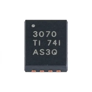
CD4050BF - 6-Channel CMOS Buffer, 3-18 V | Texas Instruments
Teilenummer: CD4050BF ✓ AktivCD4050BF Übersicht
A CMOS hex buffer is a digital logic device that receives six input signals and presents six buffered, non-inverting outputs. Buffers separate a source from its load, improve signal integrity, and can isolate logic levels when the input and output use different voltage references within the device operating range. In the CD4000 family hierarchy, the CD4050BF belongs to CMOS logic ICs and is commonly used as a line driver or logic-level converter.
The verified feature set includes six buffered channels, single-supply operation from 3 V to 18 V, non-inverting logic, and a military temperature range of -55 °C to 125 °C. Because it uses one supply voltage, the CD4050BF avoids the separate positive and negative reference rails historically associated with TTL-to-CMOS interface designs. This makes it useful where the source and destination circuits operate from the same supply but still benefit from output buffering.
The CD4050BF is based on the CD4050B family architecture and is intended for digital buffering rather than analog amplification. Its CMOS inputs provide high input impedance and minimize loading of the upstream device. Each output stage restores logic levels, helping maintain usable rise and fall times when driving additional CMOS inputs or cable capacitance.
Typical applications include industrial control and instrumentation, data acquisition, test equipment, legacy interface isolation, clock or signal distribution, and level translation within a 3 V to 18 V system. In instrumentation, the six channels can buffer sensor-conditioning outputs before they enter an ADC or counter. In control systems, the part can distribute buffered digital state signals among multiple receiver sections.
When designing around the CD4050BF, keep every connected signal within the specified input and output voltage limits, and do not exceed the 18 V maximum supply voltage. Decoupling close to the supply pins remains necessary for a CMOS device switching capacitive loads. Because the verified data does not provide a complete electrical characteristic table, propagation delay, output drive current, input leakage current, and logic-level thresholds should be confirmed in the manufacturer datasheet before release.
This page consolidates manufacturer and distributor references, validated CD4000-family equivalents, package-aware comparisons, and practical application guidance. It also identifies where the available sources do not publish a value, preventing unverified electrical specifications from being presented as guaranteed production data.
Drop-in-Alternativen für CD4050BF – gleiches Gehäuse, Pin-kompatibel. Bauteile mit anderem Gehäuse, die eine PCB-Überarbeitung erfordern, sind ausgeschlossen.
HEF4050BP
✅ Drop-In📋 Referenzalternative (nicht im Katalog)
HEF4050BT
✅ Drop-In📋 Referenzalternative (nicht im Katalog)
TC4050BP
✅ Drop-In📋 Referenzalternative (nicht im Katalog)
MC14050B
✅ Drop-In📋 Referenzalternative (nicht im Katalog)
HCF4050
✅ Drop-In📋 Referenzalternative (nicht im Katalog)
CD4050BF Grenzwerte & elektrische Eigenschaften
| Product Type | CMOS hex non-inverting buffer and logic-level converter |
| Number of Channels | 6 channels |
| Supply Voltage Range | 3 V to 18 V |
| Logic Type | Non-inverting |
| Betriebstemperaturbereich | -55 °C to 125 °C |
| Gehäuse | 16-pin CDIP (ceramic dual in-line) |
| Montageart | Through-hole |
| Technology | CMOS (CD4000 series) |
| Supply Configuration | Single supply |
| AEC-Q100 Qualification | Not applicable; this is a logic IC rather than an automotive-qualified device |
CD4050BF Pin-Konfiguration
| Pin 1 | 1A — Channel 1 non-inverting input |
| Pin 2 | 1Y — Channel 1 non-inverting output |
| Pin 3 | 2A — Channel 2 non-inverting input |
| Pin 4 | 2Y — Channel 2 non-inverting output |
| Pin 5 | 3A — Channel 3 non-inverting input |
| Pin 6 | 3Y — Channel 3 non-inverting output |
| Pin 7 | VSS — Ground supply |
| Pin 8 | 4A — Channel 4 non-inverting input |
| Pin 9 | 4Y — Channel 4 non-inverting output |
| Pin 10 | 5A — Channel 5 non-inverting input |
| Pin 11 | 5Y — Channel 5 non-inverting output |
| Pin 12 | 6A — Channel 6 non-inverting input |
| Pin 13 | 6Y — Channel 6 non-inverting output |
| Pin 14 | VDD — Positive supply |
| Pin 15 | NC — Not connected |
| Pin 16 | NC — Not connected |
Typische Anwendungen
CD4050BF ist geeignet für 6 Anwendungs: Industrial Control Signal Buffering, Data Acquisition Front-End, Legacy Logic-Level Translation, Test and Measurement Instrumentation, Clock and Digital Signal Distribution, Automotive and Aerospace Electronic Modules.
Industrial Control Signal Buffering
The CD4050BF suits industrial control boards where six digital control or status signals must reach multiple CMOS receiver sections without loading the source device. Its six non-inverting channels and 3 V to 18 V supply range allow operation across 5 V, 12 V, and 15 V control rails. Each buffer output isolates the originating logic gate from downstream wiring and input capacitance. The -55 °C to 125 °C specified range is appropriate for temperature-controlled industrial equipment, although propagation delay and output drive current must be checked in the TI datasheet. A short VDD-to-VSS bypass capacitor close to the package is recommended to limit supply transients when the outputs switch.
Empfohlen
Data Acquisition Front-End
The CD4050BF can isolate sensor, counter, or comparator outputs before they enter an ADC, microcontroller, or display driver. Six high-impedance CMOS inputs reduce loading on the source circuits, while the non-inverting outputs preserve the original logic polarity. Because the device operates from a single 3 V to 18 V supply, it fits systems where the sensor interface and acquisition logic share one rail. Its buffered outputs are preferable to directly connecting long PCB traces to multiple sensitive inputs. Engineers should confirm the input thresholds, output levels, and propagation delay at the actual VDD value because those parameters are not exposed in the verified search snippets.
Empfohlen
Legacy Logic-Level Translation
The CD4050BF is appropriate for single-supply logic-level conversion between CMOS domains that operate within its 3 V to 18 V range. The six buffered outputs can level-shift control or address signals while preventing the destination circuit from disturbing the source through back-feed or loading. The verified TI documentation identifies the CD4050B as a buffer and converter with single-supply operation. Since the available sources do not list the complete transfer curves or logic thresholds, each input-to-output voltage combination must be checked against the manufacturer electrical characteristics. Do not use the part for bipolar TTL levels without a suitable interface stage or level translation.
Empfohlen
Test and Measurement Instrumentation
The CD4050BF can buffer control and status lines in laboratory test equipment, programmable instruments, and automated test systems. Six channels allow one device to isolate several commands between a controller and analog or measurement subsystems. Its non-inverting behavior avoids changing the intended command polarity, while its 3 V to 18 V operating range supports legacy bench equipment operating from 5 V or 15 V supplies. The specified military temperature range also suits temperature-chamber and extended-temperature instrumentation. When driving long cables or connectorized inputs, verify output current and switching characteristics first, and provide local supply bypassing to preserve signal integrity at the measurement interface.
Empfohlen
Clock and Digital Signal Distribution
The CD4050BF can distribute one control signal to as many as six identical destinations, reducing fan-out loading on the original CMOS gate. Each non-inverting output provides a separate drive path, which is useful for clock-enable, handshake, latch, and counter-source signals distributed across a backplane or test fixture. The same part can distribute six separate one-bit signals because each channel is independent. Propagate the maximum expected frequency or edge rate and the receiver's input capacitance to determine whether the source must be divided or externally buffered. The published sources do not state propagation delay or transition time, so those values must come directly from the manufacturer datasheet.
Empfohlen
Automotive and Aerospace Electronic Modules
The CD4050BF's specified -55 °C to 125 °C operating range makes it relevant to industrial, aerospace, and legacy automotive electronic modules that require extended-temperature CMOS logic. Six channels can buffer inter-module control lines or interface signals in equipment operating from a single 3 V to 18 V supply. The ceramic CDIP package supports through-hole assembly and field replacement in legacy hardware. AEC-Q100 qualification is not established for the CD4050BF in the verified data, so automotive production use requires a separate qualification and traceability review. System engineers should also verify dielectric withstand, radiation requirements, temperature gradients, and output loading for their specific aerospace or automotive environment.
Empfohlen
Zusammenfassung der empfohlenen Produkte
Technische Referenzdaten für CD4050BF – Vergleich, Designhinweise und Compliance-Informationen.
Auswahlhilfe
Vergleich mit Alternativen
| Parameter | Dieses Produkt | HEF4050BP | HEF4050BT | TC4050BP | MC14050B | HCF4050 |
|---|---|---|---|---|---|---|
| Package | 16-CDIP | 16-CDIP | 16-CDIP | 16-CDIP | 16-CDIP | 16-CDIP |
| Brand | Texas Instruments | NXP Semiconductors | NXP Semiconductors | Microchip Technology | onsemi | STMicroelectronics |
| Channel Count | 6 channels | 6 channels | 6 channels | 6 channels | 6 channels | 6 channels |
| Logic Polarity | Non-inverting | Non-inverting | Non-inverting | Non-inverting | Non-inverting | Non-inverting |
Wichtigste Unterscheidungsmerkmale
- Original Texas Instruments CD4050B family sourcing with documented extended-temperature operation (vs. HEF4050BP)
- Six independent non-inverting buffered channels (vs. TC4050BP)
- Single-supply level conversion across a 3 V to 18 V operating range (vs. HCF4050)
Designhinweise
The verified operating range is 3 V to 18 V, so the VDD connection must never exceed 18 V. Place a high-frequency bypass capacitor close to VDD and connect it to the VSS reference with the shortest practical return path. The verified snippets do not include output current, quiescent current, or power dissipation, so calculate those values from the full manufacturer electrical characteristics before loading any output. Use local decoupling at the buffer rather than relying on supply wiring to isolate switching transients.
Treat all six CD4050BF inputs as high-impedance CMOS inputs and avoid excessive input capacitance or floating unused inputs. The six non-inverting outputs should drive CMOS receivers rather than bipolar TTL inputs, capacitive cables, LEDs, or relays without additional drive circuitry. Because propagation delay, transition time, and output drive current are not published in the verified snippets, check them in the manufacturer datasheet at the intended VDD and temperature before using the device for clock distribution or long interconnects.
Keep the VDD decoupling loop compact and separate the six output routes from sensitive analog inputs where possible. The CD4050BF is a digital buffer, not an analog amplifier, so unused channels should not be used for linear signal conditioning. The 16-CDIP through-hole package permits straightforward prototyping and socketed maintenance, but long socket or trace runs can increase susceptibility to noise. Keep signal wiring away from high-current switching nodes and verify ground continuity between the buffer and the receivers it serves.
Do not substitute a CD4049-family inverting part, and do not assume that identical CD4000-family logic functions guarantee identical thresholds, speed, drive strength, or temperature ratings. For each HEF4050, TC4050, MC14050, or HCF4050 alternative, verify the exact orderable suffix, package drawing, pinout, supply range, and electrical characteristics. Also note that the verified sources do not confirm RoHS, REACH, lead-free, or AEC-Q100 status for the CD4050BF.
Compliance-Informationen
The supplied verified snippets identify the TI CD4050B family, CD4000 CMOS technology, military temperature range, and packaging, but do not provide explicit RoHS, REACH, halogen-free, lead-free, or conflict-minerals declarations. These fields remain unknown rather than being inferred.