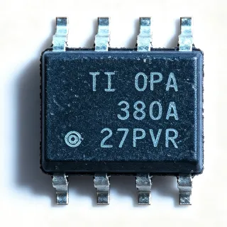
LM2904VQDRG4Q1 - 26V Dual Op Amp | Texas Instruments
Teilenummer: LM2904VQDRG4Q1 ✓ AktivLM2904VQDRG4Q1 Übersicht
An operational amplifier is an analog signal-conditioning IC that amplifies the voltage difference between its non-inverting and inverting inputs. The dual-amplifier configuration places two independent general-purpose amplifier channels in a common 8-pin SOIC package. Within the broader semiconductor hierarchy, this component is an operational amplifier, analog amplifier IC, and signal-conditioning IC commonly used to buffer sensors, amplify low-level signals, and support feedback-based circuit functions.
The principal characteristics include a 700 kHz gain-bandwidth product, 0.3 V/µs slew rate, maximum input offset voltage of 3 mV, and approximately 500 µA supply-current consumption per channel. These values make the LM2904VQDRG4Q1 appropriate for general-purpose analog signal paths where modest bandwidth, stable DC behavior, low quiescent current, and automotive qualification are more important than high-speed or precision performance.
Each channel contains an input stage, differential amplification function, and push-pull output stage designed for feedback operation. The 26 V total supply capability supports higher-voltage analog systems than common 5 V and 12 V precision amplifier families. Its 700 kHz gain-bandwidth product limits closed-loop bandwidth according to the selected noise gain, while the 0.3 V/µs slew rate limits large-signal transition speed. Applications must also observe the device's common-mode input, output swing, output-current, and stability limits from the manufacturer datasheet.
Typical uses include automotive sensor interfaces, low-frequency active filters, transducer signal conditioning, analog monitoring channels, and general-purpose buffering. The two channels can process related signals in one package, simplifying dual-channel analog front ends. In feedback networks, resistor ratios establish closed-loop gain, while output loading and source impedance determine practical bandwidth and stability performance.
A critical design consideration is power-supply bypassing. Place a suitable decoupling capacitor close to the supply pins and connect the ground return directly to the ground plane. Confirm input common-mode voltage, output swing, load current, and noise-gain stability against the datasheet limits before using the amplifier with large capacitive loads or high source impedances.
This product page combines the exact automotive ordering information, package and electrical characteristics, qualified drop-in alternatives, and practical design guidance into one engineering reference. It is intended to accelerate component selection, PCB footprint confirmation, and analog-circuit qualification for automotive and industrial designs.
Drop-in-Alternativen für LM2904VQDRG4Q1 – gleiches Gehäuse, Pin-kompatibel. Bauteile mit anderem Gehäuse, die eine PCB-Überarbeitung erfordern, sind ausgeschlossen.
Varianten dieser Serie
Modelle derselben Serie, die drop-in-kompatibel sind mit LM2904VQDRG4Q1 (gleiche Bauform und Footprint) – abweichend in Package, Automotive Qualification, Gain-Bandwidth Product, Input Offset Voltage, Slew Rate.
LM2904QDRQ1
✅ Drop-In ⚠️ Spezifikationen ungeprüft✓ Auf Lager
$0.22 / Stück
Datenblatt ansehen →LM2904BDR
✅ Drop-In ⚠️ Spezifikationen ungeprüft📋 Referenzalternative (nicht im Katalog)
LM2904BADR
✅ Drop-In ⚠️ Spezifikationen ungeprüft📋 Referenzalternative (nicht im Katalog)
LM2904BVQDRG4Q1
✅ Drop-In ⚠️ Spezifikationen ungeprüft📋 Referenzalternative (nicht im Katalog)
LM2904BAVQDRG4Q1
✅ Drop-In ⚠️ Spezifikationen ungeprüft📋 Referenzalternative (nicht im Katalog)
LM2904VQDRG4Q1 Grenzwerte & elektrische Eigenschaften
| Amplifier Type | General-purpose operational amplifier |
| Number of Circuits | 2 circuits |
| Versorgungsspannung | 26 V maximum |
| Gain-Bandwidth Product | 700 kHz |
| Slew Rate | 0.3 V/µs |
| Input Offset Voltage | 3 mV maximum |
| Supply Current per Channel | 500 µA typical |
| Betriebstemperaturbereich | -40°C to 125°C |
| Automotive Qualification | AEC-Q100 qualified |
| Gehäuse | 8-SOIC (D) |
| Anzahl der Pins | 8 pins |
| Montageart | Surface mount |
| Packaging | Tape and reel |
| Product Type | Dual operational amplifier |
| Low-Supply-Current Drain | Independent of supply voltage |
LM2904VQDRG4Q1 8-soic (d) Pinbelegungsleitfaden
Pinbelegung für LM2904VQDRG4Q1 (8-soic (d)-Gehäuse). Dieses analoge Bauteil verfügt über Eingangs-, Ausgangs- und Versorgungspins. Offset-Null-, Kompensations- und Enable-Pin-Konfigurationen entnehmen Sie dem Herstellerdatenblatt. Ideal für Signalaufbereitung und Verstärkerschaltungen.

Keine detaillierten Pinbelegungsdaten verfügbar für LM2904VQDRG4Q1.
Siehe die Datenblatt für die vollständige Pin-Konfiguration.
Typische Anwendungen
LM2904VQDRG4Q1 ist geeignet für 6 Anwendungs: Automotive Sensor Signal Conditioning, Dual-Channel Buffering, Active Filter and Audio Interface, Industrial Transducer Interface, Power Supply Feedback and Monitoring, Portable and Battery-Powered Analog Module.
Automotive Sensor Signal Conditioning
The LM2904VQDRG4Q1 is suitable for amplifying weak sensor signals in automotive electronic control modules because its two channels, 700 kHz gain-bandwidth product, and AEC-Q100 qualification align with general-purpose analog front-end requirements. A typical circuit uses one channel for amplification and the other for buffering or active filtering. The 3 mV maximum input offset and 0.3 V/µs slew rate provide useful limits for designing closed-loop gain stages. Confirm common-mode input range and output swing against the manufacturer datasheet, especially when the sensor operates near a supply rail. Place the device away from high-current switching paths and use short, guarded signal traces to reduce automotive EMI coupling.
Empfohlen
Dual-Channel Buffering
The dual-channel architecture of the LM2904VQDRG4Q1 allows two independent buffers to be placed in one 8-SOIC package, reducing board area in monitoring and control systems. Its 700 kHz gain-bandwidth product is suitable for low-to-moderate bandwidth signals, while approximately 500 µA of supply-current consumption per channel supports power-conscious designs. Configure each channel as a voltage follower when isolation between a source and the next circuit stage is required. Keep source impedances low enough to avoid amplifier-induced errors, and verify that the load current and capacitive loading remain within the manufacturer limits. The -40°C to 125°C rating makes the part suitable for industrial environments as well as qualified automotive designs.
Empfohlen
Active Filter and Audio Interface
The LM2904VQDRG4Q1 can implement first-order active filters, gain stages, and low-frequency audio interface functions when the system does not require rail-to-rail inputs or high slew performance. Its 700 kHz gain-bandwidth product allows useful closed-loop bandwidth in low-gain configurations, while the 0.3 V/µs slew rate helps define large-signal behavior. Two channels can form a cascaded filter or provide independent signal paths. Select resistor values so the operating frequency remains well below amplifier bandwidth, and assess phase margin for the actual noise gain. For longer boards or systems near motors and switching regulators, compare the LM2904BA family, which adds integrated EMI/RF filtering, before finalizing the analog front end.
Empfohlen
Industrial Transducer Interface
The LM2904VQDRG4Q1 is appropriate for general-purpose industrial transducer interfaces that require two low-frequency amplification channels in a compact SOIC package. The 26 V supply rating permits operation from higher-voltage analog rails, and the -40°C to 125°C temperature range covers extended industrial environments. A practical implementation may amplify a bridge or resistive sensor on one channel and provide an active filter or reference buffer on the other. The 3 mV maximum offset voltage is an important error budget component when the sensor signal is small. Confirm the common-mode input range, output swing, input bias current, and noise behavior against the manufacturer datasheet, then isolate high-impedance sensor nodes from noisy power and switching traces.
Empfohlen
Power Supply Feedback and Monitoring
The LM2904VQDRG4Q1 can support low-frequency power-supply monitoring, error amplification, or feedback assistance in systems using a 26 V-class analog rail. Its two channels permit a comparison amplifier and an output-buffer stage to share one package. The 700 kHz gain-bandwidth product is appropriate for slow supervisory loops rather than high-frequency compensation, and the 0.3 V/µs slew rate limits how quickly the output can follow large corrections. Account for input offset voltage, common-mode limits, and output saturation when defining fault thresholds. Decouple the supply pins locally, connect the ground reference directly to the power ground plane, and test the complete loop for stability under load transients before using the amplifier in a control path.
Empfohlen
Portable and Battery-Powered Analog Module
Approximately 500 µA of supply-current consumption per channel makes the LM2904VQDRG4Q1 relevant to battery-powered instrumentation where each amplifier channel must operate from a shared 8-SOIC package. The dual configuration can reduce component count in sensor interfaces, threshold detectors, and low-frequency filter stages. Its low supply-current drain is described as independent of supply voltage, although total system consumption still includes input bias current and load effects. Use a stable low-noise supply and place local bypass capacitance close to the device. Avoid designs requiring rail-to-rail input or output operation unless the specific input and output ranges are verified. The -40°C to 125°C rating also permits use in temperature-varying industrial or automotive modules.
Empfohlen
Zusammenfassung der empfohlenen Produkte
Technische Referenzdaten für LM2904VQDRG4Q1 – Vergleich, Designhinweise und Compliance-Informationen.
Auswahlhilfe
Vergleich mit Alternativen
| Parameter | Dieses Produkt | LM2904QDR | LM2904BDR | LM2904BADR | LM2904BVQDRG4Q1 | LM2904BAVQDRG4Q1 |
|---|---|---|---|---|---|---|
| Brand | Texas Instruments | Texas Instruments | Texas Instruments | Texas Instruments | Texas Instruments | Texas Instruments |
| Package | 8-SOIC (D) | 8-SOIC (D) | 8-SOIC (D) | 8-SOIC (D) | 8-SOIC (D) | 8-SOIC (D) |
| Number of Circuits | 2 circuits | 2 circuits | 2 circuits | 2 circuits | 2 circuits | 2 circuits |
| Supply Voltage | 26 V | 26 V | 36 V | 36 V | 36 V | 36 V |
| Gain-Bandwidth Product | 700 kHz | 700 kHz | 1.2 MHz | 1.2 MHz | 1.2 MHz | 1.2 MHz |
| Supply Current per Channel | 500 µA typical | 500 µA typical | 300 µA typical | 300 µA typical | 300 µA typical | 300 µA typical |
| Integrated EMI/RF Filtering | No | No | No | Yes | No | Yes |
Wichtigste Unterscheidungsmerkmale
- Original-family performance with automotive qualification (vs. LM2904BDR)
- Lower quiescent current than the B family (vs. LM2904BVQDRG4Q1)
- No integrated EMI/RF input filter (vs. LM2904BAVQDRG4Q1)
Designhinweise
Place the supply bypass capacitor immediately between the 8-SOIC supply and ground pins, with a short return path to the ground plane. The 26 V supply rating does not permit unlimited rail tolerance; validate transients and automotive load-dump requirements against the manufacturer limits before energizing the circuit. Avoid adding large supply capacitors without checking whether their effective series inductance can produce oscillation with the amplifier’s output capability.
Keep non-inverting input routes short and away from the output node to prevent parasitic feedback. For high-impedance sensors, minimize leakage paths and guard the input node where appropriate. A solid ground plane beneath the device provides a low-impedance return, while keeping power-supply routing and switching-node copper separated from the analog input path reduces coupling into the 3 mV input-offset budget.
Do not assume rail-to-rail input or output behavior. Verify the common-mode input range, output swing, output-current capability, and stability behavior from the manufacturer datasheet for the selected configuration. The 700 kHz gain-bandwidth product and 0.3 V/µs slew rate are suitable for low-frequency general-purpose operation but may be insufficient for demanding precision, high-speed, or capacitive-load applications.
Assess each closed-loop configuration using the actual noise gain rather than the signal gain alone. Large feedback resistors increase Johnson noise and can interact with input capacitance to shift poles or reduce phase margin. Add a practical feedback resistor near the amplifier when bias-current compensation is needed, and use small capacitors or additional stages only after checking their effect on stability and offset.
Compliance-Informationen
Texas Instruments states that the LM2904-Q1 family is qualified for automotive use in accordance with AEC-Q100 specifications. Other environmental and material-compliance statuses are not established by the cited product-page excerpts.