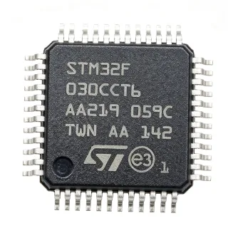
PIC24F08KM202-I/ML - 32MHz Low-Power MCU | Microchip
Teilenummer: PIC24F08KM202-I/ML ✓ AktivPIC24F08KM202-I/ML Übersicht
A PIC24F microcontroller is a compact embedded-processing platform that combines a CPU core, nonvolatile program memory, volatile data memory, and programmable peripherals in one package. Within the broader semiconductor hierarchy, it belongs to the MCU and embedded-controller family rather than a general-purpose microprocessor. The PIC24F KM series is specifically positioned for low-power applications requiring analog conversion, signal conditioning, and digital control in small pin-count packages.
Key features include 8 KB of Flash memory organized as 2.75K x 24 words, 2 KB of RAM, and 512 bytes of EEPROM. The device combines a 12-bit ADC with a DAC, operational amplifiers, comparators, and CLC peripherals, reducing the need for external analog components in measurement and control systems. Its 1.8 V to 5.5 V operating range supports low-voltage industrial, consumer, and embedded applications.
The 28-QFN package provides a compact 6 x 6 mm footprint with an exposed pad for board-level thermal management. The PIC24 architecture supports a 32 MHz clock while retaining the feature set expected from an XLP-oriented low-power design. This combination makes the MCU suitable for local sensing, control-loop execution, signal conversion, and communications-oriented embedded nodes where component count and board area are important.
Typical applications include industrial sensor nodes, compact control panels, portable instrumentation, battery-powered monitoring systems, consumer controls, and embedded motor or actuator controllers. The integrated ADC and analog peripherals support direct measurement of analog inputs, while the DAC, comparators, operational amplifiers, and CLC can assist with signal generation, threshold detection, conditioning, and programmable logic functions.
Designers should account for the exposed-pad thermal path when assigning the package on the PCB and should follow the manufacturer’s land-pattern and decoupling guidance. The 1.8 V to 5.5 V operating range requires careful selection of external component ratings, programming-tool compatibility, and logic levels. Confirm the device’s complete pin assignment and peripheral multiplexing in the Microchip product documentation before finalizing a new layout.
This page organizes the key electrical, memory, analog, package, and sourcing information for the PIC24F08KM202-I/ML while providing practical application guidance, drop-in alternatives, comparison parameters, and design notes. It supports faster engineering evaluation without replacing the complete manufacturer datasheet, reference manual, or device programming documentation.
Drop-in-Alternativen für PIC24F08KM202-I/ML – gleiches Gehäuse, Pin-kompatibel. Bauteile mit anderem Gehäuse, die eine PCB-Überarbeitung erfordern, sind ausgeschlossen.
Varianten dieser Serie
Modelle derselben Serie, die drop-in-kompatibel sind mit PIC24F08KM202-I/ML (gleiche Bauform und Footprint) – abweichend in Package, Program Memory (Flash), ADC, Core Architecture, DAC.
PIC24F08KM202-E/ML
✅ Drop-InPreis auf Anfrage
Datenblatt ansehen →PIC24F08KM202T-I/ML
✅ Drop-InPreis auf Anfrage
Datenblatt ansehen →PIC24F08KM202-I/ML Grenzwerte & elektrische Eigenschaften
| Product Type | 16-bit low-power microcontroller (MCU) |
| Maximum CPU Frequency | 32 MHz |
| Flash Program Memory | 8 KB (2.75K x 24 words) |
| RAM | 2 KB |
| EEPROM | 512 bytes |
| Operating Voltage Range | 1.8 V to 5.5 V |
| ADC Resolution | 12 bits |
| Integrated DAC | Yes |
| Integrated Operational Amplifiers | Yes |
| Integrated Comparators | Yes |
| Configurable Logic Cell | Yes |
| Architecture | PIC24F 16-bit RISC |
| Gehäuse | 28-QFN, 6 x 6 mm |
| Montageart | Surface mount |
| Temperature Grade | Industrial grade |
| Exposed Pad | Present |
PIC24F08KM202-I/ML 28-qfn, 6 x 6 mm Pinbelegungsleitfaden
Pinbelegung für PIC24F08KM202-I/ML (28-qfn, 6 x 6 mm-Gehäuse). Dieser digitale IC umfasst GPIO, Kommunikationsschnittstellen (UART, SPI, I2C) und Versorgungspins. Alternative Pin-Funktionen und Konfigurationsoptionen entnehmen Sie dem Herstellerdatenblatt. Unverzichtbar für Embedded-System-Design und PCB-Layout.

Keine detaillierten Pinbelegungsdaten verfügbar für PIC24F08KM202-I/ML.
Siehe die Datenblatt für die vollständige Pin-Konfiguration.
Typische Anwendungen
PIC24F08KM202-I/ML ist geeignet für 6 Anwendungs: Low-Voltage Industrial Sensor Node, Portable Battery-Powered Instrumentation, Compact Control Panel, Programmable Threshold Detection, Consumer Control and Interface Module, Compact Data-Acquisition Module.
Low-Voltage Industrial Sensor Node
The PIC24F08KM202-I/ML fits compact sensor nodes that must acquire analog measurements while retaining low-power operation across a 1.8 V to 5.5 V range. Its 12-bit ADC supports direct conversion of temperature, pressure, or level signals, while the 32 MHz PIC24F core provides enough execution speed for filtering, calibration, and local control. The 8 KB Flash and 2 KB RAM are suitable for focused firmware rather than resource-heavy applications. Integration of comparators, op amps, and CLC logic can reduce external conditioning components. Place the MCU near the sensor interface, follow the manufacturer’s exposed-pad land pattern, and reserve stable decoupling for the analog and digital supplies.
Empfohlen
Portable Battery-Powered Instrumentation
The PIC24F08KM202-I/ML is appropriate for portable instrumentation because the PIC24F KM family supports operation from 1.8 V to 5.5 V and combines control and analog functions in one compact device. The 12-bit ADC can acquire sensor data, the DAC can generate an analog reference or test stimulus, and the operational amplifiers can assist with conditioning. With 8 KB Flash, 2 KB RAM, and 512 bytes of EEPROM, the device targets focused instruments rather than large data-logging systems. Low-power design should include sleep-mode firmware, peripheral shutdown, and careful control of analog bias currents to extend battery life.
Empfohlen
Compact Control Panel
A PIC24F08KM202-I/ML-based control panel can combine button or encoder input, analog setpoint measurement, status indication, and actuator control in a small board. The 32 MHz processor supports responsive state-machine control, while the 12-bit ADC handles analog controls and sensor inputs. Integrated comparators can perform fast threshold detection, and the CLC can combine programmable logic functions without consuming a separate logic device. The 28-QFN 6 x 6 mm package saves board area but requires careful escape routing and exposed-pad thermal management. Firmware should account for debounce timing, input protection, and output update latency.
Empfohlen
Programmable Threshold Detection
The PIC24F08KM202-I/ML is suitable for programmable threshold and window-detection systems because it combines a 12-bit ADC, comparators, operational amplifiers, and a Configurable Logic Cell. The ADC can monitor a slowly varying sensor signal, while comparator inputs can react to faster edges. The CLC can implement programmable Boolean relationships, reducing the need for external logic in alarm, protection, or event-detection products. The 1.8 V minimum operating voltage supports low-energy systems, although analog input, output, and supply voltages must remain within the device’s specified limits. Validate threshold accuracy and noise behavior across temperature before using a comparator for safety-critical decisions.
Empfohlen
Consumer Control and Interface Module
The PIC24F08KM202-I/ML can support compact consumer-control modules that combine local input handling, analog sensing, and low-speed peripheral control. Its 2 KB RAM and 8 KB Flash are appropriate for focused tasks such as configuring a display, reading controls, updating indicators, and managing a simple actuator. Integrated DAC and op-amp resources can generate test signals or support limited audio and analog functions, while the 32 MHz core allows time-sensitive control routines. The wide 1.8 V to 5.5 V operating range supports multiple system rails, but peripheral interfaces and external logic levels must be checked against the selected operating voltage.
Empfohlen
Compact Data-Acquisition Module
The PIC24F08KM202-I/ML can serve as the controller for a compact data-acquisition module built around a small number of analog channels. The integrated 12-bit ADC handles sampled inputs, while the DAC provides a low-resolution excitation or calibration output. Its 32 MHz maximum frequency supports timing and control tasks, and 512 bytes of EEPROM can retain configuration values. The 2 KB RAM limit makes streaming large sample buffers impractical, so designs should batch measurements or use an external storage interface if required. Keep analog routing short, maintain defined grounding between analog and digital sections, and follow the manufacturer’s grounding and decoupling layout practices.
Empfohlen
Zusammenfassung der empfohlenen Produkte
Technische Referenzdaten für PIC24F08KM202-I/ML – Vergleich, Designhinweise und Compliance-Informationen.
Auswahlhilfe
Vergleich mit Alternativen
| Parameter | Dieses Produkt | PIC24F08KM202-E/ML | PIC24F08KM202T-I/ML |
|---|---|---|---|
| Brand | Microchip Technology | Microchip Technology | Microchip Technology |
| Package | 28-QFN (6x6) | 28-QFN (6x6) | 28-QFN (6x6) |
| Maximum CPU Frequency | 32 MHz | 32 MHz | 32 MHz |
| Flash Program Memory | 8 KB (2.75K x 24 words) | 8 KB | 8 KB |
Wichtigste Unterscheidungsmerkmale
- Retains identical core frequency and program-memory capacity versus the E-grade candidate (vs. PIC24F08KM202-E/ML)
- Retains identical core frequency and program-memory capacity versus the T-I candidate (vs. PIC24F08KM202T-I/ML)
- Combines control and analog resources in a compact package (vs. PIC24F08KM202-E/ML)
Designhinweise
The 28-QFN package includes an exposed pad that must be connected according to the manufacturer’s package drawing. Provide a continuous thermal copper path to the board ground plane with minimal thermal breaks, and keep high-current or temperature-sensitive analog routing away from the pad region. Because the exact package thermal resistance is not stated, thermal qualification should use measured board performance or manufacturer-provided guidance rather than an assumed junction-temperature margin.
Follow the official 28-QFN land pattern and pin table when assigning traces and vias. Place input and output decoupling capacitors close to their designated supply pins, with the shortest practical return path to the associated ground reference. The exposed pad should not be treated as an arbitrary mechanical ground connection; use the manufacturer’s pin designation and layout instructions to determine its electrical treatment.
Separate sensitive analog inputs from fast digital clocks and switching nodes, particularly when the 12-bit ADC is used near the device’s maximum operating frequency. Route analog signals over a continuous ground reference, keep the analog and digital return currents controlled, and avoid sharing narrow necks between analog and digital paths. Validate gain, offset, and noise performance on the final PCB because pad and via parasitics can affect measurements even when the MCU configuration is unchanged.
Do not treat the -I/ML, -E/ML, and -T-I/ML suffixes as interchangeable without checking the required temperature and qualification limits. Although all identified candidates use the 28-QFN footprint and retain the 32 MHz, 8 KB-Flash basis, ordering-grade differences can affect deployment conditions. Also verify the programming interface, peripheral multiplexing, and exposed-pad connection in the manufacturer documentation before releasing a production PCB.
Compliance-Informationen
Compliance statements were not established for this ordering suffix. Confirm RoHS, REACH, lead-free, halogen-free, and conflict-mineral status with Microchip for the exact part number and current material declaration.