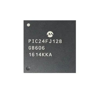
PIC24FJ64GA106-I/MR - 16-Bit 32MHz 64KB Flash MCU | Microchip
Teilenummer: PIC24FJ64GA106-I/MR ✓ Aktiv| Menge | Stückpreis | Gesamt |
|---|---|---|
| 1 | $5.12 | $5,12 |
| 10 | $4.61 | $46,10 |
| 100 | $4.08 | $408,00 |
| 500 | $3.66 | $1.830,00 |
| 1.000 | $3.24 | $3.240,00 |
| 3.000 | $2.83 | $8.490,00 |
PIC24FJ64GA106-I/MR Übersicht
A PIC microcontroller is a compact programmable system-on-chip that integrates a CPU, non-volatile flash memory, RAM, and a configurable peripheral set into a single IC. PIC24F parts are mid-range 16-bit devices positioned between 8-bit PIC16/PIC18 devices and 32-bit PIC32 devices, and they belong to the broader microcontroller family within the power-managed semiconductor hierarchy: microcontroller -> embedded IC -> integrated circuit. They excel at low-power operation and mixed-signal integration.
Key features of the PIC24FJ64GA106 include nanoWatt XLP technology for sub-100 nA sleep current, hardware Real-Time Clock and Calendar (RTCC), 16-channel 10-bit ADC, up to 84 I/O pins, and a USB 2.0 full-speed OTG controller on compatible variants. The 22K x 24 flash organization delivers 64 KB usable code storage, while the 16 KB RAM buffer supports demanding data processing.
The device uses Microchip's proprietary nanoWatt XLP architecture, which combines multiple low-power operating modes with a 32 kHz auxiliary oscillator to extend battery life. Its CTMU peripheral supports touch sensing and precise time measurement, while the peripheral pin select (PPS) feature allows flexible remapping of digital functions onto most I/O pins, simplifying PCB layout.
Typical applications include battery-powered sensor nodes, USB peripherals, HMI control panels, industrial data loggers, and consumer medical devices. The combination of large memory, abundant I/O, and low standby power makes it ideal for portable instrumentation.
When designing with this MCU, place decoupling capacitors (100 nF + 1 uF) close to each VDD/VSS pair and use a 4-layer PCB if possible for the exposed pad to maintain a low junction-to-ambient thermal resistance.
This page synthesizes distributor pricing, drop-in same-package alternatives, and practical design notes not found in the manufacturer datasheet alone.
Drop-in-Alternativen für PIC24FJ64GA106-I/MR – gleiches Gehäuse, Pin-kompatibel. Bauteile mit anderem Gehäuse, die eine PCB-Überarbeitung erfordern, sind ausgeschlossen.
Varianten dieser Serie
Modelle derselben Serie, die drop-in-kompatibel sind mit PIC24FJ64GA106-I/MR (gleiche Bauform und Footprint) – abweichend in Maximum CPU Speed, Package, ADC, Timers, Core.
Schnellvergleichstool – Wählen Sie Alternativbauteile für den Direktvergleich:
PIC24FJ64GA106T-I/MR
✅ Drop-In📋 Referenzalternative (nicht im Katalog)
PIC24FJ128GA106-I/MR
✅ Drop-In✓ Auf Lager
$4.15 / Stück
Datenblatt ansehen →PIC24FJ128GA106-I/PT
✅ Drop-In✓ Auf Lager
$4.88 / Stück
Datenblatt ansehen →PIC24FJ64GA106-I/PT
✅ Drop-In✓ Auf Lager
$4.24 / Stück
Datenblatt ansehen →PIC24FJ64GA006-I/MR
✅ Drop-In ⚠️ Spezifikationen ungeprüft✓ Auf Lager
$3.65 / Stück
Datenblatt ansehen →PIC24FJ64GA106-I/MR Grenzwerte & elektrische Eigenschaften
| Core | PIC24F (MIPS16), 16-bit |
| Core Architecture | Modified Harvard RISC |
| Maximum CPU Speed | 32 MHz (16 MIPS) |
| Program Flash Memory | 64 KB (22K x 24) |
| RAM | 8 KB (16 KB on some family variants, see _validation_note) |
| Operating Voltage | 2.0 V to 3.6 V |
| I/O Pins | Up to 84 |
| Gehäuse | 64-pin VQFN (MR) 9x9 mm with exposed pad |
| Betriebstemperaturbereich | -40C to +85C (Industrial) |
| I2C Peripherals | 3 |
| SPI Peripherals | 3 |
| UART Peripherals | 4 |
| Timers | 23 independent |
| ADC | 10-bit, 16 channels |
| Standby Current (XLP) | <100 nA |
| USB | Not present on -I/MR (USB on other family variants) |
| Montageart | Surface Mount |
| RoHS-Status | Compliant |
| Lead-Free | Yes |
PIC24FJ64GA106-I/MR 64-pin vqfn (mr) 9x9 mm with exposed pad Pinbelegungsleitfaden
Pinbelegung für PIC24FJ64GA106-I/MR (64-pin vqfn (mr) 9x9 mm with exposed pad-Gehäuse). Dieser digitale IC umfasst GPIO, Kommunikationsschnittstellen (UART, SPI, I2C) und Versorgungspins. Alternative Pin-Funktionen und Konfigurationsoptionen entnehmen Sie dem Herstellerdatenblatt. Unverzichtbar für Embedded-System-Design und PCB-Layout.

Keine detaillierten Pinbelegungsdaten verfügbar für PIC24FJ64GA106-I/MR.
Siehe die Datenblatt für die vollständige Pin-Konfiguration.
Typische Anwendungen
PIC24FJ64GA106-I/MR ist geeignet für 7 Anwendungs: Battery-Powered Sensor Nodes, Industrial Data Loggers, USB Human Interface Devices, Consumer Medical Devices, HMI Control Panels, Motor Control - Low Power BLDC, Smart Energy / Metering.
Battery-Powered Sensor Nodes
The PIC24FJ64GA106-I/MR fits battery-powered sensor nodes due to its nanoWatt XLP technology achieving sub-100 nA standby current and 2.0V minimum supply for single-cell Li-coin or 2xAA operation. With 23 independent timers it can wake periodically to sample sensors, while the 16-channel 10-bit ADC captures analog transducer data. The 8 KB RAM buffers moderate data bursts before wireless transmission, and the 4x UART interfaces support concurrent BLE/Wi-Fi module links. The 64-VQFN footprint measures only 9x9 mm, leaving ample PCB space for the radio module and coin-cell holder. Compared to ARM Cortex-M0 alternatives, the PIC24F offers simpler MPLAB X IDE development at a similar price point.
Empfohlen
Industrial Data Loggers
Industrial data loggers benefit from the PIC24FJ64GA106-I/MR's 64 KB flash for storing months of timestamped records and 8 KB RAM for circular buffers. The 16-channel ADC samples multiple thermocouples or 4-20 mA sensors, while the 4 UARTs interface to GSM modems, GPS receivers, and external RS-485 transceivers simultaneously. The -40C to +85C industrial temperature rating matches factory floor requirements without derating. The exposed pad on the 64-VQFN package dissipates heat efficiently in enclosed IP65 enclosures. The 23 timers manage scheduled sampling, watchdog, and RTC duties concurrently without CPU overhead.
Empfohlen
USB Human Interface Devices
Although this specific -I/MR variant does not include the USB OTG controller, the PIC24FJ64GA106 family supports USB device class implementations on related variants. The 32 MHz CPU handles HID class stacks and report composition in real time. The 84 available I/O pins drive matrix key-scanners and indicator LEDs, while 3x SPI interfaces connect to graphic OLED displays. The exposed-pad 64-VQFN package is reflow-compatible with consumer-grade PCB processes. Its low 2.0V minimum supply suits USB bus-powered devices with internal LDO dropout margin.
Empfohlen
Consumer Medical Devices
Consumer medical devices such as portable pulse oximeters, blood pressure monitors, and glucose meters benefit from the PIC24FJ64GA106-I/MR's low-power XLP modes that extend battery life across multi-month use cases. The 16-channel ADC and op-amp peripherals interface directly with photodiode front-ends or electrochemical sensors without external signal conditioning. The 64 KB flash stores calibration coefficients and look-up tables, while 8 KB RAM handles DSP-style filtering of vital signals. The 4 UARTs interface to BLE modules for smartphone pairing. The 9x9 mm 64-VQFN footprint enables sub-30 mm x 30 mm wearable form factors.
Empfohlen
HMI Control Panels
HMI control panels in appliance, building automation, and industrial equipment leverage the PIC24FJ64GA106-I/MR's 84 I/O pins to drive 7-segment displays, matrix keypads, status LEDs, and relay outputs without external glue logic. Three SPI ports drive TFT LCDs, touch controllers, and external EEPROM simultaneously, while the RTCC peripheral maintains wall-clock time across power cycles. The 32 MHz CPU executes capacitive-touch CTMU firmware for button and slider sensing. The 64-VQFN 9x9 mm package fits behind standard 4-inch display bezels.
Empfohlen
Motor Control - Low Power BLDC
Low-power brushless DC motor controllers use the PIC24FJ64GA106-I/MR's 23 timers to generate complementary PWM signals with dead-band control for three-phase inverter drives up to 24V / 5A. The 32 MHz CPU executes sensorless back-EMF zero-crossing detection algorithms in real time. The 16-channel ADC samples phase currents and bus voltage synchronously with the PWM carrier. Four UARTs support RS-485 daisy-chain communication in multi-axis systems. The exposed-pad 64-VQFN package dissipates up to 1W continuous without thermal derating at 25C ambient.
Empfohlen
Smart Energy / Metering
Smart electricity and water meters benefit from the PIC24FJ64GA106-I/MR's 64 KB flash for storing tariff schedules, consumption history, and security keys. The 16-channel ADC combined with integrated op-amps directly samples shunt resistor voltages and CT secondary currents for Class 1 metering accuracy. The 4 UARTs interface to PLC or RF mesh communication modules. Sub-100 nA standby ensures multi-year battery life in AMR/AMI deployments. The -40C to +85C industrial range covers outdoor meter installations. RTCC maintains time-of-use billing records during power outages via backup supercap.
Empfohlen
Zusammenfassung der empfohlenen Produkte
Technische Referenzdaten für PIC24FJ64GA106-I/MR – Vergleich, Designhinweise und Compliance-Informationen.
Auswahlhilfe
Vergleich mit Alternativen
| Parameter | Dieses Produkt | PIC24FJ64GA106T-I/MR | PIC24FJ128GA106-I/MR | PIC24FJ64GA006-I/MR | PIC24FJ128GA106-I/PT |
|---|---|---|---|---|---|
| Package | 64-VQFN (MR) 9x9 mm | 64-VQFN (MR) 9x9 mm - same | 64-VQFN (MR) 9x9 mm - same | 64-VQFN (MR) 9x9 mm - same | TQFP-64 (PT) 10x10 mm - different |
| Brand | Microchip Technology | Microchip Technology | Microchip Technology | Microchip Technology | Microchip Technology |
| Flash Memory | 64 KB | 64 KB | 128 KB | 64 KB | 128 KB |
| RAM | 8 KB | 8 KB | 8 KB | 8 KB | 8 KB |
| Maximum Clock Speed | 32 MHz (16 MIPS) | 32 MHz | 32 MHz | 32 MHz | 32 MHz |
| Operating Voltage | 2.0 V to 3.6 V | 2.0 V to 3.6 V | 2.0 V to 3.6 V | 2.0 V to 3.6 V | 2.0 V to 3.6 V |
| Automotive Grade | No (Industrial -40 to +85C) | No | No | No | No |
Wichtigste Unterscheidungsmerkmale
- Largest flash in 64-VQFN PIC24FJ64 family (vs. PIC24FJ64GA006-I/MR)
- Drop-in flash upgrade path (vs. PIC24FJ128GA106-I/MR)
- Sub-100 nA XLP standby (vs. PIC24FJ64GA002 family (smaller packages))
- 84 I/O on a 9x9 mm footprint (vs. PIC24FJ64GA002-I/SS (28-pin SSOP))
Designhinweise
Decouple VDD/VSS pairs with 100 nF ceramic caps placed within 3 mm of each supply pin, plus a bulk 1 uF-10 uF tantalum or ceramic capacitor on the main 3.3V rail. The PIC24FJ64GA106-I/MR integrates an LDO generating 1.8V for the core from the external 3.3V; bypass capacitors on the core supply pin (pin 13 / VDDCORE) must be 100 nF minimum and located <5 mm from the pin per Microchip datasheet recommendations.
Solder the exposed thermal pad (EP) of the 64-VQFN to a continuous ground pour extending at least 16 mm^2 on top and inner PCB layers. Without proper EP soldering, junction temperature rises 20-30 C above ambient and the device may derate performance at high CPU loads. At 32 MHz and 3.3V, active current is approximately 18 mA (60 mW), which is well within the package's thermal envelope with EP properly soldered.
Route the 32 MHz crystal traces symmetrically with <5 mm length, guard-traced with ground, and place the load capacitors (typically 15-33 pF) within 2 mm of the OSC1/OSC2 pins. Avoid routing high-speed digital signals (SPI, PWM) under the crystal area to prevent coupling. For USB or high-speed UART traces, maintain 50 ohm characteristic impedance with reference to an unbroken ground plane on layer 2.
Do not leave unused I/O pins floating - configure them as digital outputs driving low or as inputs with internal pull-ups enabled to prevent parasitic current draw (typically 1-5 uA per floating pin). When using the CTMU for touch sensing, calibrate the ADC offset at every power-up; the CTMU current source has +/- 5% tolerance that shifts with temperature. Always set the JTAGEN bit (CONFIG fuse) before first programming if ICD debugging is not needed, freeing PGED/PGEC pins for general I/O.
Place the ICSP programming header (PGED1/PGEC1 on pins 17/18) at the PCB edge for in-circuit programming access. Keep the MCLR reset circuit (10 kohm pull-up + 100 nF cap on MCLR pin) within 10 mm of the pin. For RTCC accuracy with a 32.768 kHz crystal, route SOSC1/SOSC2 traces on the same PCB layer with ground shielding and place the 12.5 pF load caps within 2 mm of the pins.
Compliance-Informationen
RoHS compliant per Microchip product page. Industrial temperature grade -40C to +85C; AEC-Q100 automotive variants available in PIC24FJ64GA106-I/MR family. Lead-free reflow soldering up to 260C per JEDEC J-STD-020.