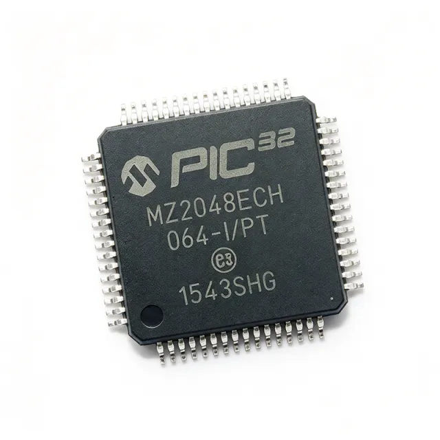
PIC32MZ2048ECH064-I/PT - 200MHz 2MB Flash 64-TQFP MCU | Microchip
Teilenummer: PIC32MZ2048ECH064-I/PT ✗ Abgekündigt| Menge | Stückpreis | Gesamt |
|---|---|---|
| 1 | $12.18 | $12,18 |
| 10 | $10.95 | $109,50 |
| 100 | $9.62 | $962,00 |
| 500 | $8.42 | $4.210,00 |
| 1.000 | $7.15 | $7.150,00 |
PIC32MZ2048ECH064-I/PT Übersicht
A 32-bit microcontroller (MCU) is a microprocessor-oriented integrated circuit that combines a high-performance CPU core, Flash program memory, SRAM data memory, and a wide range of on-chip peripherals such as ADCs, timers, communication interfaces, and DMA controllers on a single die. Within the broader taxonomy, PIC32MZ devices sit under MIPS M-Class microcontrollers -> 32-bit MCU -> microcontroller -> embedded processor -> semiconductor. The EC sub-family specifically adds high-bandwidth connectivity peripherals (HS USB, Ethernet, CAN) targeting industrial, IoT, and graphics/HMI use cases where wired connectivity is required.
Key features of the PIC32MZ2048ECH064-I/PT include 200 MHz core clock (with 252 MHz MIPS performance per DMIPS scaling), 2 MB dual-panel Flash supporting live update, 512 KB SRAM, integrated 10/100 Ethernet MAC with MII/RMII interface, HS USB 2.0 host/device/OTG, two CAN modules, multiple UART/SPI/I2C channels, a 12-bit ADC with up to 48 channels, and a hardware crypto engine. The device operates from 2.3V to 3.6V and supports an industrial -40C to +85C temperature range.
Architecturally, the PIC32MZ2048ECH064 uses the MIPS32 M-Class core with a 5-stage pipeline, hardware multiply/divide, DSP extensions, and a tightly coupled prefetch module that masks Flash latency at high clock rates. The 2 MB dual-panel Flash allows field firmware upgrades without halting the application, while 512 KB SRAM supports data buffering for graphics, audio, or networking stacks. Memory is accessed through a multi-beat eXternal Bus Interface (EBI) and a high-bandwidth RAM-on-chip bus to keep peripheral DMA fed.
Typical applications include industrial Ethernet gateways and PLCs, IoT edge nodes with TLS-secured cloud links, USB host/device peripherals, automotive infotainment subsystems, HMI panels with integrated graphics acceleration, and CAN-based motor control nodes. The wide connectivity set plus 2 MB Flash make it well-suited to applications running full TCP/IP stacks plus application code on a single chip.
When designing with this part, note that the 64-pin TQFP exposes only a subset of the 120+ pins available on larger variants - design the pinout early and verify Ethernet PHY, USB connector, and CAN transceiver wiring against the device's signal map. Decoupling follows the datasheet: 0.1 uF and 4.7 uF ceramic capacitors as close as possible to each power pin.
This page synthesizes the manufacturer datasheet (PIC32MZ EC Family Data Sheet, document 60001191G), distributor pricing from LCSC and Mouser, and a curated set of drop-in alternatives plus practical design notes not consolidated in the datasheet alone.
Drop-in-Alternativen für PIC32MZ2048ECH064-I/PT – gleiches Gehäuse, Pin-kompatibel. Bauteile mit anderem Gehäuse, die eine PCB-Überarbeitung erfordern, sind ausgeschlossen.
Varianten dieser Serie
Modelle derselben Serie, die drop-in-kompatibel sind mit PIC32MZ2048ECH064-I/PT (gleiche Bauform und Footprint) – abweichend in ADC, Package, USB, Core Architecture, CAN.
Schnellvergleichstool – Wählen Sie Alternativbauteile für den Direktvergleich:
PIC32MZ2048ECG064-I/PT
✓ Auf Lager
$17.42 / Stück
Datenblatt ansehen →PIC32MZ2048EFH064-I/PT
✓ Auf Lager
$8.55 / Stück
Datenblatt ansehen →PIC32MZ2048ECH100-I/PT
✓ Auf Lager
$11.75 / Stück
Datenblatt ansehen →PIC32MZ1024ECG064-I/PT
📋 Referenzalternative (nicht im Katalog)
PIC32MZ2048ECH064-I/PT Grenzwerte & elektrische Eigenschaften
| Core Architecture | MIPS32 M-Class (PIC32) |
| Maximum CPU Clock | 200 MHz |
| Performance | 252 DMIPS / 3.28 CoreMark/MHz |
| Program Flash | 2 MB (2048 KB) |
| SRAM | 512 KB |
| Operating Voltage | 2.3 V to 3.6 V |
| I/O Pins | 53 (64-pin TQFP) |
| Gehäuse | 64-pin TQFP (PT), 10x10 mm, 0.5 mm pitch |
| Temperature Range | -40 C to +85 C (Industrial) |
| Ethernet | 10/100 MAC with MII/RMII |
| USB | HS USB 2.0 Host/Device/OTG |
| CAN | 2x CAN 2.0B |
| ADC | 12-bit, up to 48 channels, 18 MSPS |
| Crypto Engine | AES, 3DES, SHA, MD5, RNG |
| DMA Channels | 32 (8 dedicated, 24 shared) |
| Timers | 9x 16-bit, 4x 32-bit |
| RoHS-Status | Compliant |
| MSL-Level | 3 |
PIC32MZ2048ECH064-I/PT Pin-Konfiguration
| Pin 1 | RP76/PMD15/SEG28/RTCC — Remappable I/O / Parallel Master Data / LCD Segment |
| Pin 2 | RP77/PMD14/SEG27 — Remappable I/O / Parallel Master Data / LCD Segment |
| Pin 3 | RP78/PMD13/SEG26 — Remappable I/O / Parallel Master Data / LCD Segment |
| Pin 4 | RP79/PMD12/SEG25 — Remappable I/O / Parallel Master Data / LCD Segment |
| Pin 5 | VDD — Digital supply voltage (3.3V nominal) |
| Pin 6 | RP80/PMD11/SEG24 — Remappable I/O / Parallel Master Data / LCD Segment |
| Pin 7 | RP81/PMD10/SEG23 — Remappable I/O / Parallel Master Data / LCD Segment |
| Pin 8 | RP82/PMD9/SEG22 — Remappable I/O / Parallel Master Data / LCD Segment |
| Pin 9 | RP83/PMD8/SEG21 — Remappable I/O / Parallel Master Data / LCD Segment |
| Pin 10 | VSS — Digital ground |
| Pin 11 | RP84/PMD7/SEG20 — Remappable I/O / Parallel Master Data / LCD Segment |
| Pin 12 | RP85/PMD6/SEG19 — Remappable I/O / Parallel Master Data / LCD Segment |
| Pin 13 | RP86/PMD5/SEG18 — Remappable I/O / Parallel Master Data / LCD Segment |
| Pin 14 | RP87/PMD4/SEG17 — Remappable I/O / Parallel Master Data / LCD Segment |
| Pin 15 | RP88/PMD3/SEG16 — Remappable I/O / Parallel Master Data / LCD Segment |
| Pin 16 | RP89/PMD2/SEG15 — Remappable I/O / Parallel Master Data / LCD Segment |
| Pin 17 | RP90/PMD1/SEG14 — Remappable I/O / Parallel Master Data / LCD Segment |
| Pin 18 | RP91/PMD0/SEG13 — Remappable I/O / Parallel Master Data / LCD Segment |
| Pin 19 | RP92/PMA22/SEG12 — Remappable I/O / Parallel Master Address / LCD Segment |
| Pin 20 | RP93/PMA21/SEG11 — Remappable I/O / Parallel Master Address / LCD Segment |
| Pin 21 | RP94/PMA20/SEG10 — Remappable I/O / Parallel Master Address / LCD Segment |
| Pin 22 | RP95/PMA19/SEG9 — Remappable I/O / Parallel Master Address / LCD Segment |
| Pin 23 | VDD — Digital supply voltage (3.3V nominal) |
| Pin 24 | VSS — Digital ground |
| Pin 25 | AERFD0/AETXD0/RPF0 — Ethernet MII/RMII TX/RX data 0 |
| Pin 26 | AERFD1/AETXD1/RPF1 — Ethernet MII/RMII TX/RX data 1 |
| Pin 27 | AERXERR/RPF2 — Ethernet MII RX error |
| Pin 28 | AECRS/RPF3 — Ethernet MII carrier sense |
| Pin 29 | AETXEN/RPF4 — Ethernet MII TX enable |
| Pin 30 | AERXDV/AECRS_DV/RPF5 — Ethernet MII/RMII RX valid / carrier sense |
| Pin 31 | AERXCLK/AEREF_CLK/RPF6 — Ethernet MII/RMII RX clock / reference clock |
| Pin 32 | AETXCLK/RPF7 — Ethernet MII TX clock |
| Pin 33 | AEMDIO/RPF8 — Ethernet MII management data |
| Pin 34 | AEMDC/RPF9 — Ethernet MII management clock |
| Pin 35 | VDD — Digital supply voltage (3.3V nominal) |
| Pin 36 | VSS — Digital ground |
| Pin 37 | RPF12/USBID — Remappable I/O / USB On-The-Go ID |
| Pin 38 | RPF13/USBVBUS — Remappable I/O / USB VBUS detect |
| Pin 39 | RP14/SDA3/U3CTS — Remappable I/O / I2C3 SDA / UART3 CTS |
| Pin 40 | RP15/SCL3/U3RTS — Remappable I/O / I2C3 SCL / UART3 RTS |
| Pin 41 | RP16/U4RX/C1TX — Remappable I/O / UART4 RX / CAN1 TX |
| Pin 42 | RP17/U4TX/C1RX — Remappable I/O / UART4 TX / CAN1 RX |
| Pin 43 | RP18/U5RX/C2TX — Remappable I/O / UART5 RX / CAN2 TX |
| Pin 44 | RP19/U5TX/C2RX — Remappable I/O / UART5 TX / CAN2 RX |
| Pin 45 | VDD — Digital supply voltage (3.3V nominal) |
| Pin 46 | VSS — Digital ground |
| Pin 47 | RP20/U1RTS/PMCS1 — Remappable I/O / UART1 RTS / Parallel Master Chip Select 1 |
| Pin 48 | RP21/U1CTS/PMCS2 — Remappable I/O / UART1 CTS / Parallel Master Chip Select 2 |
| Pin 49 | AN28/RP68/PMA8/U6TX — Analog input 28 / Remappable I/O / Parallel Master Address / UART6 TX |
| Pin 50 | AN29/RP69/PMA9/U6RX — Analog input 29 / Remappable I/O / Parallel Master Address / UART6 RX |
| Pin 51 | AN30/RP70/PMA10/U7TX — Analog input 30 / Remappable I/O / Parallel Master Address / UART7 TX |
| Pin 52 | AN31/RP71/PMA11/U7RX — Analog input 31 / Remappable I/O / Parallel Master Address / UART7 RX |
| Pin 53 | RP22/PMA0/U2CTS — Remappable I/O / Parallel Master Address / UART2 CTS |
| Pin 54 | RP23/PMA1/U2RTS — Remappable I/O / Parallel Master Address / UART2 RTS |
| Pin 55 | RP24/PMA2/U3TX — Remappable I/O / Parallel Master Address / UART3 TX |
| Pin 56 | RP25/PMA3/U3RX — Remappable I/O / Parallel Master Address / UART3 RX |
| Pin 57 | RP26/PMA4/U4TX — Remappable I/O / Parallel Master Address / UART4 TX |
| Pin 58 | RP27/PMA5/U4RX — Remappable I/O / Parallel Master Address / UART4 RX |
| Pin 59 | AVDD — Analog supply voltage |
| Pin 60 | AVSS — Analog ground |
| Pin 61 | OSC1/CLKI/RPA15 — Crystal oscillator input / external clock |
| Pin 62 | OSC2/CLKO/RPA14 — Crystal oscillator output / system clock output |
| Pin 63 | MCLR — Master clear / reset input (active low) |
| Pin 64 | PGED2/RPG6 — Programming data line 2 / Remappable I/O |
Typische Anwendungen
PIC32MZ2048ECH064-I/PT ist geeignet für 7 Anwendungs: Industrial Ethernet Gateway, USB Host/Device Peripheral, CAN-Based Motor Control Node, IoT Edge Node with TLS Security, Automotive Infotainment Subsystem, HMI Panel with Touch Interface, Audio Processing Embedded System.
Industrial Ethernet Gateway
The PIC32MZ2048ECH064-I/PT's integrated 10/100 Ethernet MAC with MII/RMII interface and 2 MB Flash make it ideal for industrial Ethernet gateways and protocol converters that bridge Modbus TCP, EtherNet/IP, or PROFINET fieldbuses. The 200 MHz MIPS core runs full TCP/IP stacks plus application logic, while the 512 KB SRAM buffers incoming packets without dropping frames. Pair the MCU with an external PHY like the KSZ8081 for the physical layer; the ECH variant's 53 I/O pins provide ample headroom for RS-485, SPI sensor, and UART expansion. Industrial temperature rating to +85C supports factory-floor deployment. Power dissipation at 200 MHz is approximately 240 mW with all peripherals active - well within the TQFP-64 thermal budget for closed enclosures. Estimated: 3.3V x 73 mA typical core current per the datasheet DC characteristics.
Empfohlen
USB Host/Device Peripheral
The PIC32MZ2048ECH064-I/PT integrates HS USB 2.0 host/device/OTG with on-chip transceivers, enabling USB peripherals like data loggers, mass storage devices, or HID controllers without an external ULPI PHY. The 200 MHz core supports USB stack processing at high bus bandwidth, and 512 KB SRAM buffers bulk transfers to USB flash drives or printers. The MCU's DMA channels offload endpoint transfers from the CPU, sustaining throughput while leaving headroom for application code. The 2 MB Flash stores USB class drivers and bootloader plus user application; dual-panel Flash enables field firmware updates over USB. Industrial-grade -40C to +85C operation suits instrumentation and POS terminals. Estimated: HS USB host current ~120 mA additional, requiring the VBUS pin protection circuit per datasheet USB section.
Empfohlen
CAN-Based Motor Control Node
The PIC32MZ2048ECH064-I/PT's dual CAN 2.0B controllers with hardware acceptance filters make it suitable for distributed motor control nodes communicating over CANopen or CAN-FD networks. The 200 MHz core with DSP extensions runs field-oriented control (FOC) algorithms at 20 kHz PWM rates with comfortable margin for CAN stack and safety logic. The 12-bit ADC with 48 channels and 18 MSPS samples three-phase current and voltage simultaneously, while DMA streams samples to SRAM without CPU intervention. The 2 MB Flash fits motor-control libraries plus CANopen stack, and 512 KB SRAM accommodates look-up tables and observer state. Use a CAN transceiver like the MCP2561FD between the MCU and the bus. The 64-TQFP's 53 I/O expose PWM outputs, encoder inputs, and auxiliary GPIOs for end-of-line and STO safety signals. Estimated: FOC loop at 20 kHz consumes ~30% CPU with 200 MHz clock per typical application notes.
Empfohlen
IoT Edge Node with TLS Security
The PIC32MZ2048ECH064-I/PT's hardware crypto engine (AES, 3DES, SHA, MD5, RNG) and 2 MB Flash make it ideal for IoT edge nodes performing TLS handshakes and encrypted MQTT/HTTPS communication over Ethernet or Wi-Fi. The crypto engine offloads AES-128/256 from the CPU, sustaining TLS throughput while leaving the MIPS core free for sensor aggregation and edge analytics. The 512 KB SRAM fits TLS session buffers plus FreeRTOS or Harmony stacks. Pair with a Wi-Fi module like the ATWINC1500 for wireless variants, or use the integrated Ethernet MAC for wired IoT. Industrial temperature rating and 200 MHz performance handle local decision-making before cloud upload. Power consumption scales with peripheral use; with crypto engine active expect ~280 mW at full load. Estimated: 3.3V x 85 mA combined core plus peripherals per datasheet typical values.
Empfohlen
Automotive Infotainment Subsystem
The PIC32MZ2048ECH064-I/PT's USB host/device, Ethernet, CAN, and graphics peripherals support automotive infotainment subsystems like head-unit controllers, telematics modules, and rear-seat entertainment HMI. The 200 MHz core with graphics-friendly peripherals drives small TFT displays up to WVGA via the parallel memory interface, while CAN interfaces with vehicle body networks. The 2 MB Flash holds graphics assets and audio codecs, and 512 KB SRAM serves as frame buffer for partial-screen updates. The device supports automotive temperature grades when ordered as the -V variant (-40C to +105C); the industrial -I variant serves cabin electronics and aftermarket accessories. The 64-TQFP footprint suits compact PCBAs behind radio bezels. Estimated: graphics + USB + CAN active draws ~310 mW at 3.3V per application note typical-power figures.
Empfohlen
HMI Panel with Touch Interface
The PIC32MZ2048ECH064-I/PT's 200 MHz core, 53 I/O pins, and parallel graphics interface enable HMI panels for industrial machines, building automation, and medical device user interfaces. The 12-bit ADC integrates with resistive touch-sensing circuitry for touch input, or pair with an external capacitive touch controller via I2C/SPI for higher-touch-count screens. The 2 MB Flash stores multi-language UI assets and configuration data, and 512 KB SRAM buffers graphics pages and animation frames. DMA channels accelerate display refresh without CPU intervention, keeping the MIPS core available for protocol handling. Industrial -40C to +85C temperature rating supports factory and outdoor enclosures. The crypto engine secures OTA firmware updates. Estimated: graphics refresh + touch scan consumes ~260 mW typical at full display update rate.
Empfohlen
Audio Processing Embedded System
The PIC32MZ2048ECH064-I/PT's 200 MHz MIPS core with DSP extensions, 512 KB SRAM, and I2S-compatible peripherals support audio processing embedded systems like professional mixers, instrument tuners, and effects pedals. The DSP extensions accelerate FFT, FIR, and IIR filters for real-time audio manipulation, while 512 KB SRAM buffers multiple audio channels at 48 kHz sample rates without dropping samples. The I2S peripheral interfaces with audio DACs and ADCs, and the dual CAN or Ethernet ports enable networked audio distribution in installations. The 2 MB Flash stores presets, DSP algorithm parameters, and USB MIDI class firmware. Industrial temperature rating supports touring equipment. Estimated: 16-channel 48 kHz processing consumes ~70% of CPU; add the FPU variant for higher channel counts.
Empfohlen
Zusammenfassung der empfohlenen Produkte
Technische Referenzdaten für PIC32MZ2048ECH064-I/PT – Vergleich, Designhinweise und Compliance-Informationen.
Auswahlhilfe
Vergleich mit Alternativen
| Parameter | Dieses Produkt | PIC32MZ2048ECG064-I/PT | PIC32MZ1024ECG064-I/PT | PIC32MZ2048EFH064-I/PT |
|---|---|---|---|---|
| Package | 64-TQFP (PT, 10x10 mm) | 64-TQFP (PT, 10x10 mm) - same | 64-TQFP (PT, 10x10 mm) - same | 64-TQFP (PT, 10x10 mm) - same |
| Brand | Microchip Technology | Microchip Technology | Microchip Technology | Microchip Technology |
| Core Clock | 200 MHz | 200 MHz | 200 MHz | 252 MHz |
| Program Flash | 2 MB | 2 MB | 1 MB | 2 MB |
| SRAM | 512 KB | 512 KB | 256 KB | 512 KB |
| FPU | No | No | No | Yes (IEEE 754 single-precision) |
| Ethernet MAC | Yes (10/100 MII/RMII) | No | No | Yes (10/100 MII/RMII) |
| USB | HS USB 2.0 Host/Device/OTG | HS USB 2.0 Host/Device/OTG | HS USB 2.0 Host/Device/OTG | HS USB 2.0 Host/Device/OTG |
| Lifecycle Status | NRND (EOL Jan 2027) | Active | Active | Active |
Wichtigste Unterscheidungsmerkmale
- Integrated 10/100 Ethernet MAC on the EC variant (vs. PIC32MZ2048ECG064-I/PT)
- Recommended FPU-enabled successor with same package (vs. PIC32MZ2048EFH064-I/PT)
- 2 MB Flash vs 1 MB on the lower-memory variant (vs. PIC32MZ1024ECG064-I/PT)
Designhinweise
Per the PIC32MZ EC family datasheet (60001191G), place a 0.1 uF ceramic decoupling capacitor within 3 mm of every VDD pin and a 4.7 uF bulk capacitor on each main 3.3V rail. The AVDD analog supply requires a 0.1 uF plus 10 uF pair with a ferrite bead isolating it from digital supply noise. The PLL supply VDDPLL needs a dedicated filter network (resistor and capacitor) within 5 mm of the pin to minimize jitter. Avoid routing high-frequency digital signals near AVDD to prevent ADC noise injection.
At 200 MHz with all peripherals active, the PIC32MZ2048ECH064-I/PT draws approximately 70-85 mA from the 3.3V supply, dissipating roughly 240-280 mW. Estimated: 3.3V x 80 mA typical current per the datasheet DC characteristics section. The TQFP-64 package has a theta_JA of approximately 40 C/W on a standard 4-layer JEDEC test board, giving a junction temperature rise of about 11 C at 280 mW. Industrial temperature range to +85C is achievable without active cooling for typical industrial enclosures. Verify thermal performance with the actual PCB layout using the Microchip thermal model.
Route the USB DP and DM lines as a 90-ohm differential pair with continuous reference plane on the layer below. Keep the pair length-matched within 150 mil per USB 2.0 high-speed requirements and avoid stubs. The Ethernet MII/RMII signals to the external PHY should be length-matched within 500 mil and routed over a continuous ground plane. Place the 24 MHz crystal within 5 mm of the OSC1/OSC2 pins with short traces and a ground guard ring to minimize EMI. Use impedance-controlled 50-ohm routing for the USB and Ethernet signals with the appropriate stack-up.
Do not enable the 200 MHz core clock without first configuring the PLL and wait states correctly - the Flash access time requires wait states at high clock rates. Always configure the prefetch cache and write buffer settings as specified in the PIC32MZ EC family reference manual. When migrating firmware between EC and EF family parts, verify peripheral library paths - the EC and EF register names differ in several places, particularly around the FPU integration in the EF family.
The dual-panel Flash architecture allows live firmware updates, but requires careful linker script configuration to map the active panel correctly during boot. Use the Microchip Harmony configuration tool or the MPLAB XC32 linker scripts to set the upper and lower Flash panel boundaries. During live update, disable interrupts that could trigger Flash erase operations on the inactive panel to prevent corruption. The 512 KB SRAM is divided into separate bus matrix regions; verify DMA channel mappings to avoid bus contention.
Compliance-Informationen
RoHS and REACH compliant per Microchip product page; Pb-free TQFP package; MSL Level 3 per JEDEC J-STD-020. Not AEC-Q100 qualified for automotive - choose -V variant for AEC-Q100 grade.


