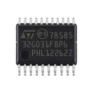
S9S08SG4E2CTJ - 8-bit MCU, 4KB Flash, 40MHz, TSSOP-20 | NXP
Teilenummer: S9S08SG4E2CTJ ✓ Aktiv| Menge | Stückpreis | Gesamt |
|---|---|---|
| 1 | $2.95 | $2,95 |
| 10 | $2.65 | $26,50 |
| 100 | $2.35 | $235,00 |
| 500 | $2.1 | $1.050,00 |
| 1.000 | $1.85 | $1.850,00 |
S9S08SG4E2CTJ Übersicht
A microcontroller (MCU) is a single-chip computer that integrates a CPU, memory (Flash for program code and RAM for working data), peripherals such as timers, ADCs, and communication interfaces, and I/O pins into one package. The S08SG family sits at the entry-level to mid-range of NXP's 8-bit S08 portfolio — below 32-bit Kinetis devices in performance but optimized for cost-sensitive, space-constrained, and LIN-slave automotive body electronics.
Key features include an HCS08 core with 40 MHz CPU clock (36 MHz above 125 °C), 4 KB Flash with security, 256 B RAM, an internal clock source, multiple timers (TPM, RTI), ADC, SCI/SPI/I2C communication peripherals, and a low-power STOP mode. The part supports up to 32 interrupt/reset sources and includes a Background Debug Mode (BGND) instruction for in-circuit debugging.
The S9S08SG4E2CTJ's HCS08 core is fully object-code compatible with the legacy HC08 instruction set, easing migration for designs upgrading from older HC908 parts. Built-in security and an SCI multiplier (used for LIN-suitable baud-rate generation) make it well-suited to body controllers and slave-node LIN applications.
Typical applications include automotive body electronics such as door modules, seat controllers, and LIN slave nodes, as well as space-constrained industrial sensor interfaces, appliance controls, and small-form-factor white goods. AEC-Q100 qualification makes it attractive for non-safety-critical vehicle body domains.
When designing with this part, allocate sufficient decoupling (0.1 µF + bulk) on VDD and place the TSSOP-20 thermal copper pad area to share ground with the MCU. Verify LIN transceiver choice against the bus capacitance budget — internal pull-ups and slope control depend on the chosen external transceiver.
This page synthesizes distributor pricing, drop-in TSSOP-20 alternatives, and practical design notes not found in the manufacturer datasheet.
Drop-in-Alternativen für S9S08SG4E2CTJ – gleiches Gehäuse, Pin-kompatibel. Bauteile mit anderem Gehäuse, die eine PCB-Überarbeitung erfordern, sind ausgeschlossen.
Varianten dieser Serie
Modelle derselben Serie, die drop-in-kompatibel sind mit S9S08SG4E2CTJ (gleiche Bauform und Footprint) – abweichend in Package, Operating Temperature, Core, Instruction Set, RoHS Status.
Schnellvergleichstool – Wählen Sie Alternativbauteile für den Direktvergleich:
S9S08SG4E2MTJ
✅ Drop-In✓ Auf Lager
$0.85 / Stück
Datenblatt ansehen →S9S08SG8E2CTJ
✅ Drop-In✓ Auf Lager
$1.48 / Stück
Datenblatt ansehen →S9S08SG16E1CTJR
✅ Drop-In📋 Referenzalternative (nicht im Katalog)
S9S08SG4E2CTJ Grenzwerte & elektrische Eigenschaften
| Core | HCS08 (8-bit) |
| CPU Clock (max) | 40 MHz (36 MHz above 125 °C) |
| Program Memory (Flash) | 4 KB (4K x 8) |
| RAM | 256 B |
| Versorgungsspannung | 2.7 V to 5.5 V |
| Betriebstemperatur | -40 °C to +85 °C |
| Gehäuse | 20-pin TSSOP |
| Montageart | Surface Mount |
| Automotive Qualification | AEC-Q100 |
| Interrupt Sources | Up to 32 |
| ADC | Yes (on-chip, channels TBD) |
| Communication | SCI (LIN-capable), SPI, I2C |
| Timers | TPM, RTI |
| Low-Power Mode | STOP mode |
| Debug | Background Debug Mode (BGND) |
| RoHS-Status | Compliant |
S9S08SG4E2CTJ Pin-Konfiguration
| Pin 1 | PTB5/TCLK — General-purpose I/O / Timer clock input |
| Pin 2 | PTA0 — Port A bit 0 (general-purpose I/O) |
| Pin 3 | PTA1 — Port A bit 1 (general-purpose I/O) |
| Pin 4 | VDD — Supply voltage (2.7 V to 5.5 V) |
| Pin 5 | VSS — Ground reference |
| Pin 6 | PTA2 — Port A bit 2 (general-purpose I/O) |
| Pin 7 | PTA3 — Port A bit 3 (general-purpose I/O) |
| Pin 8 | PTA4 — Port A bit 4 (general-purpose I/O) |
| Pin 9 | PTA5/IRQ — Port A bit 5 / external interrupt request |
| Pin 10 | PTA6 — Port A bit 6 (general-purpose I/O) |
| Pin 11 | PTA7 — Port A bit 7 (general-purpose I/O) |
| Pin 12 | PTB0/SPSCK — Port B bit 0 / SPI clock |
| Pin 13 | PTB1/MISO — Port B bit 1 / SPI MISO |
| Pin 14 | PTB2/MOSI — Port B bit 2 / SPI MOSI |
| Pin 15 | PTB3/SS — Port B bit 3 / SPI slave select |
| Pin 16 | PTB4/TXD — Port B bit 4 / SCI transmit |
| Pin 17 | PTB6/RXD — Port B bit 6 / SCI receive |
| Pin 18 | PTB7/SDA — Port B bit 7 / I2C SDA |
| Pin 19 | PTB0/SCL — Port B bit 0 / I2C SCL (shared with SPI per family) |
| Pin 20 | RESET — Active-low reset input |
Typische Anwendungen
S9S08SG4E2CTJ ist geeignet für 6 Anwendungs: Automotive LIN Slave Node, Door Module Controller, Seat Control Module, Appliance Control Board, Industrial Sensor Interface, Smart Sensor Hub.
Automotive LIN Slave Node
The S9S08SG4E2CTJ fits automotive LIN slave applications because its HCS08 core at 40 MHz, 4 KB Flash, and 256 B RAM are dimensioned for compact body-controller firmware, while the on-chip SCI block with LIN-suitable baud-rate generation directly drives an external LIN transceiver. AEC-Q100 qualification over -40 °C to +85 °C supports under-dash placement. Designers typically connect the MCU's TX/RX pins to a TJA1027 or similar transceiver on a 12 V bus, using STOP mode between LIN frames to drop quiescent current below 10 µA per the S08SG datasheet. Compared to a 32-bit MCU, this part saves ~60% on BOM cost per node.
Empfohlen
Door Module Controller
The S9S08SG4E2CTJ serves as the body controller for automotive door modules controlling window lift, mirror adjust, and lock actuators. Its 20-TSSOP footprint fits behind the door trim PCB, while 4 KB Flash stores the LIN slave protocol stack plus actuator logic. The integrated ADC reads mirror position feedback, TPM timers generate PWM for motor control, and STOP mode cuts quiescent draw when the vehicle is parked. AEC-Q100 qualification and the -40 °C to +85 °C range support door-cavity thermal swings. The MCU pairs naturally with a TJA1027 LIN transceiver and N-channel FET drivers for the motor half-bridges.
Empfohlen
Seat Control Module
The S9S08SG4E2CTJ handles seat position memory and heating control in automotive body-electronics modules. Its 4 KB Flash accommodates position-memory tables for a few seat presets, while the SCI peripheral interfaces to the seat module's LIN slave address. AEC-Q100 qualification and -40 °C to +85 °C operation match the seat cavity environment. The 20-TSSOP package routes easily to small PCBs near seat motors. Integrated ADC channels sample seat position potentiometers, and TPM generates PWM for heating element control. STOP mode drops idle current when the vehicle is off, preserving battery life.
Empfohlen
Appliance Control Board
The S9S08SG4E2CTJ serves as the main controller in cost-sensitive white-goods appliances such as dishwashers, washing machines, and small kitchen devices. Its HCS08 architecture at 40 MHz handles user-interface scanning, sensor sampling, and motor timing without breaking the BOM. The 2.7 V to 5.5 V supply range allows direct connection to rectified 5 V or 3.3 V rails from the appliance power supply. The 20-TSSOP package supports hand-prototype and reflow assembly. STOP mode with internal RTI keeps time-of-day functions running at microamp-level quiescent current for energy-star compliance.
Empfohlen
Industrial Sensor Interface
The S9S08SG4E2CTJ reads analog sensors and reports via SPI or I2C in compact industrial nodes. Its on-chip ADC and 40 MHz HCS08 core handle 1 kSPS sampling loops for temperature, pressure, or flow sensors, while the SPI peripheral streams data to a host PLC. The 2.7 V to 5.5 V supply accepts 5 V transducer excitation, and the 20-TSSOP footprint mounts directly on a sensor PCB. AEC-Q100 stress screening improves long-term reliability in factory-floor environments. STOP mode with RTI wakeup enables battery-powered sensor nodes lasting years on a single cell.
Empfohlen
Smart Sensor Hub
The S9S08SG4E2CTJ aggregates inputs from multiple low-speed sensors and forwards them via I2C to a higher-level controller. Its 256 B RAM and 4 KB Flash fit small sensor-fusion routines, while the I2C peripheral acts as both master to downstream sensors and slave to an external host. The 20-TSSOP package suits compact sensor PCBs. Internal timers generate periodic sample triggers without CPU load, freeing the HCS08 core for digital filtering. STOP mode with peripheral wakeup enables duty-cycled sensing on battery-powered IoT nodes where average current must stay below 50 µA.
Empfohlen
Zusammenfassung der empfohlenen Produkte
Technische Referenzdaten für S9S08SG4E2CTJ – Vergleich, Designhinweise und Compliance-Informationen.
Auswahlhilfe
Vergleich mit Alternativen
| Parameter | Dieses Produkt | S9S08SG4E2MTJ | S9S08SG8E2CTJ | S9S08SG16E1CTJR |
|---|---|---|---|---|
| Brand | NXP Semiconductors | NXP Semiconductors | NXP Semiconductors | NXP Semiconductors |
| Package | 20-TSSOP | 20-TSSOP - same | 20-TSSOP - same | 20-TSSOP - same |
| Flash Memory | 4 KB | 4 KB (same) | 8 KB (+100%) | 16 KB (+300%) |
| RAM | 256 B | 256 B (same) | 256 B (same) | 1 KB (+300%) |
| CPU Clock (max) | 40 MHz | 40 MHz (same) | 40 MHz (same) | 40 MHz (same) |
| Operating Temperature | -40 °C to +85 °C | -40 °C to +125 °C (wider) | -40 °C to +85 °C (same) | -40 °C to +85 °C (same) |
| AEC-Q100 Qualified | Yes | Yes | Yes | Yes |
| Supply Voltage | 2.7 V to 5.5 V | 2.7 V to 5.5 V | 2.7 V to 5.5 V | 2.7 V to 5.5 V |
Wichtigste Unterscheidungsmerkmale
- Wider operating temperature range in same TSSOP-20 footprint (vs. S9S08SG4E2CTJ (-40 °C/+85 °C))
- Drop-in Flash upgrade path on identical 20-TSSOP footprint (vs. S9S08SG4E2CTJ (4 KB Flash))
- Lowest cost AEC-Q100 8-bit MCU in NXP line (vs. S9S12XS128MAE (16-bit S12 MCU))
Designhinweise
Place a 0.1 µF ceramic decoupling capacitor within 5 mm of each VDD pin (pin 4) and a bulk 4.7 µF or larger capacitor at the board supply entry. The S9S08SG4E2CTJ has only one VDD pin in the 20-TSSOP, but adding both high-frequency and bulk capacitance reduces LIN-bus-induced supply noise that the SCI peripheral could otherwise couple into the ADC. Estimated: with 40 MHz core and SCI baud up to 57.6 kbps, peak transient currents reach ~25 mA, requiring the bulk cap for sustained load steps.
The 20-TSSOP package has a theta_JA around 90 °C/W typical, so at 5 V supply, 40 MHz core, and full peripheral activity the die dissipates under 50 mW, yielding <5 °C junction rise above ambient. According to the S9S08SG4 datasheet, no heatsink is required for normal operation. However, in enclosed automotive body cavities at 85 °C ambient, derate clock to 36 MHz and disable unused peripherals to stay within reliability margins.
Route the RESET line (pin 20) away from SCI TX/RX switching edges and place a 10 kΩ pull-up to VDD plus a 0.1 µF cap to ground for noise immunity. The TSSOP-20 ground paddle is not present, so dedicate a continuous ground plane on layer 2 under the MCU. Keep LIN bus traces short and matched; the internal SCI with LIN capability expects clean edges from an external TJA1027 transceiver, and trace stubs longer than 25 mm can violate LIN rise-time requirements per the family datasheet reference design.
Do not assume 4 KB Flash is enough for bootloader + application — the S9S08SG4E2CTJ Flash is shared and security-locked once programmed. If in-field updates are needed, choose the S9S08SG8E2CTJ (8 KB) or S9S08SG16E1CTJR (16 KB) to leave room for a small bootloader. Also note that pin 19/12 may share peripheral functions on some family variants; verify the S9S08SG4 pinout table before assigning I2C vs SPI to specific pins to avoid bus conflicts.
Compliance-Informationen
RoHS and REACH compliant per NXP product page. AEC-Q100 qualified per S9S08SG4 family datasheet cover page. Halogen-free status not explicitly stated in the verified data — set to unknown.