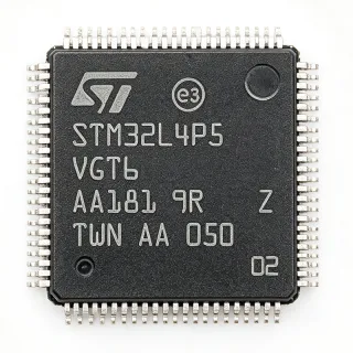
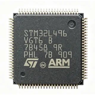
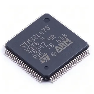
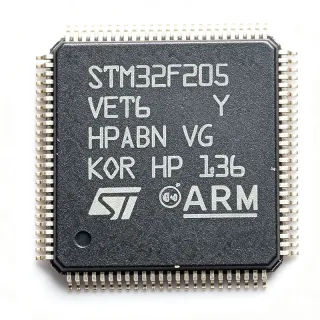
STM32F103VGT7 - 72MHz Cortex-M3 MCU 1MB Flash 100-LQFP | ST
Teilenummer: STM32F103VGT7 ✓ Aktiv| Menge | Stückpreis | Gesamt |
|---|---|---|
| 1 | $13.62 | $13,62 |
| 10 | $12.1 | $121,00 |
| 100 | $10.45 | $1.045,00 |
| 500 | $9.3 | $4.650,00 |
| 1.000 | $8.6 | $8.600,00 |
STM32F103VGT7 Übersicht
A microcontroller (MCU) is a single-chip computer that integrates a CPU core, memory and programmable I/O peripherals onto one die. Within the broader IC taxonomy, an MCU belongs to the microprocessor IC family, which sits above microcontrollers but below microprocessors in computational capability. The Cortex-M3 core inside this STM32 belongs to ARM's Cortex-M profile, designed for deterministic real-time embedded workloads; the Cortex-M3 line is one rung below Cortex-M4 in DSP capability and one rung above Cortex-M0+ in raw compute throughput.
Key features of the STM32F103VGT7 include a 72 MHz maximum CPU clock with single-cycle multiply, two 12-bit ADCs (1 µs conversion), seven general-purpose 16-bit timers plus one PWM timer for motor control, three USARTs, two UARTs, two SPIs and one I2C, an FS-USB device, a CAN 2.0B interface, an SDIO interface, an FSMC for external memory, 80 GPIO lines and a -40 °C to +105 °C operating range. The XL-density die provides the largest Flash and SRAM footprint of the STM32F1 series, enabling sophisticated firmware with rich connectivity stacks.
The architecture pairs a Harvard-bus Cortex-M3 with a multi-AHB bus matrix that lets CPU, DMA and peripherals operate concurrently with deterministic bus latency. The 72 MHz core drives a 1.25 DMIPS/MHz figure (1.25 DMIPS/MHz), yielding 90 DMIPS total performance. The chip supports JTAG and SWD debug, an embedded Cortex-M3 trace macrocell (ETM), and boundary-scan for production test.
Typical uses include motor drives (BLDC, stepper), USB HID/COM bridges, industrial PLCs, CNC controllers, CNC and 3D-printer mainboards, data-acquisition modules, CAN-bus nodes, RFID readers and point-of-sale terminals. Designers favor the part for its mature firmware ecosystem (HAL, LL, StdPeriph), reference schematics and broad ST Nucleo board support.
When laying out, place the VDD/VSS/VBAT/VDDA pins with 100 nF decoupling within 3 mm of each power pin, plus a 1 µF bulk on VDDA; keep the HSE crystal traces short and guarded to avoid EMI on USB. Make sure the BOOT0 strap on the part is hardware-defaulted for Flash boot when designing for field upgrades. This page consolidates distributor pricing (as of 2026-10-21), pin-to-pin same-brand and cross-brand drop-in alternatives (GD32F103 series) and practical design notes not found in the manufacturer datasheet.
Drop-in-Alternativen für STM32F103VGT7 – gleiches Gehäuse, Pin-kompatibel. Bauteile mit anderem Gehäuse, die eine PCB-Überarbeitung erfordern, sind ausgeschlossen.
Varianten dieser Serie
Modelle derselben Serie, die drop-in-kompatibel sind mit STM32F103VGT7 (gleiche Bauform und Footprint) – abweichend in Package, Mounting Type, RoHS Status, ADC, Core Architecture.
Schnellvergleichstool – Wählen Sie Alternativbauteile für den Direktvergleich:
STM32F103VGT6
✅ Drop-In📋 Referenzalternative (nicht im Katalog)
STM32F103VFT6
✅ Drop-In📋 Referenzalternative (nicht im Katalog)
STM32F103VDT7
✅ Drop-In📋 Referenzalternative (nicht im Katalog)
GD32F103VGT7
✅ Drop-In📋 Referenzalternative (nicht im Katalog)
GD32F103VFT6
✅ Drop-In📋 Referenzalternative (nicht im Katalog)
APM32F103VGT7
✅ Drop-In📋 Referenzalternative (nicht im Katalog)
STM32F103VGT7 Grenzwerte & elektrische Eigenschaften
| Core | ARM Cortex-M3 |
| Core Architecture | 32-bit RISC, Harvard bus |
| Maximum CPU Clock | 72 MHz |
| Performance | 1.25 DMIPS/MHz (90 DMIPS) |
| Program Memory | 1 MB Flash |
| SRAM | 96 KB |
| Gehäuse | 100-LQFP (14x14 mm) |
| Montageart | Surface Mount |
| Operating Voltage | 2.0 V to 3.6 V |
| Betriebstemperatur | -40 C to +105 C |
| GPIO Count | 80 |
| ADC | 2x 12-bit, up to 16 channels, 1 MSPS |
| Timers | 7x 16-bit + 1x PWM (motor control) |
| Communication | USB FS, 2x CAN 2.0B, 3x USART, 2x UART, 3x SPI, 2x I2S, 2x I2C, SDIO, FSMC |
| Debug Interface | JTAG + SWD + ETM |
| RoHS-Status | Compliant |
STM32F103VGT7 100-lqfp (14x14 mm) Pinbelegungsleitfaden
Pinbelegung für STM32F103VGT7 (100-lqfp (14x14 mm)-Gehäuse). Dieser digitale IC umfasst GPIO, Kommunikationsschnittstellen (UART, SPI, I2C) und Versorgungspins. Alternative Pin-Funktionen und Konfigurationsoptionen entnehmen Sie dem Herstellerdatenblatt. Unverzichtbar für Embedded-System-Design und PCB-Layout.

Keine detaillierten Pinbelegungsdaten verfügbar für STM32F103VGT7.
Siehe die Datenblatt für die vollständige Pin-Konfiguration.
Typische Anwendungen
STM32F103VGT7 ist geeignet für 7 Anwendungs: Brushless DC Motor Drives, USB HID / COM Bridge Devices, Industrial CAN-bus Nodes, Cobot and Industrial PLC Hubs, 3D Printer and CNC Control Boards, Medical Data-Acquisition Modules, Point-of-Sale and Vending Terminals.
Brushless DC Motor Drives
The STM32F103VGT7 is a strong fit for BLDC and PMSM motor drives thanks to its 1 MSPS 12-bit ADC (dual ADC support for current-sense capture), one advanced PWM timer (TIM1) capable of complementary outputs with programmable dead-time, and the 72 MHz Cortex-M3 running deterministic FOC loops at 16 kHz without overload. The 1 MB Flash holds application firmware plus ST motor-control workbench libraries, and 96 KB SRAM keeps current-control buffers and observer state local for low-latency execution. The chip's CAN interface shares the PA11/PA12 bus (or PB5/PB6) with USB or other buses for CANopen integration, enabling the IC to drive 36 V/2 kW tools or e-bike hubs across multi-axis systems.
Empfohlen
USB HID / COM Bridge Devices
With an integrated USB 2.0 full-speed device controller and on-chip PHY, the STM32F103VGT7 needs no external transceiver to act as a USB HID, CDC/VCP, DFU bootloader or vendor-class bridge. PA11/PA12 double as DP/DM, and 80 GPIO plus dual ADC channels let a single IC replace an external MCU+USB controller two-chip solution. Compared with smaller-density STM32F103 parts, the VGT7 has plenty of Flash for composite USB stacks (HID + CDC + vendor) plus user firmware, often making it the lowest-cost solution. Pair the design with an external EEPROM for device-serial storage and a 12 MHz HSE crystal for full USB-IF compliance.
Empfohlen
Industrial CAN-bus Nodes
The STM32F103VGT7's two bxCAN 2.0B interfaces (each with 14 filter banks and 1 Mbit/s capability) make it ideal for industrial CANopen and DeviceNet slave nodes, sensor clusters and PLC I/O modules. It withstands 105 °C ambient die temperature and integrates both an FSMC bus (for external SRAM/Flash extension) and a 1 MSPS ADC for analog backplanes, removing the need for a companion MCU. Dual bxCAN also enables CAN-bus bridge / repeater / router designs, or CAN-to-UART gateways in substation automation. Use the ST's CANopen slave stack or PEAK-System PCAN libraries; CAN tranceiver TJA1050 or TJA1051T isolates the MCU from physical bus faults.
Empfohlen
Cobot and Industrial PLC Hubs
The combination of 1 MB Flash (room for IEC 61131-3 runtime + safety scaffolding), 96 KB SRAM (PLC ladder logic + retentive tags), 80 GPIO, and a 12-bit ADC qualifies the STM32F103VGT7 as a 100-MHz-class PLC main processor for cobot controllers and industrial hubs. The on-chip FSMC bus permits off-die SRAM/PSRAM extension up to 16 MB for HMI buffers and PID-loop workspaces; dual ADC supports redundant analog-input sampling; the USB and CAN interfaces connect to sensor and HMI panels. Although not AEC-Q100, the industrial -40/+105 C die temperature of the VGT7 grade suffices for cabinet-mounted controls.
Empfohlen
3D Printer and CNC Control Boards
The STM32F103VGT7's PWM timer + 1 MSPS ADC pair stepper or DC-servo control well for low-end 3D printers and CNC controllers (later revisions favor STM32F407/F411 for FPU+USB-HS). The XL-density 1 MB Flash holds Marlin/Smoothieware firmware plus user-tunable G-code optimizations; 96 KB SRAM keeps look-ahead queues and step-pulse scheduling in real time. SDIO + SPI expose SD-card interfaces for G-code files, while USB-VCP enables drop-in host wiring to PCs running Pronterface or OctoPrint. Should the application grow beyond G-code handling or need a USB-HS PHY or larger Flash, upgrade to STM32F407VGT6 in the same LQFP-100 footprint.
Empfohlen
Medical Data-Acquisition Modules
Although not AEC-Q100, the STM32F103VGT7's analog performance (dual 12-bit 1 MSPS ADC with separate VDDA), 1 MB Flash, and deterministic Cortex-M3 cores qualify it for non-invasive medical data-acquisition designs (e.g., SpO2, ECG front-ends, pulse-oximeter engines). The FSMC bus enables an external SRAM or graphics-LCD display driver. Designers add a low-side AFE like AD8232 with separate isolated power; total BOM is substantially smaller than a discrete MCU+ASIC pair. For FDA-cleared designs, engineers typically migrate to the STM32F4 family (FPU for DSP) or the STM32H7 line, but the F103VG remains common in OEM prototyping.
Empfohlen
Point-of-Sale and Vending Terminals
POS terminals and unattended kiosks use the STM32F103VGT7 as a low-power Cortex-M3 main controller handling barcode readers, NFC/RFID, thermal printers, and external GPRS or Ethernet modules over UART/SPI/USB. The large Flash holds firmware for printer control, MDB (Multi-Drop Bus) peripherals, and a small embedded web-server; the on-chip CAN and FSMC expand into multi-drop beverage vending. Its 100-LQFP footprint provides abundant GPIO for keypad scanning, LCD module interfacing, and relay switching, and dual ADC channels sample battery voltage and thermistor networks for unattended-system reliability.
Empfohlen
Zusammenfassung der empfohlenen Produkte
Technische Referenzdaten für STM32F103VGT7 – Vergleich, Designhinweise und Compliance-Informationen.
Auswahlhilfe
Vergleich mit Alternativen
| Parameter | Dieses Produkt | STM32F103VGT6 | STM32F103VFT6 | GD32F103VGT7 | GD32F103VFT6 | APM32F103VGT7 | |
|---|---|---|---|---|---|---|---|
| Brand | STMicroelectronics | STMicroelectronics | STMicroelectronics | GigaDevice | GigaDevice | Geehy | |
| Package | LQFP-100 (14x14 mm) | LQFP-100 (14x14 mm) - same | LQFP-100 (14x14 mm) - same | LQFP-100 (14x14 mm) - same | LQFP-100 (14x14 mm) - same | LQFP-100 (14x14 mm) - same | LQFP-100 (14x14 mm) - same |
| Core | ARM Cortex-M3 | ARM Cortex-M3 | ARM Cortex-M3 | ARM Cortex-M3 | ARM Cortex-M3 | ARM Cortex-M3 | ARM Cortex-M3 |
| Maximum CPU Clock | 72 MHz | 72 MHz | 72 MHz | 72 MHz | 108 MHz (+50%) | 108 MHz (+50%) | 72 MHz |
| Flash Memory | 1 MB | 1 MB | 768 KB (-23%) | 384 KB (-62%) | 1 MB | 768 KB (-23%) | 1 MB |
| SRAM | 96 KB | 96 KB | 96 KB | 64 KB (-33%) | 96 KB | 96 KB | 96 KB |
| Operating Temperature | -40 C to +105 C | -40 C to +85 C (narrower) | -40 C to +85 C | -40 C to +105 C | -40 C to +85 C (industrial) | -40 C to +85 C (industrial) | -40 C to +85 C (industrial) |
| USB Full-Speed | Yes (device) | Yes (device) | Yes (device) | Yes (device) | Yes (device) | Yes (device) | Yes (device) |
| GPIO Count | 80 | 80 | 80 | 80 | 80 | 80 | 80 |
Wichtigste Unterscheidungsmerkmale
- XL-density 1 MB Flash with industrial -40/+105 C die temperature (vs. STM32F103VGT6)
- 1 MB Flash + 96 KB SRAM at 72 MHz in a single LQFP-100 package (vs. GD32F103VGT7)
- Mature STM32F1 ecosystem, broad support from ST's STM32CubeMX (vs. APM32F103VGT7)
Designhinweise
Decouple each VDD/VSS pair with a 100 nF X7R capacitor within 3 mm of the pin and a bulk 4.7 µF ceramic on VDDA. Place a ferrite bead in series with VDD to VDDA and add a separate low-noise LDO on the ADC supply for noise-sensitive analog reads; the internal regulator of the VGT7 supplies 1.8 V to the core, but the VDDA supply must be in the 2.4-3.6 V range. Add 0 Ω or ferrite isolation on VBAT pin for RTC backup. Brownout-reset configuration in option bytes ensures clean state at undervoltage events.
Keep the HSE crystal trace matched to within 1 mm differential length with a guard ring to GND on each side; a 32.768 kHz LSE crystal may be omitted if your design does not need RTC, but if used, dedicate XTAL32_IN and XTAL32_OUT with minimal trace length and shield them from switching signals. PA11/PA12 (USB DP/DM) need 22 Ω series resistors, ESD protection within 5 mm of the connector, and a parasitic of <4 pF total - layout these traces at 90 Ω differential impedance and keep them away from clock and motor-driver lines. The 100-LQFP's central pad must be soldered to a copper land pour connected to GND for thermal sinking; this is critical for the full 105 °C industrial grade.
When migrating firmware to the GigaDevice GD32F103VGT7 (a common second-source drop-in), the Flash wait-state count must be re-tuned: at 108 MHz, GD32 needs 2 wait states while STM32 at 72 MHz only needs 1, otherwise you will see instruction-fetch errors. Also check that the GPIO alternate-function mapping on GD32 matches STM32 reference manual revision 'Y' or newer - older RM0008 references predate some F103V errata. Always run a Flash option-byte re-load (OB_Reload) after boot if using IAP bootloader mode, and verify the HSE bypass vs crystal oscillator mode matches the hardware configuration - mismatched boot from BOOT0 strap can silently disable JTAG/SWD and lock the part.
Although the STM32F103VGT7 is not a power device, it can dissipate significant heat at 72 MHz with all peripherals active. The 100-LQFP θJA is about 60 °C/W on a 4-layer PCB with a 2 oz copper central pad connected to GND. In a fully populated design running a USB stack and CAN trigger, total power is around 100 mA at 3.3 V (approx 330 mW). Driving the part in a sealed industrial enclosure at 105 °C with inadequate copper will throttle the CPU; ensure a minimum copper pour of 1 square inch or attach a small clip-on heatsink for sustained thermal headroom.
Compliance-Informationen
ECOPACK2 RoHS+Pb-free package per ST datasheet. Industrial grade only; for automotive AEC-Q100, use STM32F103VG-Q1 (different ordering code). REACH SVHC251-compliant per ST product page.