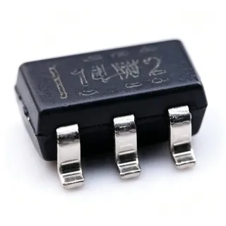
TLV3701IDBVR - Nanopower Push-Pull Comparator | Texas Instruments
Teilenummer: TLV3701IDBVR ✓ Aktiv| Menge | Stückpreis | Gesamt |
|---|---|---|
| 1 | $1.51 | $1,51 |
| 10 | $1.36 | $13,60 |
| 100 | $1.2 | $120,00 |
| 500 | $1.05 | $525,00 |
| 1.000 | $0.92 | $920,00 |
| 3.000 | $0.78 | $2.340,00 |
TLV3701IDBVR Übersicht
A comparator is an analog circuit that compares two input voltages and produces a digital output indicating which is larger; the push-pull CMOS output stage of the TLV3701 drives a rail-to-rail logic level without an external pull-up resistor. As a member of the comparator family within the broader signal-chain IC hierarchy, the TLV3701 belongs to the nanopower class, designed specifically for ultra-low quiescent current applications where battery life is paramount.
Key features include 560 nA quiescent current per channel, a typical propagation delay of 22 microseconds at 5 V, 18 V input tolerance with reverse-battery protection, and CMOS push-pull output capable of driving standard CMOS or TTL loads directly. The device also integrates ESD protection cells on the pins exceeding 2 kV HBM, and the SOT-23-5 package occupies only 2.9 mm x 1.6 mm of board area, enabling high-density PCB layouts.
Technically, the TLV3701 uses a CMOS architecture with an internal bandgap reference for the threshold, an input stage tolerant of rail-to-rail common-mode swings, and a symmetrical push-pull output driver. The slow 22 us propagation delay is the deliberate trade-off for achieving sub-microamp quiescent current; the part is not suited for high-speed signal conditioning but is engineered for monitoring tasks that change state infrequently.
Typical applications include battery voltage monitoring in wireless sensor nodes, low-frequency threshold detection in portable medical devices, micropower window comparators, system reset supervision, and battery-powered security sensors. The wide 2.7-16 V supply range also makes it suitable for industrial 24 V (nominal) line monitoring when divided down by external resistors.
When designing with this device, place a 0.1 uF bypass capacitor within 2 mm of the VCC pin and minimize input trace lengths to reduce parasitic coupling. The slow propagation means it should not be used in fast closed-loop control, but for monitoring battery voltage or generating wake-up signals in IoT devices, the 560 nA supply current is the headline advantage.
This page synthesizes distributor pricing, drop-in alternatives, and practical design notes not found on the manufacturer product page, giving engineers an actionable comparison set for nanopower comparator selection.
Drop-in-Alternativen für TLV3701IDBVR – gleiches Gehäuse, Pin-kompatibel. Bauteile mit anderem Gehäuse, die eine PCB-Überarbeitung erfordern, sind ausgeschlossen.
Schnellvergleichstool – Wählen Sie Alternativbauteile für den Direktvergleich:
TLV3701IDBVT
✅ Drop-In📋 Referenzalternative (nicht im Katalog)
TLV3701IDBVRG4
✅ Drop-In📋 Referenzalternative (nicht im Katalog)
TLV3701IDBVTG4
✅ Drop-In📋 Referenzalternative (nicht im Katalog)
TLV3701CDBVTG4
✅ Drop-In📋 Referenzalternative (nicht im Katalog)
TLV3701QDBVREP
✅ Drop-In📋 Referenzalternative (nicht im Katalog)
MCP6541T-E/OTY
✅ Drop-In📋 Referenzalternative (nicht im Katalog)
TLV3701IDBVR Grenzwerte & elektrische Eigenschaften
| Number of Channels | 1 |
| Ausgangstyp | CMOS, Push-Pull, Rail-to-Rail |
| Supply Current (per channel) | 560 nA (typical) |
| Supply Voltage Range | 2.7 V to 16 V |
| Input Common-Mode Range | Exceeds rails by 200 mV (-0.2 V to VCC+0.2 V) |
| Propagation Delay (5 V) | 22 us (typical) |
| Input Reverse-Battery Protection | 18 V |
| Betriebstemperaturbereich | -40 C to +125 C (Industrial) |
| Package Type | SOT-23-5 (DBV) |
| Montageart | Surface Mount |
| ESD Protection (HBM) | >2 kV |
| RoHS-Status | Compliant |
| MSL-Level | 1 |
| Lead-Free | Yes |
TLV3701IDBVR Pin-Konfiguration
| Pin 1 | OUT — Push-pull CMOS comparator output |
| Pin 2 | V- — Negative supply (ground) |
| Pin 3 | IN+ — Non-inverting input |
| Pin 4 | IN- — Inverting input |
| Pin 5 | V+ — Positive supply (2.7 V to 16 V) |
Typische Anwendungen
TLV3701IDBVR ist geeignet für 6 Anwendungs: Battery Voltage Monitoring, Wireless Sensor Node Threshold Detection, Portable Medical Monitoring, System Reset / Voltage Supervisor, Industrial 24V Line Monitor, Battery-Powered Security Sensor.
Battery Voltage Monitoring
The TLV3701IDBVR's 560 nA quiescent current makes it ideal for continuous battery voltage monitoring in wireless sensor nodes and IoT devices where battery life must exceed one year on a single cell. The 2.7 V to 16 V supply range accepts 1-cell Li-ion (3.7 V nominal), multi-cell alkaline stacks, and divided industrial rails. The push-pull CMOS output drives a microcontroller ADC trigger or interrupt pin directly without external pull-up resistors. Compared to a traditional LM393 solution, the TLV3701 reduces monitor current consumption by 350x, extending shelf life and field deployment intervals significantly. The 22 us propagation delay is more than adequate for periodic voltage sampling at sub-kHz rates.
Empfohlen
Wireless Sensor Node Threshold Detection
The TLV3701IDBVR serves as an ultra-low-power threshold detector in wireless sensor networks, where it continuously monitors a sensor signal against a reference voltage. Its 560 nA supply current means the comparator itself draws less power than the quiescent drain of typical wireless MCUs. The input common-mode range exceeds both rails by 200 mV, allowing direct connection to rail-referenced sensor bridges without level shifting. The push-pull output wakes the host microcontroller only when an event crosses the threshold, enabling duty-cycled sleep modes that multiply battery life. The SOT-23-5 footprint occupies less than 5 mm squared, enabling miniature sensor packages.
Empfohlen
Portable Medical Monitoring
The TLV3701IDBVR's nanopower 560 nA consumption and 16 V supply tolerance suit portable medical monitoring devices such as glucose meters, pulse oximeters, and continuous wearable health monitors. According to TI datasheet application notes, the comparator's slow 22 us propagation delay is acceptable for vital-sign event detection where human physiology changes occur over seconds, not microseconds. The 18 V reverse-battery protection prevents damage from incorrect battery insertion in field-deployed devices. The push-pull output interfaces directly to low-power MCU GPIO without additional components, reducing BOM cost and board area in cost-sensitive medical electronics.
Empfohlen
System Reset / Voltage Supervisor
The TLV3701IDBVR implements a micropower voltage supervisor that holds a microcontroller in reset until the supply rail exceeds a programmed threshold. Using an external resistor divider from VCC to the inverting input, the comparator switches state when VCC crosses the divider-set threshold, releasing reset via its push-pull output. At 560 nA, the supervisor adds negligible quiescent load to the battery, unlike dedicated supervisor ICs that often draw 1-10 uA. The 2.7 V to 16 V range covers 3.3 V logic systems through 12 V battery stacks. The SOT-23-5 package fits reset circuits that previously required SOIC-8 supervisor ICs.
Empfohlen
Industrial 24V Line Monitor
The TLV3701IDBVR monitors industrial 24 V (nominal) control lines when the input is divided down by external resistors to fit within the 16 V supply range. Its 560 nA draw is negligible compared to the milliamp-class currents typical in industrial PLC inputs. The reverse-battery 18 V input tolerance survives miswiring during field installation. The push-pull output drives opto-isolator LEDs directly without a series resistor in some configurations, simplifying the input stage. Operating temperature range of -40 C to +125 C supports outdoor and factory-floor deployment where ambient temperatures vary widely.
Empfohlen
Battery-Powered Security Sensor
The TLV3701IDBVR enables battery-powered security sensors (PIR motion detectors, glass-break detectors, door/window contacts) that must operate for years on a single battery. The 560 nA quiescent current means the comparator itself uses less power than typical coin-cell self-discharge rates. The input common-mode range accommodates battery voltage swings from fresh to end-of-life without requiring a separate reference. The push-pull CMOS output drives an RF transmitter enable pin or MCU interrupt directly. The SOT-23-5 package fits inside miniature sensor housings, and the wide supply range accepts 3 V lithium and 9 V battery stacks with the same circuit topology.
Empfohlen
Zusammenfassung der empfohlenen Produkte
Technische Referenzdaten für TLV3701IDBVR – Vergleich, Designhinweise und Compliance-Informationen.
Auswahlhilfe
Vergleich mit Alternativen
| Parameter | Dieses Produkt | TLV3701IDBVT | TLV3701IDBVRG4 | TLV3701QDBVREP | TLV3701CDBVTG4 | MCP6541T-E/OTY |
|---|---|---|---|---|---|---|
| Brand | Texas Instruments | Texas Instruments | Texas Instruments | Texas Instruments | Texas Instruments | Microchip Technology |
| Package | SOT-23-5 (DBV) | SOT-23-5 (DBV) - same | SOT-23-5 (DBV) - same | SOT-23-5 (DBV) - same | SOT-23-5 (DBV) - same | SOT-23-5 - same |
| Quiescent Current | 560 nA | 560 nA | 560 nA | 560 nA | 560 nA | ~1 uA |
| Supply Voltage Range | 2.7 V to 16 V | 2.7 V to 16 V | 2.7 V to 16 V | 2.7 V to 16 V | 2.7 V to 16 V | 1.6 V to 5.5 V |
| Output Type | CMOS Push-Pull | CMOS Push-Pull | CMOS Push-Pull | CMOS Push-Pull | CMOS Push-Pull | CMOS Push-Pull |
| Operating Temperature | -40 C to +125 C | -40 C to +125 C | -40 C to +125 C | -40 C to +125 C (AEC-Q100) | 0 C to +70 C | -40 C to +125 C |
| Automotive Qualified | No | No | No | Yes (AEC-Q100) | No | No |
Wichtigste Unterscheidungsmerkmale
- Nanopower 560 nA quiescent current (vs. LM393)
- Automotive-grade option in same footprint (vs. TLV3701IDBVR (standard))
- Wide supply voltage range (vs. MCP6541T-E/OTY)
Designhinweise
The TLV3701IDBVR's 560 nA quiescent current makes it suitable for always-on battery monitoring, but ensure that all other circuit blocks (resistor dividers, reference circuits) consume a similar order of magnitude. Estimated: a 1 MOhm input divider draws 3.3 V / 1 MOhm = 3.3 uA - 6x more than the comparator itself. Use high-impedance dividers (10 MOhm+) or pulsed measurement topologies to keep total quiescent below 1 uA in battery-powered designs.
Place a 0.1 uF ceramic bypass capacitor within 2 mm of the VCC pin (pin 5) to suppress supply noise. For battery-powered applications with long wire harnesses, add a 10 uF bulk capacitor near the comparator to handle transient currents when the output switches. Route input traces away from switching nodes to prevent false triggering; the comparator's 22 us propagation delay provides some noise immunity but cannot reject fast transients coupling through high-impedance inputs.
Do not use the TLV3701IDBVR for high-speed signal conditioning - its 22 us propagation delay is too slow for audio, video, or data comparator applications. Choose TLV3201 instead when response time is critical. Also note that the slow propagation delay means the input must remain stable for at least 30-50 us to ensure reliable output transition - do not use with high-frequency oscillating signals without hysteresis.
Compliance-Informationen
Standard TLV3701IDBVR is not AEC-Q100 qualified; choose TLV3701QDBVREP variant for automotive. RoHS compliant per TI product page.