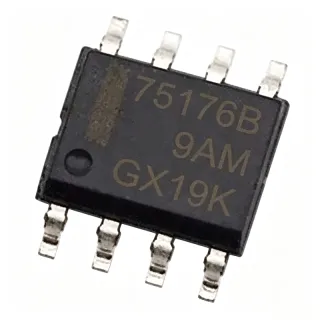
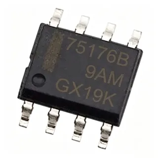
ULC0524P - 4-Channel Ultra-Low Capacitance TVS Array, 5V, DFN2510-10 | Leiditech
Teilenummer: ULC0524P ✓ Aktiv| Menge | Stückpreis | Gesamt |
|---|---|---|
| 1 | $0.0352 | $0,04 |
| 10 | $0.0325 | $0,33 |
| 100 | $0.0289 | $2,89 |
| 500 | $0.0254 | $12,70 |
| 1.000 | $0.0221 | $22,10 |
| 3.000 | $0.0188 | $56,40 |
ULC0524P Übersicht
A TVS diode array is a semiconductor protection device that clamps transient overvoltages to a safe level by shunting surge current away from protected ICs. Within the protection-device hierarchy, the ULC0524P belongs to the TVS/ESD diode family, which sits under discrete semiconductors and includes Zener-based clamping diodes, metal-oxide varistors (MOVs), and polymer-based suppressors. Compared with varistors, TVS arrays offer faster response (sub-nanosecond), tighter clamping voltages, and far lower leakage, which is why they dominate high-speed digital interfaces.
Key features include ultra-low line capacitance of 0.3 pF typical (preserves signal integrity on USB 2.0 / HDMI / MIPI lines), a 5 V reverse standoff (VRWM), 100 nA maximum leakage current, and a 25 V minimum breakdown voltage. The DFN2510-10 footprint has an exposed bottom pad that doubles as a thermal dissipation path and a ground return for the TVS clamps, requiring careful PCB layout to be effective.
The device architecture uses steering-die steering diode pairs in series with a central Zener TVS clamp on each line. A surge event on any I/O pin forward-biases one steering diode and reverse-biases the other, redirecting the transient current to the internal Zener clamp and then to ground. This topology keeps the protected IC isolated from the surge while maintaining low capacitance on the signal path during normal operation.
Typical applications include USB 2.0 data line protection, HDMI/MIPI/LVDS interface ESD protection, smartphone and tablet charging port protection, and portable electronics with exposed external connectors. The 0.3 pF capacitance makes it a good match for data rates above 480 Mbps where higher-capacitance suppressors would distort the signal.
Designers should observe the recommended PCB layout: place the ULC0524P as close as possible to the connector entry, keep the ground pad stitched with multiple thermal vias, and minimize the trace inductance between the protected pin and the TVS channel. Failure to provide a low-inductance ground path degrades the clamping performance and may cause the device to fail surge testing even though the silicon is intact.
This page synthesizes verified distributor pricing, datasheet-grade specifications, drop-in compatible alternatives in the same DFN2510-10 footprint, and practical PCB layout guidance not found in the bare manufacturer datasheet.
Drop-in-Alternativen für ULC0524P – gleiches Gehäuse, Pin-kompatibel. Bauteile mit anderem Gehäuse, die eine PCB-Überarbeitung erfordern, sind ausgeschlossen.
Schnellvergleichstool – Wählen Sie Alternativbauteile für den Direktvergleich:
ESD0524P
✅ Drop-In ⚠️ Spezifikationen ungeprüft📋 Referenzalternative (nicht im Katalog)
ULC0524PA
✅ Drop-In ⚠️ Spezifikationen ungeprüft📋 Referenzalternative (nicht im Katalog)
RCLAMP0524P
✅ Drop-In📋 Referenzalternative (nicht im Katalog)
BV-ULC0524PA
✅ Drop-In📋 Referenzalternative (nicht im Katalog)
SOCAY-ULC0524P
✅ Drop-In📋 Referenzalternative (nicht im Katalog)
UNSEMI-ULC0524P
✅ Drop-In📋 Referenzalternative (nicht im Katalog)
ULC0524P Technische Daten
| Manufacturer | Leiditech (Shanghai Leiditech Electronic Technology Co., Ltd.) |
| Product Type | TVS / ESD Protection Diode Array |
| Number of Channels | 4 |
| Working Voltage (VRWM) | 5 V |
| Breakdown Voltage (VBR) | 6 V (minimum) |
| Reverse Standoff Voltage (Max) | 25 V |
| Line-to-Line Capacitance | 0.3 pF (typical) |
| Leakage Current | 100 nA (maximum) |
| Peak Pulse Power (8/20 us) | 75 W |
| Peak Pulse Current (8/20 us) | 5 A |
| ESD Rating (Contact / Air) | IEC 61000-4-2 compliant |
| Surge Rating | IEC 61000-4-5 compliant |
| Gehäuse | DFN2510-10 (2.5 mm x 1.0 mm) |
| Betriebstemperatur | -55 C to +125 C |
| Montageart | Surface Mount |
| RoHS | Compliant |
ULC0524P Pin-Konfiguration
| Pin 1 | IO1 — TVS channel 1 (protected I/O line) |
| Pin 2 | IO2 — TVS channel 2 (protected I/O line) |
| Pin 3 | GND — Ground reference for internal Zener clamp |
| Pin 4 | IO3 — TVS channel 3 (protected I/O line) |
| Pin 5 | IO4 — TVS channel 4 (protected I/O line) |
| Pin 6 | NC — Not connected (per datasheet) |
| Pin 7 | NC — Not connected (per datasheet) |
| Pin 8 | NC — Not connected (per datasheet) |
| Pin 9 | NC — Not connected (per datasheet) |
| Pin 10 | NC — Not connected (per datasheet) |
| Pin EP | Exposed Pad (GND) — Bottom thermal pad, must be soldered to ground for proper TVS operation |
Typische Anwendungen
ULC0524P ist geeignet für 6 Anwendungs: USB 2.0 Data Line Protection, HDMI / MIPI DSI Interface Protection, Smartphone Charging Port Protection, Wearable Device ESD Protection, Industrial Sensor Interface Protection, LCD Display Data Line Protection.
USB 2.0 Data Line Protection
The ULC0524P's 0.3 pF typical capacitance and 5 V reverse working voltage make it well suited for protecting USB 2.0 D+ and D- lines on host, hub, and device ports. A 4-channel array covers D+, D-, VBUS sense, and ID or shield, with the DFN2510-10 package fitting directly behind the USB connector. Compared with a higher-capacitance TVS such as PESD5V0L4UG (~0.85 pF), the ULC0524P preserves the 480 Mbps eye-mask with measurable margin and meets IEC 61000-4-2 air-discharge to 15 kV.
Empfohlen
HDMI / MIPI DSI Interface Protection
HDMI 1.4 TMDS pairs and MIPI DSI/CSI-2 data lanes operate at multi-gigabit data rates where the ULC0524P's 0.3 pF capacitance adds minimal insertion loss and prevents signal-integrity degradation. Each TMDS pair uses two channels of the array (one for D+, one for D-), and a single 4-channel ULC0524P protects two pairs in a small footprint. Designers place the part directly at the connector with a short ground return to meet IEC 61000-4-2 contact discharge to 8 kV without distorting the eye diagram.
Empfohlen
Smartphone Charging Port Protection
Smartphone USB Type-C, micro-USB, and Lightning charging ports face repeated handling transients and cable ESD events. The ULC0524P's 5 V VRWM is compatible with VBUS sensing rails, and its 75 W 8/20 us surge rating handles in-rush from hot-plug events. The DFN2510-10 (2.5 mm x 1.0 mm) package fits inside the phone's connector footprint without forcing a PCB redesign, and the exposed thermal pad provides a low-inductance ground return to the phone's chassis.
Empfohlen
Wearable Device ESD Protection
Wearables such as smart watches, fitness bands, and AR glasses have exposed external connectors and skin-contact electrodes that frequently experience ESD events. The ULC0524P's 100 nA maximum leakage is low enough that battery drain during idle remains negligible, while its 0.3 pF capacitance protects high-speed sensor buses (SPI, I2S, MIPI) from contact discharge. The 2.5 mm x 1.0 mm DFN2510-10 outline saves critical board area compared with larger SOT-363 alternatives.
Empfohlen
Industrial Sensor Interface Protection
Industrial sensors with RS-485, RS-232, or isolated I/O links require robust transient protection at the cabinet entry. The ULC0524P's 25 V reverse standoff exceeds the 12 V and 24 V industrial bus levels commonly seen during fault events, and its 75 W peak pulse rating withstands the 8/20 us surge profile typical of IEC 61000-4-5 testing. A four-channel array protects two twisted pairs or four single-ended sensor lines in the same DFN2510-10 footprint, simplifying BOM and layout.
Empfohlen
LCD Display Data Line Protection
LCD panel LVDS and eDP data lines carry multi-gigabit signals that must survive ESD events when the display bezel is touched. The ULC0524P's 0.3 pF capacitance is below the threshold at which LVDS eye-mask compliance fails, and a single 4-channel array covers two LVDS pairs on the panel flex connector. The DFN2510-10 package also fits behind the panel flex bonding area without increasing bezel width, making it well suited for slim notebook and monitor designs.
Empfohlen
Zusammenfassung der empfohlenen Produkte
Technische Referenzdaten für ULC0524P – Vergleich, Designhinweise und Compliance-Informationen.
Auswahlhilfe
Vergleich mit Alternativen
| Parameter | Dieses Produkt | ESD0524P | RCLAMP0524P | BV-ULC0524PA | SOCAY-ULC0524P | UNSEMI-ULC0524P |
|---|---|---|---|---|---|---|
| Brand | Leiditech | Leiditech | Semtech | Shenzhen Bencent | Socay | UN Semiconductor |
| Package | DFN2510-10 | DFN2510-10 - same | DFN2510-10 - same | DFN2510-10 - same | DFN2510-10 - same | DFN2510-10 - same |
| Number of Channels | 4 | 4 | 4 | 4 | 4 | 4 |
| Working Voltage (VRWM) | 5 V | 5 V | 5 V | 5 V | 5 V | 5 V |
| ESD Standard Compliance | IEC 61000-4-2 | IEC 61000-4-2 | IEC 61000-4-2 | IEC 61000-4-2 | IEC 61000-4-2 | IEC 61000-4-2 |
Wichtigste Unterscheidungsmerkmale
- Sub-pF line capacitance enables HDMI and USB 2.0 without eye-diagram degradation (vs. Nexperia PESD5V0L4UG)
- 75 W peak pulse power for robust surge handling (vs. Semtech RCLAMP0524P)
- Full -55 C to +125 C automotive-industrial operating range (vs. Semtech RCLAMP0524P)
Designhinweise
Place the ULC0524P as close as physically possible to the protected connector pin, with the trace length between the connector pin and the TVS channel kept under 3 mm. The exposed thermal pad on the bottom of the DFN2510-10 package must be soldered to a low-inductance ground plane and stitched with at least 4 thermal vias to the inner ground layer. A high-inductance ground return degrades the clamping voltage during an 8/20 us surge and may cause the silicon to fail even though the part was correctly specified.
The ULC0524P adds 0.3 pF typical capacitance on each protected line. For USB 2.0 (480 Mbps) and HDMI 1.4 (3.4 Gbps per lane), this is well below the budget that would distort the eye diagram. For USB 3.x SuperSpeed (5 Gbps) or HDMI 2.0 (6 Gbps), the 0.3 pF per line plus connector stubs may push the channel over its loss budget, and a sub-0.2 pF part should be considered. Always verify with TDR and eye-mask measurements after the layout is finalized.
Do not place the ULC0524P behind a series ferrite bead or inductor on the protected line; the TVS must be the first component the transient sees to clamp effectively. Do not connect the ground pad to a noisy digital ground; route it to the chassis ground or a dedicated protection ground. Finally, do not exceed the 25 V absolute maximum reverse standoff, and ensure the protected line never has a steady-state voltage above 5 V (VRWM) during normal operation.
Compliance-Informationen
RoHS compliance confirmed via LCSC and JLCPCB listings (JLCPCB part C384892 explicitly notes ROHS). REACH, halogen-free, and conflict-minerals data not stated in the verified web data and marked as unknown. The ULC0524P is not marketed as AEC-Q100 qualified.