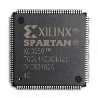
XC6SLX4-L1TQG144C - 3840-Cell Spartan-6 LX FPGA | AMD
Teilenummer: XC6SLX4-L1TQG144C ✓ AktivXC6SLX4-L1TQG144C Übersicht
A field-programmable gate array is a semiconductor whose digital logic is configured after manufacture. The FPGA category combines programmable logic blocks, memory, input/output resources, clocking, and configuration circuitry into one reconfigurable device. Within the AMD Spartan-6 LX family, the XC6SLX4 provides a comparatively compact implementation for designs that need moderate logic density without moving to a larger device or package.
The device offers 3,840 logic cells, 102 user I/O, a 45 nm CMOS process, and a 1 V core voltage. Its 144-LQFP package exposes the full Spartan-6 LX4 I/O and configuration interface while remaining compatible with conventional board-assembly and inspection processes. The L1 designation identifies a specific speed-grade ordering option, while the terminal suffix identifies the TQG144 package and C temperature-market option.
Spartan-6 LX devices support parallel and serial configuration paths, including boundary-scan JTAG programming described for this device. Boundary scan permits configuration data to be loaded through dedicated JTAG pins, supporting board-level programming and manufacturing test. Designers can also reuse the same pin-compatible family across designs when logic capacity, speed grade, or temperature-market suffix permits, provided the selected ordering option matches the design requirements.
Typical implementations include industrial control panels, programmable logic controllers, sensor aggregation systems, communications interface modules, test equipment, and low-to-moderate complexity embedded-processing platforms. The combination of 102 I/O and 3,840 logic cells is useful when a design needs many external connections without the resource level of a larger Spartan-6 device. The 144-LQFP package also simplifies prototype assembly compared with fine-pitch ball-grid-array packages.
Designs must account for configuration startup, clocking, decoupling, and signal-integrity requirements before schematic capture. Bank supply planning, VCCO requirements, JTAG access, and unused pins should be checked against the Spartan-6 pinout and configuration guidance. A one-volt core rail should be generated with appropriate sequencing and noise control, while I/O supply selection must remain compatible with the voltage standards used by connected devices.
This product page combines package, logic-resource, interface, and ordering information with practical design guidance, compatible same-brand ordering options, and a parameter-by-parameter comparison. These details help engineers distinguish speed-grade and temperature-market changes before modifying an existing 144-LQFP Spartan-6 LX4 design.
Drop-in-Alternativen für XC6SLX4-L1TQG144C – gleiches Gehäuse, Pin-kompatibel. Bauteile mit anderem Gehäuse, die eine PCB-Überarbeitung erfordern, sind ausgeschlossen.
Varianten dieser Serie
Modelle derselben Serie, die drop-in-kompatibel sind mit XC6SLX4-L1TQG144C (gleiche Bauform und Footprint) – abweichend in Package, Block RAM, Process Technology, Logic Cells, Speed Grade.
XC6SLX4-2TQG144C
✅ Drop-InPreis auf Anfrage
Datenblatt ansehen →XC6SLX4-2TQG144I
✅ Drop-InPreis auf Anfrage
Datenblatt ansehen →XC6SLX4-3TQG144C
✅ Drop-InPreis auf Anfrage
Datenblatt ansehen →XC6SLX4-L1TQG144C Grenzwerte & elektrische Eigenschaften
| Device Type | Spartan-6 LX field-programmable gate array |
| Logic Cells | 3,840 cells |
| User I/O | 102 I/O |
| Process Technology | 45 nm CMOS |
| Core Supply Voltage | 1 V |
| Gehäuse | 144-LQFP |
| Terminal Count | 144 terminals |
| Package Type | Quad Flat Package |
| Montagestil | Surface mount |
| Configuration Interface | JTAG boundary scan |
| Programmable Logic Type | Spartan-6 LX FPGA |
| Ordering Speed Designator | L1 |
| Package Code | TQG144 |
| Temperature-Market Suffix | C |
XC6SLX4-L1TQG144C tqg144 Pinbelegungsleitfaden
Pinbelegung für XC6SLX4-L1TQG144C (tqg144-Gehäuse). Dieser digitale IC umfasst GPIO, Kommunikationsschnittstellen (UART, SPI, I2C) und Versorgungspins. Alternative Pin-Funktionen und Konfigurationsoptionen entnehmen Sie dem Herstellerdatenblatt. Unverzichtbar für Embedded-System-Design und PCB-Layout.

Keine detaillierten Pinbelegungsdaten verfügbar für XC6SLX4-L1TQG144C.
Siehe die Datenblatt für die vollständige Pin-Konfiguration.
Typische Anwendungen
XC6SLX4-L1TQG144C ist geeignet für 6 Anwendungs: Industrial Control and Automation, Communications Interface Module, Sensor Aggregation and Signal Conditioning, Programmable Logic Controller, Test and Measurement Equipment, Embedded Processing Platform.
Industrial Control and Automation
The XC6SLX4-L1TQG144C fits compact industrial controllers that coordinate sensors, actuators, interlocks, and machine-status logic. Its 3,840 logic cells can host parallel control functions, while 102 user I/O provides substantial connectivity in a 144-LQFP package. The 1 V core and separate I/O supplies should be planned with appropriate sequencing and decoupling. Designers must also verify the C temperature-market option against the enclosure temperature, vibration, noise, and isolation requirements of the target industrial equipment.
Empfohlen
Communications Interface Module
The Spartan-6 LX4 FPGA can implement protocol conversion, framing, buffering, and supervisory logic for communications equipment. Its 102 user I/O allows multiple parallel interfaces to coexist, while the 3,840-cell capacity is appropriate for moderate-throughput data paths rather than demanding processor cores. The 144-LQFP footprint simplifies routing into conventional equipment chassis. Interface timing, clock domains, impedance, and I/O voltage standards must be established before configuration, and a faster grade should be selected only after checking setup and hold margins.
Empfohlen
Sensor Aggregation and Signal Conditioning
XC6SLX4-L1TQG144C is suitable for acquiring and conditioning inputs from multiple sensors, performing digital filtering, thresholding, diagnostics, and data packing. With 102 user I/O, the device can connect parallel sensor channels and associated control signals without requiring the pin density of a larger FPGA package. Its 3,840 logic cells support modest parallel logic and control blocks. Designers should reserve clock-capable pins, define input thresholds through the complete signal chain, and verify that the selected package and temperature-market suffix match the measurement environment.
Empfohlen
Programmable Logic Controller
The XC6SLX4-L1TQG144C can serve as the programmable core of a small PLC or embedded sequencer because its 3,840 logic cells and 102 I/O accommodate parallel state machines, timers, interlocks, and communication interfaces. The 144-LQFP package provides a practical route for serviceable and visually inspectable control boards. Because deterministic behavior depends on configuration integrity and clocking, designers should validate startup behavior, watchdog handling, I/O isolation, and supply sequencing. A faster replacement can alter timing and dynamic power rather than simply increasing application capacity.
Empfohlen
Test and Measurement Equipment
The Spartan-6 LX4 device is applicable to programmable test systems, waveform generation, fixture control, timing controllers, and measurement-interface logic. Its 102 I/O supports multiple instrument and DUT connections, while the programmable architecture enables reusable sequencing and analysis functions. The 1 V core rail requires careful decoupling and clock distribution to preserve measurement quality. Engineers should assign clock-capable pins deliberately, control output transitions where needed, and confirm the 144-LQFP package keeps adequate creepage and clearance for the intended voltage levels.
Empfohlen
Embedded Processing Platform
The XC6SLX4-L1TQG144C can support modest embedded workloads involving parallel logic, bus arbitration, state-machine control, and dedicated hardware acceleration alongside a separate processor. Its 3,840 logic cells are useful for peripheral interfaces and fixed-function datapaths, while 102 I/O leave sufficient external connectivity for memory and communications. The 144-LQFP package makes prototype assembly and rework straightforward. System partitioning must preserve the FPGA’s fixed I/O, clock, configuration, and supply requirements, and timing should be rechecked for every speed-grade substitution.
Empfohlen
Zusammenfassung der empfohlenen Produkte
Technische Referenzdaten für XC6SLX4-L1TQG144C – Vergleich, Designhinweise und Compliance-Informationen.
Auswahlhilfe
Vergleich mit Alternativen
| Parameter | Dieses Produkt | XC6SLX4-2TQG144C | XC6SLX4-2TQG144I | XC6SLX4-3TQG144C |
|---|---|---|---|---|
| Package | 144-LQFP (TQG144) | 144-LQFP (TQG144) | 144-LQFP (TQG144) | 144-LQFP (TQG144) |
| Brand | AMD | AMD | AMD | AMD |
| FPGA Family | Spartan-6 LX | Spartan-6 LX | Spartan-6 LX | Spartan-6 LX |
| Logic Cells | 3,840 cells | 3,840 cells | 3,840 cells | 3,840 cells |
| User I/O | 102 I/O | 102 I/O | 102 I/O | 102 I/O |
| Process Technology | 45 nm CMOS | 45 nm CMOS | 45 nm CMOS | 45 nm CMOS |
| Core Supply Voltage | 1 V | 1 V | 1 V | 1 V |
| Speed Designator | L1 | Grade 2 | Grade 2 | Grade 3 |
| Temperature-Market Suffix | C | C | I | C |
Wichtigste Unterscheidungsmerkmale
- Matches the 3,840-cell Spartan-6 LX4 architecture while preserving a 144-LQFP footprint (vs. XC6SLX4-2TQG144C)
- Maintains footprint compatibility with a higher speed-grade option (vs. XC6SLX4-3TQG144C)
- Offers a same-footprint migration toward an industrial-temperature ordering option (vs. XC6SLX4-2TQG144I)
Designhinweise
Use the manufacturer’s Spartan-6 power-tree and decoupling recommendations for the 1 V core rail and applicable I/O supplies. Keep the core and I/O supply paths separate through the PCB power network, place high-frequency decoupling close to the device, and account for startup current when selecting regulators and bulk capacitance. Supply sequencing must remain compatible with configuration behavior. Estimated conversion loss cannot be stated without the design’s input voltage, output current, efficiency, and thermal data.
Assign configuration pins, clock-capable pins, VCCO banks, and user I/O directly from the official 144-TQG package files before signal routing. Keep JTAG access unobstructed for production programming and boundary-scan test. For interfaces using fast edges, control trace lengths, provide continuous reference planes, avoid unnecessary stubs, and terminate according to the actual signal standard. Do not infer analog performance or signal integrity from the nominal FPGA logic-cell count.
A same-package replacement does not automatically satisfy every requirement. Compare the exact speed designator, temperature-market suffix, configuration method, supported I/O standards, clock behavior, and power characteristics before changing the bill of materials. In particular, grade 2 and grade 3 options may alter timing margins and dynamic power. Revalidate the complete design after substituting a faster grade rather than assuming that all configuration files and constraints remain interchangeable.
The 144-LQFP package exposes its leads on all four sides and requires adequate copper area and thermal via placement beneath or near the device when utilization is high. Follow the manufacturer’s package thermal guidance for the board stack-up and airflow condition. Estimated junction temperature requires the selected package thermal resistance, actual dissipation, and ambient temperature, so those values must be taken from the design data before assigning a thermal margin.
Compliance-Informationen
The target is an FPGA rather than an automotive-qualified discrete or power component. Specific RoHS, REACH, lead-free, halogen-free, and conflict-minerals declarations should be confirmed from the current AMD product documentation or declaration for the exact ordering code.