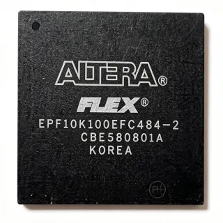
XC7A75T-2FG484I - 75,520-LCELL Artix-7 FPGA | AMD | 484-BBGA
Teilenummer: XC7A75T-2FG484I ✓ Aktiv| Menge | Stückpreis | Gesamt |
|---|---|---|
| 1 | $41.1231 | $41,12 |
| 10 | $41.1231 | $411,23 |
| 100 | $41.1231 | $4.112,31 |
| 500 | $41.1231 | $20.561,55 |
| 1.000 | $41.1231 | $41.123,10 |
XC7A75T-2FG484I Übersicht
An FPGA is a programmable digital integrated circuit that combines configurable logic, memory, digital signal processing, and parallel I/O within one semiconductor. Artix-7 belongs to AMD's 7-series FPGA family and targets compact systems requiring substantial parallel processing, flexible interfaces, hardware acceleration, or programmable control without the resource level of a larger FPGA. Its logic density makes it useful between small microcontroller-class devices and high-end programmable logic systems.
The verified specifications identify 75,520 logic cells and 285 I/O in a 484-BBGA package. The related package-file result confirms that Artix-7 package pinout files are available in ASCII TXT and CSV formats, enabling board-level design and signal verification. The package data also associates this device with a 1.0 V supply and an extended -40°C to +100°C temperature range, making it suitable for industrial and embedded environments when the complete electrical and timing requirements are satisfied.
Typical uses include industrial automation, embedded control, parallel data acquisition, communications, test equipment, and hardware-assisted signal processing. The FPGA can implement multiple digital functions in parallel, such as interfaces, state machines, protocol handling, counters, and custom processing pipelines. The 484-BBGA package requires careful ball-escape routing, multilayer PCB construction, controlled power delivery, and thermal analysis; it is not a simple through-hole or two-pin package.
Designers should use AMD's package pinout files and Artix-7 datasheet to verify every ball assignment, power rail, decoupling requirement, and configuration connection. A power rail must meet the specified voltage and sequencing requirements, and unused balls must be handled exactly as directed by the manufacturer. Confirm the complete device configuration, supported I/O standards, speed grade, and industrial-temperature requirements before release.
This product page consolidates verified distributor pricing and availability, package information, practical FPGA design notes, and qualified comparison fields. Values not present in the supplied source data remain explicitly marked for validation rather than being guessed.
Drop-in-Alternativen für XC7A75T-2FG484I – gleiches Gehäuse, Pin-kompatibel. Bauteile mit anderem Gehäuse, die eine PCB-Überarbeitung erfordern, sind ausgeschlossen.
Schnellvergleichstool – Wählen Sie Alternativbauteile für den Direktvergleich:
Für dieses Produkt sind keine Drop-in-Alternativen verfügbar.
Alternativen anfordernXC7A75T-2FG484I Grenzwerte & elektrische Eigenschaften
| Device Type | Artix-7 Field Programmable Gate Array (FPGA) |
| Programmable Logic Cells | 75,520 cells |
| I/O Count | 285 I/Os |
| Adaptive Logic Modules | 11,800 ALMs |
| Embedded Memory | 3.69 Mbit |
| Versorgungsspannung | 1.0 V |
| Betriebstemperatur | -40°C to +100°C |
| Gehäuse | 484-BBGA |
| Package Family | FBGA |
| Montageart | Surface Mount |
| FPGA Family | Artix-7 |
| Technology | 28 nm |
| Product Category | Field Programmable Gate Array (FPGA) |
| Logic Resource Count | 75520 |
XC7A75T-2FG484I fbga Pinbelegungsleitfaden
Pinbelegung für XC7A75T-2FG484I (fbga-Gehäuse). Dieser digitale IC umfasst GPIO, Kommunikationsschnittstellen (UART, SPI, I2C) und Versorgungspins. Alternative Pin-Funktionen und Konfigurationsoptionen entnehmen Sie dem Herstellerdatenblatt. Unverzichtbar für Embedded-System-Design und PCB-Layout.

Keine detaillierten Pinbelegungsdaten verfügbar für XC7A75T-2FG484I.
Siehe die Datenblatt für die vollständige Pin-Konfiguration.
Typische Anwendungen
XC7A75T-2FG484I ist geeignet für 6 Anwendungs: Industrial Automation Controller, Data Acquisition System, Communications Interface, Test and Measurement Equipment, Embedded Signal Processing, Embedded Networking and Storage.
Industrial Automation Controller
The AMD XC7A75T-2FG484I fits industrial automation when a controller needs parallel logic, multiple interfaces, and programmable hardware behavior. Its verified 75,520 logic cells, 11,800 ALMs, 3.69 Mbit of embedded memory, and 285 I/Os can support motion sequencing, sensor conditioning logic, communications, and machine-control functions in parallel. The -40°C to +100°C listed range is relevant to equipment exposed to industrial temperature conditions. Designers should use the matching 484-BBGA package files, validate power sequencing and decoupling, and confirm every supported I/O standard before releasing the PCB. The FPGA is useful when deterministic parallel processing or flexible logic capacity matters more than using a smaller fixed microcontroller.
Empfohlen
Data Acquisition System
XC7A75T-2FG484I is well suited to data-acquisition front ends that require parallel sampling, digital filtering, buffering, and interface control implemented in programmable logic. The verified 285 I/Os provide a substantial parallel interface surface, while 3.69 Mbit of embedded memory can support local data storage and processing. A practical architecture can place ADC control, capture logic, digital filtering, and a communication interface in one programmable device. Designers must verify acquisition-clock timing, input-voltage tolerances, I/O standards, and power sequencing against the complete AMD documentation. The 484-BBGA package also demands careful layer transitions and return-path planning to preserve data integrity across the FPGA.
Empfohlen
Communications Interface
The XC7A75T-2FG484I can implement communications protocols, packet handling, framing, and interface bridges in parallel hardware. Its 75,520 logic cells provide capacity for multiple parallel lanes and protocol state machines, and the 285 I/Os support device interfacing when the selected electrical standards are confirmed. A useful design may combine a physical interface, transmit and receive buffers, CRC logic, and a host or memory interface. The 1.0 V listed supply is a design input, but all rails, I/O voltage requirements, and configuration pins must be checked in the datasheet. Use controlled impedance routing and package-aware escape geometry for high-speed links rather than treating the FPGA as a generic logic IC.
Empfohlen
Test and Measurement Equipment
XC7A75T-2FG484I is appropriate for programmable test systems that combine timing control, pattern generation, acquisition, and data reduction in one FPGA. Its 75,520 logic cells and 11,800 ALMs can support parallel channels and independent control loops, while 3.69 Mbit of embedded memory can buffer local samples. The -40°C to +100°C listed operating range is useful for industrial test environments, subject to complete system qualification. Designers should define clocking, pin assignments, and I/O standards early, then use the AMD package files to validate every 484-BBGA ball. Power distribution, ground continuity, thermal management, and signal-integrity analysis are especially important when the FPGA drives precision or high-speed test circuitry.
Empfohlen
Embedded Signal Processing
The XC7A75T-2FG484I supports embedded signal-processing designs that benefit from parallel pipelines, configurable filters, and hardware acceleration. The verified FPGA resources include 75,520 logic cells, 11,800 ALMs, and 3.69 Mbit of embedded memory, enabling multiple processing stages to operate concurrently. Examples include digital filtering, FFT-like pipeline functions, modulation control, and sensor-signal conditioning. The 1.0 V device supply is identified in the verified data, but the complete power tree and configuration method must be confirmed before implementation. Place clock and high-speed data routes with short return paths, separate noisy switching or clock-adjacent circuits where appropriate, and verify timing closure using the selected speed-grade documentation.
Empfohlen
Embedded Networking and Storage
XC7A75T-2FG484I can act as a programmable interface controller between network or storage peripherals and a host processor. Its large verified logic-resource count supports protocol engines, packet buffers, and custom data-transfer paths, while 285 I/Os allow flexible connection to external controllers and memories. A design may implement a bridge, frame processor, or data-format converter instead of relying only on fixed hardware. The 484-BBGA package requires multilayer PCB routing and exact package-file verification; power and ground planes must support the listed 1.0 V device supply without excessive noise. Before layout, confirm supported memory interfaces, voltage standards, pin assignments, and whether the intended temperature range matches the assembly requirement.
Empfohlen
Zusammenfassung der empfohlenen Produkte
Technische Referenzdaten für XC7A75T-2FG484I – Vergleich, Designhinweise und Compliance-Informationen.
Auswahlhilfe
Vergleich mit Alternativen
| Parameter | Dieses Produkt |
|---|---|
| Brand | AMD |
| Device Type | Artix-7 FPGA |
| Package | 484-BBGA |
| Logic Cells | 75,520 |
| I/O Count | 285 I/Os |
| Adaptive Logic Modules | 11,800 ALMs |
| Embedded Memory | 3.69 Mbit |
| Supply Voltage | 1.0 V |
| Operating Temperature | -40°C to +100°C |
| Technology | 28 nm |
| Mounting Type | Surface Mount |
| Verified Starting Price | $41.1231 |
Wichtigste Unterscheidungsmerkmale
- Verified FPGA resource density (vs. XC7A75T-2FGG484I)
- Industrial temperature listing (vs. XC7A75T-2FGG484I)
- Documented package identity (vs. XC7A75T-2FTG256I)
Designhinweise
Treat the listed 1.0 V supply as the core device supply, but do not infer the complete power tree from that value. Verify all required rails, sequencing, decoupling, and power-current limits in the Artix-7 datasheet. Place the required bulk and high-frequency decoupling close to the 484-BBGA power balls, provide continuous plane connections, and keep return paths through the ball array rather than through narrow traces.
Use the matching AMD Artix-7 package pinout file for every 484-BBGA ball assignment. Plan escape routing according to the package geometry, preserve ball access, and maintain continuous reference planes beneath high-density signal escapes. Unused balls must be handled according to the manufacturer guidance rather than assigned experimentally.
A 484-BBGA FPGA needs a deliberate thermal path because heat must leave the device through its package and PCB structure. Check the package thermal data, estimate junction temperature using the actual board construction and airflow, and use copper planes, thermal vias, or other approved structures when required. Do not assume that a large exposed copper area alone guarantees the target junction temperature.
Compliance-Informationen
The supplied verified data does not state RoHS, REACH, AEC-Q100, lead-free, halogen-free, or conflict-minerals status. The Artix-7 device is an FPGA, so automotive qualification status is not established by the supplied information.