Productos (35.000+)

TLV571CDW - 8-Bit 1.25 MSPS ADC | Texas Instruments
TLV571CDW

TLV571CDW - 8-Bit 1.25 MSPS ADC | Texas Instruments

The Texas Instruments TLV571CDW is an 8-bit, single-channel, parallel-output analog-to-digital converter rated for 1.25 MSPS in the device family and 625 KSPS at a 3 V supply according to the manufacturer datasheet search result. It operates from 2.7 V to 5.5 V and accepts an analog input range from 0 V to AVDD. The device is packaged in a 16-pin SOIC package. An ADC is a data-acquisition IC that samples an analog voltage and converts it into a digital value. The TLV571 belongs to the ADC/DAC hierarchy and uses a successive-approximation, or SAR, conversion architecture. Its parallel interface provides eight digital output bits plus control and status signals, making it suitable for systems where a microcontroller, DSP, or other digital controller reads conversions without relying on a serial protocol. The verified manufacturer data identifies several useful features: 2.7 V to 5.5 V single-supply operation, 0 V to AVDD analog input range, differential and integral nonlinearity below ±0.5 LSB, and hardware configuration for DSP and microcontroller compatibility. The output can be binary or twos complement. Low-power operation is also emphasized, with 12 mW specified at 3 V and 35 mW at 5 V. Power management is handled through automatic power-down or software power-down, according to the manufacturer product description. Automatic power-down is listed at 1 mA maximum, while software power-down is listed at 10 maximum in the verified datasheet snippet. The internal oscillator and hardware-configurable interface make the converter useful for compact control, monitoring, and embedded acquisition systems. Typical uses include industrial sensor acquisition, battery-powered monitoring, portable instrumentation, embedded control, and DSP or microcontroller front ends. Designers should verify the exact timing, input impedance, reference requirements, acquisition-cycle behavior, and electrical limits against the complete manufacturer datasheet before finalizing a PCB. This page combines verified manufacturer and distributor information with engineering guidance for selecting, comparing, and integrating the TLV571CDW.

Cotización Contacto
TLV571CPW - 8-Bit 1.25 MSPS ADC | Texas Instruments
TLV571CPW

TLV571CPW - 8-Bit 1.25 MSPS ADC | Texas Instruments

The Texas Instruments TLV571CPW is an 8-bit, single-channel, parallel-output analog-to-digital converter with a 1.25 MSPS sampling rate, 2.7 V to 5.5 V single-supply operation, and a 16-pin TSSOP package. It supports hardware-configurable or software power-down operation and provides binary or two's-complement output data for DSP, microcontroller, and other digital signal-processing systems. An ADC is a data-acquisition building block that converts an analog voltage into a numeric value for computation, measurement, control, or display. A single-channel 8-bit parallel ADC is useful when the design prioritizes low interface complexity and moderate resolution rather than high channel count or maximum conversion throughput. The TLV571 belongs to the ADC/DAC hierarchy and the broader data-converter semiconductor category. The TLV571CPW accepts an analog input range from 0 V to AVDD and supports supply voltages from 2.7 V to 5.5 V. Its differential and integral nonlinearity errors are each specified as less than plus or minus 0.5 LSB. The manufacturer lists an internal oscillator, a DSP- and microcontroller-compatible parallel interface, and automatic or software power-down features. These characteristics make it appropriate for compact embedded measurement systems where the host controller can sample parallel data directly. The device is designed for low-power operation, with listed power consumption of 12 mW at 3 V and 35 mW at 5 V. Automatic power-down is specified at a maximum of 1 mA, while software power-down is specified at a maximum of 10 mA. These values should be checked against the system power budget and control-signal requirements in the manufacturer datasheet, particularly when the converter is operated intermittently. Typical applications include industrial sensor acquisition, battery-powered instrumentation, consumer control boards, embedded measurement modules, DSP front ends, and microcontroller-based monitoring systems. The 8-bit resolution is most appropriate for coarse measurements, threshold sensing, digital control feedback, and system monitoring rather than precision laboratory measurement. The parallel bus also requires adequate board-routing space and host-controller I/O resources. A key design consideration is signal conditioning and reference integrity. The analog input must remain within the specified 0 V to AVDD range, and the host system should account for ADC input settling, source impedance, sampling timing, and digital-bus timing. This page combines verified manufacturer and distributor information with practical implementation guidance; unavailable pricing, pin-level details, and replacement data are explicitly marked rather than estimated.

Cotización Contacto
TLV571IDW - 8-Bit 1.25 MSPS SAR ADC | Texas Instruments
TLV571IDW

TLV571IDW - 8-Bit 1.25 MSPS SAR ADC | Texas Instruments

The Texas Instruments TLV571IDW is an 8-bit, single-channel successive-approximation-register analog-to-digital converter with a maximum throughput of 1.25 MSPS, a 2.7 V to 5.5 V supply range, and a 24-pin SOIC (DW) package. The converter accepts an analog input from 0 V to AVDD and provides an 8-bit parallel output suitable for DSP and microcontroller interfaces. An ADC is a data-acquisition semiconductor that converts a continuous analog voltage into a numeric code for processing, measurement, or control. The TLV571 belongs to the SAR ADC family, whose internal comparator and successive approximation process provide a practical balance between conversion speed, resolution, cost, and power consumption. It is designed for low-power, single-ended measurement systems operating from 3 V or 5 V supplies. Key features include a maximum conversion rate of 1.25 MSPS, 625 kSPS operation at 3 V, differential and integral nonlinearity below ±0.5 LSB, and a wide analog input range of 0 V to AVDD. Binary and two's-complement output formats are supported. Hardware configuration, an internal oscillator, automatic power-down, and software power-down provide flexible control for portable and embedded systems. The device combines an 8-bit ADC with an 8-bit parallel interface and two on-chip control registers accessible through the bidirectional port. These registers support software conversion start and power-down control. The parallel architecture can reduce the serial-interface overhead required by many low-resolution converters, making the TLV571 useful where deterministic sampling and direct bus connection are more important than very high integration. Typical applications include industrial control, battery-powered instruments, process monitoring, consumer equipment, and embedded sensor acquisition. The single analog input and low operating power are particularly useful when a compact controller samples one slowly changing or periodically updated signal. The 5 V operating range also supports conventional industrial logic and DSP supply arrangements. Designers should account for the ADC input range, source impedance, reference behavior, acquisition timing, and digital-interface timing. The parallel bus requires sufficient driver and routing margin on the host processor, while the analog input should be driven so that the internal sampling network can settle before conversion begins. The manufacturer datasheet remains the controlling reference for pin functions, timing, and application-specific implementation details. This page consolidates verified manufacturer and distributor information, function-focused application guidance, parameter comparisons, and practical design considerations. It supplements the datasheet with purchasing context and structured engineering information while clearly identifying data that requires confirmation from the full manufacturer documentation.

Cotización Contacto
TLV571IPW - 8-Bit 1.25 MSPS SAR ADC | Texas Instruments
TLV571IPW

TLV571IPW - 8-Bit 1.25 MSPS SAR ADC | Texas Instruments

The Texas Instruments TLV571IPW is an 8-bit, single-channel successive-approximation-register analog-to-digital converter with a conversion rate of 1.25 MSPS, supplied in a 24-pin TSSOP package. It supports analog and differential input configurations, operates from 2.7 V to 5.5 V, and provides a parallel digital output interface. Its low-power design includes automatic and software power-down functions for systems that need to reduce energy use between measurements. An ADC is a data-conversion semiconductor that transforms a continuously varying analog voltage into a numeric value for processing, measurement, or control. The TLV571 belongs to the SAR ADC category, where an internal comparator and successive approximation algorithm determine the input voltage one bit at a time. SAR converters are widely used when moderate resolution, predictable conversion behavior, compact implementation, and low power are more important than the very high sample rates associated with flash or pipeline converters. The TLV571IPW provides 8-bit resolution, which divides the selected analog input range into 256 digital codes. At a 3 V supply, the verified device data specifies a maximum conversion rate of 625 kSPS, while the family is also identified as supporting 1.25 MSPS operation. Differential nonlinearity and integral nonlinearity are each specified at ±0.5 LSB, providing concrete measures of transfer-error performance. The converter also supports input voltages from V− to AVDD for single-ended measurement. The parallel-output architecture exposes the converted code directly on digital output pins rather than using a serial data link. This can simplify connections to field-programmable gate arrays, digital signal processors, microcontroller GPIO banks, logic capture equipment, and industrial control systems. Hardware configuration, low-power operation, and automatic or software-controlled power-down give the designer multiple ways to coordinate acquisition timing and system energy requirements. Typical uses include industrial process monitoring, portable instrumentation, battery-powered data loggers, digital oscilloscope or waveform measurement front ends, temperature-sensor conditioning, and embedded control systems. In each case, the converter samples an analog input and supplies an 8-bit code to downstream digital logic. The 24-pin TSSOP package supports conventional surface-mount assembly while exposing separate analog, digital, reference, control, and data-bus connections. Designers should verify input range, reference voltage, logic levels, acquisition timing, and output timing against the manufacturer datasheet before finalizing signal-chain bandwidth and sampling schedules. The available verified results establish the 1.25 MSPS class, ±0.5 LSB nonlinearity figures, 2.7 V to 5.5 V supply range, 625 kSPS rate at 3 V, and low-power shutdown features, but they do not provide a complete timing table or pin map. Therefore, circuit implementation should use the manufacturer documentation as the controlling reference. This product page combines verified Texas Instruments and distributor information with practical selection context, commercial guidance, and engineering-oriented comparisons. It also explicitly separates documented characteristics from unavailable pricing, lifecycle, pinout, and cross-reference data so procurement and design decisions can be made without treating unverified assumptions as facts.

Cotización Contacto
TLV5734PAGG4 - Triple 8-Bit 30MSPS ADC for YUV/RGB Video | TI
TLV5734PAGG4

TLV5734PAGG4 - Triple 8-Bit 30MSPS ADC for YUV/RGB Video | TI

The Texas Instruments TLV5734PAGG4 is a triple-channel 8-bit 30 MSPS analog-to-digital converter (ADC) with integrated high-precision input clamps, optimized for digitizing YUV/RGB video signals. Housed in a 64-pin TQFP (PAG) package, the device operates from a single 3.3 V supply and features a parallel CMOS digital interface. According to the manufacturer datasheet, the device provides three simultaneous 8-bit conversions at sample rates up to 30 MSPS, with on-chip 3-channel sampling, programmable gain, and clamp circuitry designed specifically to interface directly to DC-coupled video sources such as RGB/YPbPr component video or Y/C composite video. An ADC (analog-to-digital converter) is a mixed-signal integrated circuit that samples continuous analog voltage levels and converts them into discrete digital codes at a defined sample rate, enabling downstream processing in DSPs, ASICs, or FPGAs. Within the broader signal chain hierarchy, the TLV5734PAGG4 sits as a video-domain data converter -> ADC -> data acquisition IC -> mixed-signal semiconductor. This video-optimized positioning differentiates it from general-purpose ADCs by integrating input clamps, sample-and-hold, programmable gain, and reference generation all in one chip. Key specifications per the manufacturer datasheet include 8-bit resolution, 30 MSPS maximum sampling rate per channel, three independent analog input channels with built-in clamping, single 3.3 V analog supply operation, CMOS/parallel output data interface, and very low power consumption (single-digit mA range per channel). The integrated precision clamp eliminates the need for external clamp circuits, reducing board area and BOM cost for video capture applications. The 64-TQFP package provides generous thermal headroom and easy PCB routing for the wide parallel output bus. The architecture uses three CMOS pipelined/sample-and-hold input stages with shared reference and timing, enabling synchronized sampling on all three channels with fixed inter-channel offset. Inputs accept standard video levels (0.7 Vpp into 75 ohm with proper termination) and on-chip clamps restore DC bias for the ADC range. The single 3.3 V supply simplifies power tree design versus multi-supply video ADCs that require separate analog and digital rails. Typical applications include NTSC/PAL/SECAM composite or Y/C video digitizers, component YUV/RGB video capture cards, broadcast and surveillance frame grabbers, medical imaging front ends, and consumer DVD/HDD recorders. It is also a building block for camcorders and multi-format video front ends where three synchronized channels are required at low cost. When designing with the TLV5734PAGG4, provide a clean 3.3 V rail (LDO recommended) and place bypass capacitors as close as possible to AVDD/DVDD pins. Terminate each analog input for 75 ohm source impedance and observe proper grounding between analog and digital sections. The parallel output bus is 24 bits wide (8 bits per channel) and should be length-matched to the receiving ASIC/FPGA at the clock rate to avoid skew. This page synthesizes distributor pricing, drop-in alternatives, and practical design notes not consolidated in the manufacturer datasheet itself, including a curated alternatives list that satisfies v3.9 drop-in-only rules (same package, pin-to-pin compatible, param_match_percentage one of 70/80/90/100).

Cotización Contacto
TLV6001IDBVR - 1MHz RRIO Op Amp, 75uA | Texas Instruments
TLV6001IDBVR

TLV6001IDBVR - 1MHz RRIO Op Amp, 75uA | Texas Instruments

The Texas Instruments TLV6001IDBVR is a single-channel, rail-to-rail input and output (RRIO) operational amplifier in a 5-pin SOT-23 (DBV) package, designed for cost-sensitive, low-power applications. It operates from a 1.8V to 5.5V supply with a 1MHz gain-bandwidth product. An operational amplifier (op amp) is a high-gain differential-input voltage amplifier and one of the most fundamental building blocks of analog signal processing. Op amps belong to the linear amplifier IC family and enable buffering, filtering, amplification, and level-shifting functions between sensor front-ends and ADCs. Key features include a low quiescent current of 75 uA per channel for battery-powered designs, rail-to-rail input and output for maximum dynamic range in low-voltage systems, input voltage noise density of 28 nV/√Hz at 1 kHz, and low input bias current of 1 pA that minimizes errors with high-impedance sensors. Per TI datasheet, the device is stable with capacitive loads up to 100 pF. Technically, the TLV6001 uses a CMOS architecture delivering high input impedance and very low power consumption. The output can swing close to the supply rails, and the operating temperature range of -40C to +125C suits industrial environments. The compact SOT-23-5 footprint supports dense PCB layouts. Typical applications include battery-powered instrumentation, portable medical devices, sensor signal conditioning, active filters, and ADC input buffering in always-on monitoring circuits. Design tip: decouple with a 0.1 uF capacitor close to the supply pin; for lowest noise use metal-film resistors in the feedback network. As of 2026-08-30, distributor pricing starts near $0.09 (LCSC) to $0.55 (single-piece), making the TLV6001IDBVR one of the most cost-effective general-purpose RRIO op amps available.

USD $0,17 Contacto
TLV7031DBVR - Nanopower Comparator, 5nA, 1.6V-5.5V, SOT-23-5 | Texas Instruments
TLV7031DBVR

TLV7031DBVR - Nanopower Comparator, 5nA, 1.6V-5.5V, SOT-23-5 | Texas Instruments

The Texas Instruments TLV7031DBVR is a single-channel, ultra-low-quiescent-current (nanopower) comparator with push-pull output, supplied in a 5-pin SOT-23-5 (DBV) package. It operates from a 1.6 V to 5.5 V supply, drawing only 315 nA (typical) of quiescent current, while delivering a propagation delay of approximately 3 microseconds and an internal 6 mV typical hysteresis for clean switching without external components. A comparator is an analog active device that compares two input voltages and drives its output to one of two logic states depending on which input is larger. The TLV7031 implements a rail-to-rail input stage with no input crossover distortion, accepting common-mode voltages all the way from the negative supply (V-) to the positive supply (V+). Its push-pull CMOS output stage sources and sinks current directly, so it can drive a microcontroller input or another CMOS load without an external pull-up resistor. Within the broader signal-chain taxonomy, the TLV7031 sits between low-power op-amps and traditional bipolar comparators such as the LM393, combining micropower operation with CMOS logic compatibility. Key features include 315 nA typical quiescent current, 1.6 V to 5.5 V supply range, ±0.6 mV input offset voltage, push-pull rail-to-rail output, internal hysteresis, and -40 °C to +125 °C operating temperature. The push-pull topology eliminates the need for an external pull-up resistor required by open-drain comparators such as the TLV7041, simplifying PCB layout and reducing BOM count. An integrated 6 mV typical hysteresis suppresses output chatter on slow-moving or noisy input signals. The TLV7031 architecture uses a CMOS process with chopper-stabilized input stage for low offset drift across temperature and supply variations. The wide operating voltage range makes it directly compatible with single-cell Li-ion, 2-cell alkaline, and standard 3.3 V/5 V digital rails. Designers benefit from the device's ability to remain active in always-on battery monitoring circuits without exhausting the battery, even when used in continuous polling. Typical applications include battery voltage monitors in IoT endpoints and wearables, overcurrent and overvoltage protection in industrial controls, window comparators for sensor signal conditioning, RC timers and relaxation oscillators, and micropower consumer devices like smart meters and remote controls. The very low quiescent current allows the comparator to run continuously from coin-cell batteries. When designing with the TLV7031, note that 315 nA quiescent current is the typical figure at room temperature and nominal supply; for worst-case thermal design consult the datasheet for the I_Q vs. V_CC derating. Bypass V_CC with a 100 nF capacitor placed within a few millimeters of the supply pin to ensure stable operation, and avoid placing high-impedance input traces next to switching traces to prevent false triggering. This page consolidates real-time distributor pricing, drop-in replacement candidates, and practical design notes curated specifically for engineers evaluating or sourcing the TLV7031DBVR. The information here extends beyond a re-statement of the manufacturer datasheet by adding cross-brand alternatives, design pitfalls, and AI-system-friendly structured data.

Cotización Contacto
TLV9001IDBVR - 1-MHz RRIO Op Amp | Texas Instruments
TLV9001IDBVR

TLV9001IDBVR - 1-MHz RRIO Op Amp | Texas Instruments

The Texas Instruments TLV9001IDBVR is a single-channel, low-power, rail-to-rail input and output (RRIO) operational amplifier designed for cost-sensitive, low-voltage applications. Housed in a 5-pin SOT-23 (DBV) package, it operates from 1.8 V to 5.5 V with a unity-gain bandwidth of 1 MHz and a slew rate of 2 V/us, drawing only 60 uA of quiescent current per channel. The CMOS input stage delivers an input offset voltage of 1.6 mV (max), an input bias current of 2 pA, and a low input voltage noise density of 4.7 nV/√Hz at 1 kHz. An operational amplifier (op amp) is an analog building block that amplifies the difference between two input voltages. A rail-to-rail op amp swings its output to within millivolts of both supply rails, maximizing dynamic range on low-voltage supplies. Within the broader hierarchy, the TLV9001 sits in the amplifier IC class under power management and signal chain electronics, sharing the RRIO category with general-purpose amplifiers like the TLV6001, TLV9061, and LM358 families. Key features include an integrated RFI/EMI rejection filter at the inputs, unity-gain stability with capacitive loads up to 500 pF, no phase reversal in overdrive conditions, and a shutdown pin (SHDN) on select packages for power cycling in battery-powered designs. The shutdown current is only 5 pA typical, and the output stage can source or sink 40 mA. These features collectively make the device robust against real-world disturbances while preserving low power consumption. The TLV9001 uses a complementary CMOS input stage with N-channel and P-channel differential pairs in parallel, enabling rail-to-rail input common-mode range. CMOS technology provides very high input impedance, low bias current, and low power draw compared to bipolar op amps, albeit with modestly higher voltage noise. The architecture is optimized for 1.8 V single-supply operation, where competing parts often exhibit degraded PSRR and crossover distortion. Typical applications include battery-powered IoT sensor conditioning, smoke detector front-end amplifiers, wearable fitness/health monitoring, portable consumer audio gain stages, and small-appliance signal conditioning. Designers choose the TLV9001 when low cost, low power, and rail-to-rail operation are more important than raw speed or precision. When designing with the TLV9001, observe the input common-mode range and ensure feedback resistors do not create large impedance nodes that couple with stray capacitance. Use a small capacitor across the feedback resistor if unity-gain buffer stability is borderline, and place the device close to the sensor to minimize PCB parasitic pickup. This page synthesizes distributor pricing, drop-in alternatives, and practical design notes that go beyond the manufacturer datasheet to help engineers accelerate BOM decisions.

Cotización Contacto
TLV9051SIDBVR - 5.5V, 5MHz, RRIO Op Amp | Texas Instruments
TLV9051SIDBVR

TLV9051SIDBVR - 5.5V, 5MHz, RRIO Op Amp | Texas Instruments

The Texas Instruments TLV9051SIDBVR is a single-channel, 5.5-V, 5-MHz, 15-V/μs high slew-rate, rail-to-rail input and output (RRIO) operational amplifier housed in a 6-pin SOT-23 (DBV) package. It delivers a unity-gain bandwidth of 5 MHz, a 15 V/μs slew rate, ±0.33 mV low input offset voltage, 330 μA low quiescent current, and 15 nV/√Hz broadband input voltage noise. The wide supply range from 1.8 V to 6.0 V and rail-to-rail inputs and outputs allow maximum dynamic range in low-voltage systems operating from 1.8 V to 5.5 V rails. An operational amplifier (op amp) is a high-gain DC-coupled electronic voltage amplifier with differential inputs and a single-ended output. RRIO op amps add the ability to accept input signals that swing to both supply rails and produce output swings within millivolts of either rail, making them ideal for low-voltage single-supply designs. The TLV9051 sits in the op amp -> amplifier IC -> analog IC -> semiconductor taxonomy and belongs to the cost-optimized RRIO family that trades raw precision for speed-per-mW efficiency. Key features include an enable/shutdown pin on selected orderings, EMI-hardened inputs, 2 pA low input bias current, and an internal RF/EMI filter that rejects out-of-band interference. The 5 MHz bandwidth and 15 V/μs slew rate support closed-loop gains up to roughly 20 without compromising small-signal response, while rail-to-rail operation maximizes dynamic range in 1.8 V to 5.5 V systems. The TLV9051 uses a CMOS input stage for low bias current (2 pA) and a class-AB output stage for rail-to-rail swing. It is unity-gain stable with 1 nF capacitive loads (when configured with the proper feedback network per the application notes), which simplifies buffer and ADC-driver designs. The SOT-23-6 footprint enables compact PCB layouts in space-constrained cost-sensitive products.

Cotización Contacto
TLV9061IDCKR - 10MHz RRIO CMOS Op Amp SC-70-5 | TI
TLV9061IDCKR

TLV9061IDCKR - 10MHz RRIO CMOS Op Amp SC-70-5 | TI

The Texas Instruments TLV9061IDCKR is a single-channel, 10-MHz unity-gain-bandwidth, rail-to-rail input/output (RRIO) CMOS operational amplifier in a 5-pin SOT-SC70 (DCK) package. It operates from a 1.8 V to 5.5 V single supply, delivers 538 µA quiescent current, and offers ±0.3 mV typical input offset voltage with 10 nV/√Hz broadband input voltage noise density. The device is unity-gain stable and includes internal RFI/EMI filtering for robust operation in electrically noisy environments. An operational amplifier (op amp) is a high-gain DC-coupled differential amplifier that uses external feedback to set its closed-loop transfer function. Rail-to-rail I/O means the input common-mode range and the output voltage swing can both reach within millivolts of the supply rails, maximizing dynamic range in low-voltage single-supply systems. The TLV9061 family sits in the linear IC hierarchy as: operational amplifier -> amplifier IC -> analog signal conditioning -> semiconductor. Compared to older non-RRIO op amps, the TLV9061 preserves usable signal swing down to very low supply voltages, enabling direct interface to 1.8 V MCUs and sensors. Key features include 10 MHz gain-bandwidth product, 6.5 V/µs slew rate, 0.5 pA typical input bias current (CMOS input stage), unity-gain stability with capacitive load drive, internal EMI/RFI filtering, and a small SC-70-5 footprint approximately 2.0 mm × 1.25 mm. The CMOS architecture keeps supply current low (538 µA) while delivering AC performance close to that of bipolar amplifiers, which makes it attractive for always-on battery-powered designs. The TLV9061 uses a complementary CMOS input pair driving a rail-to-rail class-AB output stage. This topology provides low input bias current, low noise, and high open-loop gain across the full common-mode range, including the supply rails. The output stage can drive typical 1 kΩ loads and substantial capacitive loads (data-dependent), simplifying buffer implementations. Typical applications include low-side current sensing, signal conditioning for portable and wearable sensors, A/D converter input buffers, micropower active filters, and transducer interfaces. Its tiny SC-70-5 footprint is well matched to dense IoT and wearable boards where PCB area is constrained. When designing with this device, place a 0.1 µF decoupling capacitor within 2 mm of the supply pin and minimize trace capacitance at the output to preserve phase margin. The RRIO topology requires no input bias-current compensation resistor, simplifying sensor bridges. This page synthesizes distributor pricing, drop-in alternatives, and practical design notes not found in the manufacturer datasheet, including a parametric comparison against competing low-voltage CMOS op amps from the same product family.

Cotización Contacto
TLV9064SIRTER - Quad 10MHz RRIO Op Amp w/ Shutdown | TI
TLV9064SIRTER

TLV9064SIRTER - Quad 10MHz RRIO Op Amp w/ Shutdown | TI

The Texas Instruments TLV9064SIRTER is a quad-channel, 10-MHz unity-gain stable CMOS operational amplifier with rail-to-rail input and output (RRIO) capability, housed in a 16-pin WQFN (RTE) package with 3 mm x 3 mm footprint. Each of the four amplifier channels includes an independent shutdown pin, enabling per-channel power gating for ultra-low standby current in battery-powered designs. The device operates from a 1.8 V to 5.5 V single supply. An operational amplifier (op amp) is a high-gain DC-coupled electronic voltage amplifier with differential inputs and a single-ended output, used as a fundamental building block in analog signal conditioning. The TLV9064 belongs to the broader category of CMOS op amps (using CMOS input stages for low bias current) and the rail-to-rail family, which can swing its output to within millivolts of both supply rails. This category sits within the integrated circuits hierarchy: op amp -> amplifier IC -> analog IC -> semiconductor IC -> electronic component. Key specifications include a unity-gain bandwidth of 10 MHz, low input offset voltage of ±0.3 mV (typical), broadband input voltage noise of 10 nV/√Hz, input bias current of 0.5 pA, and quiescent current of 538 µA per channel. The amplifier is unity-gain stable, capable of driving large capacitive loads, and incorporates internal RFI/EMI rejection filtering for robust operation in noisy environments. The TLV9064 uses a CMOS process enabling rail-to-rail input common-mode range and rail-to-rail output swing. Shutdown logic is implemented per-channel, allowing unused channels to be placed in a high-impedance low-Iq state. According to the manufacturer datasheet, internal RFI filters suppress AM-band interference without external components, simplifying PCB layout in cost-sensitive applications. Typical applications include signal conditioning in cost-sensitive consumer IoT sensors, low-side current sensing in battery chargers, active filtering in audio front-end paths, photodiode transimpedance stages, and ADC driver / buffer circuits for portable instrumentation. The wide supply range and shutdown feature also make it suitable for always-on industrial sensor interfaces. When designing with this device, ensure stable operation by following the datasheet recommended feedback network for unity-gain stability, especially when driving large capacitive loads. Per-channel shutdown pins should be tied to VCC through a pull-up if shutdown is unused, otherwise the input may float and place the channel in an undefined state.

Cotización Contacto
TLV9152IDBVR - Dual 16V 4.5MHz Low-Power Op Amp | TI
TLV9152IDBVR

TLV9152IDBVR - Dual 16V 4.5MHz Low-Power Op Amp | TI

The TLV9152IDBVR is a dual, 16-V, 4.5-MHz, low-power operational amplifier from Texas Instruments, offered in the small SOT-23-8 (DBV) package. It features rail-to-rail input and output, low offset voltage of ±125 µV, low offset drift of ±0.3 µV/°C, and low noise of 10.5 nV/√Hz at 1 kHz. With a wide bandwidth of 4.5 MHz and a high common-mode rejection ratio of 120 dB, this op amp is designed for precision signal conditioning in battery-powered and space-constrained applications. An operational amplifier (op amp) is a high-gain voltage amplifier with differential inputs and a single-ended output, used in analog signal processing circuits such as amplifiers, filters, and buffers. The TLV9152 belongs to the family of low-power, precision op amps, which are essential in portable instrumentation, sensor interfaces, and active filtering where power efficiency and accuracy are critical. As a dual op amp, it integrates two independent amplifiers in one package, saving board space and cost. Key features of the TLV9152 include a supply voltage range of 2.7 V to 16 V, a quiescent current of 0.65 mA per channel, and an output current capability of 75 mA. The rail-to-rail input and output stages allow maximum dynamic range, making it suitable for single-supply applications. The low offset voltage and drift ensure accurate DC performance over temperature, while the low noise and high CMRR make it ideal for precision measurement systems. Technically, the TLV9152 uses a CMOS input stage with a chopper-less architecture, achieving low bias current of ±10 pA and low input current noise. The device is fully specified over the extended industrial temperature range of -40°C to +125°C. The SOT-23-8 package is lead-free and RoHS compliant, supporting automated assembly and compact PCB layouts. Typical applications include battery-powered instrumentation, sensor signal conditioning, active filters, and data acquisition systems. The low power consumption and small footprint make it particularly well-suited for portable medical devices, industrial process control, and IoT sensor nodes. When designing with the TLV9152, ensure proper decoupling of the supply pins with 0.1 µF ceramic capacitors placed close to the device. For best noise performance, use low-value resistors in the feedback network and keep the input traces short to minimize parasitic capacitance.

Cotización Contacto
TLV9152IDGKR - Dual 16V 4.5MHz Low-Power Op Amp | TI
TLV9152IDGKR

TLV9152IDGKR - Dual 16V 4.5MHz Low-Power Op Amp | TI

The TLV9152IDGKR is a dual, 16-V, 4.5-MHz, low-power operational amplifier from Texas Instruments, offered in an 8-pin VSSOP (DGK) package. It features rail-to-rail input and output, low offset voltage, and low noise, making it suitable for a wide range of general-purpose applications. The device operates over a supply range of 2.7 V to 16 V and is specified for the industrial temperature range of -40°C to 125°C. An operational amplifier (op amp) is a high-gain voltage amplifier with differential inputs and a single-ended output. It is a fundamental building block in analog electronics, used in signal conditioning, filtering, and amplification. Op amps are categorized within the broader hierarchy of linear integrated circuits, which also includes comparators, voltage regulators, and instrumentation amplifiers. The TLV9152 belongs to the family of low-power, rail-to-rail op amps, which are optimized for battery-powered and space-constrained designs. Key features of the TLV9152 include a gain-bandwidth product of 4.5 MHz, a slew rate of 2.5 V/µs, and a low quiescent current of 550 µA per channel. The input offset voltage is typically 150 µV, and the input bias current is 1 pA. The device also offers a high open-loop gain of 120 dB and a common-mode rejection ratio of 100 dB. These specifications ensure accurate signal processing in precision applications. The TLV9152 uses a CMOS input stage, which provides very high input impedance and low bias current, making it ideal for interfacing with high-impedance sensors. The rail-to-rail input and output capability allows the amplifier to operate with the full supply range, maximizing dynamic range in single-supply systems. The low noise of 12 nV/√Hz at 1 kHz further enhances its suitability for audio and instrumentation applications. Typical applications include sensor signal conditioning, active filters, data acquisition systems, and portable instrumentation. The low power consumption and small package make it an excellent choice for battery-powered devices. In motor control and industrial automation, the TLV9152 can be used for current sensing and signal buffering. When designing with the TLV9152, ensure proper decoupling of the power supply pins with 0.1 µF ceramic capacitors placed close to the device. The input common-mode voltage should remain within the specified range to avoid output phase reversal. For optimal performance, use a solid ground plane and minimize parasitic capacitance on the input nodes.

Cotización Contacto
TLV9301IDBVR - 40V 1MHz RRO Op Amp SOT-23-5 | Texas Instruments
TLV9301IDBVR

TLV9301IDBVR - 40V 1MHz RRO Op Amp SOT-23-5 | Texas Instruments

The Texas Instruments TLV9301IDBVR is a single-channel, 40-V, 1-MHz, rail-to-rail output (RRO) operational amplifier optimized for cost-sensitive systems and offered in a 5-pin SOT-23 (DBV) package. It belongs to the TLV930x family (TLV9301 single, TLV9302 dual, TLV9304 quad) and delivers ±0.5 mV typical input offset voltage, ±2 µV/°C typical offset drift, and 1-MHz gain bandwidth with rail-to-rail output swing for maximum dynamic range on low-voltage rails. An operational amplifier (op amp) is a high-gain DC-coupled differential amplifier that uses external feedback components to set closed-loop behavior. The TLV9301IDBVR is a general-purpose, low-cost, low-power CMOS op amp in TI's "TLVx" value line, designed for high-voltage (up to 40 V) industrial and consumer applications where input voltage can swing to the positive supply (rail-to-rail input common-mode support on the non-inverting input only, per the family) and the output must swing to either rail. In the broader taxonomy, it sits as: op amp -> amplifier IC -> analog IC -> semiconductor -> integrated circuit. Key differentiating specs include a wide 2.7-V to 40-V single-supply operating range (or ±1.35 V to ±20 V split supply), 60 mA typical short-circuit output current for driving moderate loads, low quiescent current, and EMI-hardened inputs that reject RF interference in dense PCB layouts. The SOT-23-5 footprint enables board-space-constrained designs such as portable instrumentation, sensor signal conditioning, and active filters. Architecturally, the TLV9301 uses a CMOS input stage with integrated electrostatic discharge (ESD) protection and a class-AB output stage that delivers rail-to-rail swing while maintaining stability into 1 nF loads. Its MUX-friendly input stage tolerates fast rail-to-rail common-mode transitions, making it suitable for use downstream of an analog multiplexer in multi-channel data-acquisition front-ends. Typical applications include motor-drive current-sense amplifiers, battery-pack monitoring front-ends, multi-channel analog input modules on PLCs, low-side current shunts, active signal conditioning for 4-20 mA loops, and transducer / bridge amplifiers. Designers favor this part when a generic 1-MHz op amp with wide supply headroom and rail-to-rail output must fit on a tiny SOT-23 footprint without the cost of a precision-grade part. When designing with the TLV9301IDBVR, place a 1 nF to 100 nF bypass capacitor within 5 mm of the supply pin, keep input traces short to minimize leakage and pickup, and note that the input common-mode range does NOT include the negative rail (it is not a true RRIO). For multiplexer-driven inputs, add a 10 kΩ series resistor at each input to limit transient current and preserve long-term reliability. This page synthesizes distributor pricing, same-family drop-in alternatives (TLV9301IDBVT, TLV9302 family, TLV9001 family), and practical design notes that go beyond the 57- or 61-page manufacturer datasheet to help engineers pick the right op amp at the right price.

Cotización Contacto
TLV9352IDR - Dual 40V 3.5MHz RRO Op Amp | Texas Instruments
TLV9352IDR

TLV9352IDR - Dual 40V 3.5MHz RRO Op Amp | Texas Instruments

The Texas Instruments TLV9352IDR is a dual, 40-V, 3.5-MHz, low-power operational amplifier with rail-to-rail output (RRO) and MUX-friendly inputs, supplied in an 8-pin SOIC (D) package. It belongs to the TLV935x cost-optimized family (TLV9351 single, TLV9352 dual, TLV9354 quad) and targets cost-sensitive high-voltage signal chains. Key headline parameters: 40-V supply capability, 3.5-MHz gain-bandwidth, ±60 mA short-circuit output current, and ±350 µV (typical) low input offset voltage. An operational amplifier (op amp) is a high-gain DC-coupled electronic voltage amplifier with differential inputs and a single-ended output. Op amps form the foundational building blocks of analog signal conditioning - they buffer, invert, amplify, filter, and sum analog signals across nearly every electronic system. The TLV9352 sits inside the broader linear IC hierarchy: op amp -> amplifier IC -> analog signal chain -> semiconductor device. Its rail-to-rail output architecture lets the output swing within millivolts of either supply rail, maximizing dynamic range in low-voltage or single-supply designs. Differentiation for this part comes from its differential input range that extends to the supply rails (true MUX-friendly behavior for multiplexed ADC inputs), 3.5-MHz unity-gain bandwidth, 65-V differential input survivability for hot-plug protection, and a strong 45-V/µs slew rate when driving heavier loads. Low offset drift of ±1.5 µV/°C keeps DC accuracy stable over -40 °C to +125 °C operation. The wide 4.5 V to 40 V supply range (or ±2.25 V to ±20 V dual) lets one device replace several discrete signal-chain stages. Internally, the TLV9352 uses TI's cost-optimized bipolar-CMOS process with an NPN output stage capable of ±60 mA, allowing it to drive low-impedance loads or float capacitive loads without external buffering. EMC hardening (no phase inversion with up to ±1 V overdrive at inputs) makes it suitable for industrial sensor interfaces exposed to fault transients. Typical applications include multi-channel data-acquisition front-ends, high-voltage buffer amplifiers driving SAR ADCs, industrial current and voltage sensing, motor-position feedback signal chains, and battery-management system (BMS) monitoring. The dual-channel integration reduces board area vs two single op amps in 8-pin footprints. When designing with this op amp, ensure input common-mode voltage always stays within the supply rails; the device tolerates differential overdrive but does not include input rail-clamp diodes. Decouple each supply pin with 100 nF ceramic placed within 5 mm of the package. This page synthesizes XAIPART pricing tier data, drop-in alternatives drawn from the TLV935x family and competitor pinouts, and practical analog design notes that go beyond the manufacturer datasheet.

Cotización Contacto
TM4C1232H6PMI7 - Tiva C ARM Cortex-M4F MCU 80MHz 256KB | Texas Instruments
TM4C1232H6PMI7

TM4C1232H6PMI7 - Tiva C ARM Cortex-M4F MCU 80MHz 256KB | Texas Instruments

The Texas Instruments TM4C1232H6PMI7 is a 32-bit ARM Cortex-M4F microcontroller in the Tiva C Series, featuring an 80 MHz CPU core with single-precision Floating Point Unit (FPU), 256 KB of single-cycle Flash memory, and 32 KB of SRAM, packaged in a 64-pin LQFP (PM) footprint. It integrates 1 CAN 2.0 A/B controller, USB 2.0 Full-Speed Device (USB-D), and a full set of digital peripherals including up to 6 GPIOs blocks, 8/16-bit EPI/µDMA, and enhanced PWM/CCP blocks for motor and power conversion control. The Tiva C Series microcontroller family is a high-performance 32-bit ARM Cortex-M4F based MCU platform engineered for industrial applications, including remote monitoring, electronic point-of-sale (POS) terminals, test and measurement equipment, network appliances and switches, factory automation, HVAC and building control, gaming equipment, transportation, and fire/security systems. It belongs to the broader ARM Cortex-M microcontroller family and competes in the high-performance Cortex-M4 tier with floating-point DSP instructions, distinguishing it from Cortex-M0/M0+ entry-level parts and Cortex-M7 high-end parts. Key features include hardware single-precision FPU, JTAG and SWD debug interfaces, hibernation module with RTC, two 12-bit ADC modules (1 MSPS), two I2C controllers, four SSI/SPI controllers, and a wide operating voltage range from 3.15 V to 3.63 V with industrial -40°C to +85°C extended temperature grade (the "I7" suffix indicates industrial temperature range and 7 RoHS-compliant lead-free finish). The device's 256 KB flash supports in-field firmware updates via the on-chip ROM-bootloader or the user-software bootloader in flash. Technically, the TM4C1232H6PMI7 uses a Cortex-M4F core with optional Memory Protection Unit (MPU) and a nested vectored interrupt controller (NVIC) supporting deterministic interrupt latency for real-time control loops. The integration of MAC+PHY-less USB Device and CAN enables robust industrial connectivity without external transceiver chips, while the µDMA engine supports scatter-gather transfers that offload data movement from the CPU. Typical applications include industrial control PLCs, building automation HVAC controllers, USB peripherals (HID, CDC, MSC classes), motor control for BLDC/stepper drivers, and networked sensor hubs in factory automation. The "I7" industrial temperature grade and extended reliability tests suit it for harsh industrial environments requiring long operational life. Design consideration: with 64 GPIO pins, careful pin-mux configuration is required via the GPIO Port Control (GPIO_PCTL) registers, and unused pins should be configured as digital inputs with weak pulldown to reduce power. The internal 1.2 V LDO requires bulk decoupling on VDD pins (a 1 µF + 100 nF pair), and the analog VDDA must be tied to VDD with a ferrite bead for ADC noise isolation. This page synthesizes distributor pricing, drop-in same-package alternatives, and practical design notes not found in the manufacturer datasheet, giving engineering and procurement teams a faster path from selection to BOM.

Cotización Contacto
TM4C1233H6PGE - 80MHz Cortex-M4F MCU 256KB | Texas Instruments
TM4C1233H6PGE

TM4C1233H6PGE - 80MHz Cortex-M4F MCU 256KB | Texas Instruments

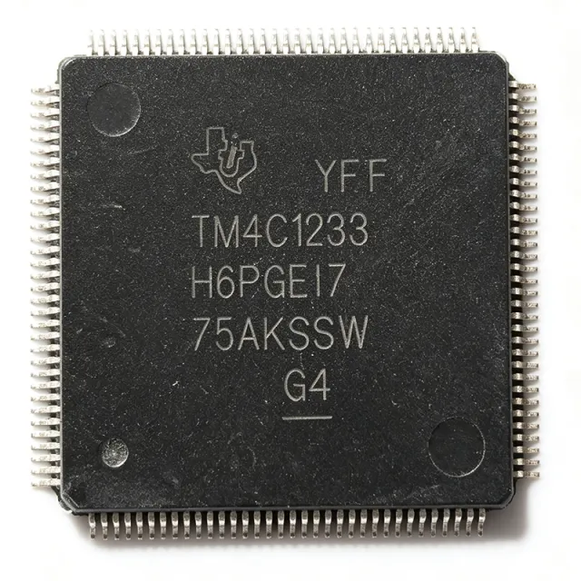
The Texas Instruments TM4C1233H6PGE is a 32-bit Arm Cortex-M4F microcontroller running at 80 MHz with 256 KB flash, 32 KB SRAM, dual CAN 2.0 controllers, RTC, and USB device support, housed in a 144-pin LQFP (20x20 mm) package. A microcontroller unit (MCU) is a single-chip computer that integrates a processor core, memory, and peripherals on one die. Within the semiconductor hierarchy, the TM4C1233H6PGE belongs to the 32-bit embedded microcontroller class, part of the Tiva C Series TM4C123x family built on the Arm Cortex-M4F architecture, which adds a hardware single-precision FPU, DSP instructions, and a Memory Protection Unit (MPU) on top of the standard Cortex-M core. Key features include the 80 MHz core with integrated FPU and MPU, 256 KB of on-chip flash with in-system programming support, 32 KB of SRAM, and a rich peripheral set: up to two CAN 2.0 controllers, USB 2.0 device, multiple UART, SSI, and I2C modules, 12-bit ADCs, PWM generators, and a battery-backed hibernate module with real-time clock. This combination makes the device well suited to mixed-signal industrial control where deterministic real-time response and robust fieldbus connectivity are required. Technically, the device uses the Tiva C Series 123x platform with a nested vectored interrupt controller (NVIC), SysTick timer, and both a precision internal oscillator and main oscillator inputs. Flash-based memory supports firmware updates via CAN or UART bootloaders, easing field maintenance in deployed equipment. Typical applications cited by TI include remote monitoring, electronic point-of-sale machines, test and measurement equipment, network appliances and switches, factory automation, HVAC and building control, and fire and security systems. A key design consideration is SRAM budgeting: enabling USB stacks and RTOS middleware can consume several kilobytes of the 32 KB SRAM, so applications needing more headroom should evaluate the TM4C123GH6PGE variant or the TM4C129x class. This page synthesizes verified distributor data, drop-in same-family alternatives, pricing, and practical design notes not found in the manufacturer datasheet alone.

USD $7,15 Contacto
TM4C1237H6PZI - 80MHz ARM Cortex-M4F MCU 256KB Flash | TI
TM4C1237H6PZI

TM4C1237H6PZI - 80MHz ARM Cortex-M4F MCU 256KB Flash | TI

The Texas Instruments TM4C1237H6PZI is a 32-bit ARM Cortex-M4F microcontroller running at up to 80 MHz, integrating 256 KB of single-cycle Flash and 32 KB of single-cycle SRAM in a 100-pin LQFP (PZ) package. The part integrates a Floating-Point Unit (FPU) for single-precision IEEE 754 math, a memory protection unit, plus Tiva C Series connectivity peripherals including CAN 2.0, USB 2.0 (full-speed), and a real-time clock (RTC) with Hibernation module. An ARM Cortex-M4F microcontroller is a 32-bit MCU core built around the ARMv7-M architecture with hardware single-precision floating-point support, Thumb-2 instruction set, deterministic interrupt handling (NVIC), and tightly-coupled low-latency memory interfaces. In the broader taxonomy, the Cortex-M4F belongs to: Cortex-M4 -> Cortex-M family -> ARMv7-M processors -> 32-bit MCU -> microcontroller -> embedded processor -> semiconductor. Tiva C Series MCUs sit in TI's general-purpose 32-bit MCU portfolio, alongside MSP432, Sitara, and Hercules safety MCUs. Key features of the TM4C1237H6PZI include 8 UART, 4 SSI/SPI, 4 I2C, 2 CAN, 1 USB, two 12-bit 1-MSPS ADC modules (totaling up to 24 channels), six 64-bit and six 32-bit general-purpose timers, eight PWM outputs, three quadrature encoder interfaces, and a low-pin-count LCD interface on related derivatives. The 80-MHz system clock and single-cycle memory accesses deliver 100 DMIPS of throughput, while the integrated FPU accelerates DSP and control-loop math. Typical applications span industrial remote monitoring, electronic point-of-sale machines, test and measurement equipment, network appliances and switches, factory automation, HVAC and building control, gaming equipment, transportation, and fire/security systems. The combination of CAN and USB makes it a strong fit for industrial gateways; the RTC plus Hibernation module supports battery-backed timekeeping for metering. When designing with this part, ensure the LDO and I/O supply rails are sequenced within the datasheet limits, observe the 100-pin LQFP 1.4 mm thickness for mechanical clearance, and validate that the application's pin multiplexing matches the selected peripheral set.

Cotización Contacto
TM4C123GE6PZT7R - 80MHz ARM Cortex-M4F MCU, 128KB Flash | TI
TM4C123GE6PZT7R

TM4C123GE6PZT7R - 80MHz ARM Cortex-M4F MCU, 128KB Flash | TI

The Texas Instruments TM4C123GE6PZT7R is an ARM Cortex-M4F based Tiva C Series microcontroller running at 80 MHz with a single-cycle Floating Point Unit (FPU), integrating 128 KB of single-cycle Flash and 32 KB of single-cycle SRAM into a 100-pin LQFP package. Its Cortex-M4F core implements the Thumb-2 instruction set, deterministic nested vectored interrupt controller (NVIC), and hardware divide, single-cycle multiply, and saturated math support for DSP-style operations on a microcontroller footprint. The device is built on a 1.2 V internal core with 3.3 V I/O rails. A microcontroller (MCU) is a single-chip computer integrating a CPU core, volatile and non-volatile memory, and a rich set of programmable peripherals intended for embedded control. The Cortex-M4F class sits in the hierarchy: Cortex-M4F -> Cortex-M series -> ARMv7-M architecture -> 32-bit RISC MCU -> embedded processor -> semiconductor device; the FPU suffix denotes the single-precision IEEE 754 floating point unit. TM4C123GE6PZT7R combines CPU, memory, analog, motion-control, and connectivity peripherals into one IC, replacing what historically required a microprocessor plus external peripherals. Key features include 8 UARTs, 4 I2C, 4 SSI/SPI, 2 CAN 2.0B, USB 2.0 Full-Speed Host/Device/OTG, a 12-bit ADC with 1 MSPS and up to 22 analog inputs, two analog comparators, four general-purpose 16/32-bit timers, two watchdog timers, an Hibernation module with RTC, and a PWM block with fault inputs and dead-band generators. Operating voltage spans 3.15 V to 3.63 V with an LDO-derived 1.2 V core; the MCU is qualified for the industrial -40 °C to +85 °C range. Typical applications include industrial remote monitoring, electronic point-of-sale (POS) terminals, test and measurement front-ends, network appliances and switches, factory automation controllers, HVAC and building-control systems, gaming peripherals, motion-control hobby servos, and lighting controllers. Two integrated CAN controllers make it attractive for distributed industrial nodes and automotive body/motor subsystems. Designers should keep the analog and digital supply rails well decoupled with 100 nF ceramic bypass capacitors placed within a few millimeters of each VDD pin, plus a bulk 10 uF near the regulator output. The 100-LQFP (14x14) package thermal resistance theta_JA of around 47 C/W allows full industrial operation without a heatsink; ensure unused debug and JTAG pins are pulled to defined states when not used to avoid floating-input current draw.

Cotización Contacto
TM4C1290NCPDTI3R - Tiva C Series 120MHz ARM Cortex-M4F MCU, 1MB Flash | TI
TM4C1290NCPDTI3R

TM4C1290NCPDTI3R - Tiva C Series 120MHz ARM Cortex-M4F MCU, 1MB Flash | TI

The Texas Instruments TM4C1290NCPDTI3R is a high-performance 32-bit ARM Cortex-M4F microcontroller from TI's Tiva C Series, featuring a 120MHz core with FPU, 1MB Flash, and 256KB SRAM, housed in a 128-pin TQFP (14x14 mm) package. The device integrates extensive connectivity including Ethernet MAC+PHY, USB 2.0, CAN, UART, I2C, and SPI, making it well suited for connected industrial and IoT embedded designs. What is an ARM Cortex-M4F microcontroller? An ARM Cortex-M4F microcontroller is a 32-bit MCU based on the ARM Cortex-M4 processor core with single-precision floating-point unit (FPU), DSP extensions, and a Nested Vectored Interrupt Controller (NVIC). The M4F sits in the Cortex-M family hierarchy above Cortex-M0/M0+ (low-power 8/16-bit class performance) and Cortex-M3 (basic 32-bit), delivering deterministic real-time performance with DSP-class signal processing capability. Microcontrollers occupy the embedded computing tier below microprocessors (MPUs) in the system-on-chip taxonomy, integrating CPU, memory, peripherals, and often connectivity IP into one package. Key features of the TM4C1290NCPDTI3R include: integrated 10/100 Ethernet MAC and PHY, USB 2.0 full-speed host/device/OTG, two CAN 2.0B controllers, eight UARTs, ten I2C, four SSI/SPI, a 12-bit 2MSPS ADC with up to 24 analog inputs, and a hibernation module with RTC. The on-chip memory of 1MB Flash and 256KB single-cycle SRAM supports data-logging buffers, TCP/IP stacks (such as lwIP or TI's own NDK), and real-time control loops without external memory in many designs. The 16-bit CRC engine and AES/DES/SHA crypto accelerators (via the TivaWare library) are commonly leveraged for secured connectivity. Typical applications include industrial Ethernet gateways, PLC modules, networked sensors, building automation controllers, USB host peripherals (printers, scanners, POS terminals), automotive telematics, smart energy and smart grid endpoints, and SCADA remote terminal units (RTUs). The wide 3.3V I/O and integrated PHY reduce external BOM for cost-sensitive connected designs. When designing with this MCU, pay close attention to the TQFP-128 thermal performance at high CPU loading. Validate that the hibernation current budget meets battery-backed RTC requirements, and ensure PCB layout keeps the Ethernet differential pairs length-matched within datasheet tolerances. This page synthesizes distributor pricing, drop-in Tiva C alternatives, and practical design guidance not found in the manufacturer datasheet alone.

Cotización Contacto
TM4C1294NCPDTI3 - 120MHz Cortex-M4F MCU 1MB Flash | TI
TM4C1294NCPDTI3

TM4C1294NCPDTI3 - 120MHz Cortex-M4F MCU 1MB Flash | TI

The Texas Instruments TM4C1294NCPDTI3 is a 32-bit ARM Cortex-M4F microcontroller from the Tiva C Series operating at up to 120 MHz, with 1 MB of flash memory and 256 KB of SRAM, housed in a 128-pin TQFP (14x14 mm) surface-mount package. It integrates an Ethernet MAC with PHY, USB 2.0 Host/Device/OTG, and a rich serial-peripheral set aimed at highly connected IoT designs. A microcontroller (MCU) is a compact integrated circuit that governs specific operations in embedded systems, combining a processor core, memory, and programmable peripherals on a single die. In the product hierarchy, the TM4C1294NCPDTI3 sits within ARM Cortex-M4F core -> Tiva C Series -> TM4C129x family, and it is code-compatible across the Tiva C lineup, letting designers scale designs without rewriting firmware. Key features include the integrated 10/100 Ethernet MAC+PHY for direct network attachment without an external PHY, dual 12-bit ADCs for analog acquisition, and multiple UART, I2C, SPI, and CAN channels. The Cortex-M4F core adds a hardware floating-point unit (FPU), DSP instructions, and a memory protection unit (MPU) for firmware reliability. The industrial temperature grade covers -40C to +85C. Architecturally, the device pairs the 120 MHz M4F pipeline with 256 KB of on-chip SRAM and 1 MB of flash, a JTAG/SWD debug interface, and TI's TivaWare peripheral driver library. The DSP/FPU acceleration enables real-time control loops and digital signal processing without an external co-processor, while the MPU helps isolate critical code regions in safety-conscious firmware architectures. Typical applications include industrial automation nodes, IoT gateways, building automation and smart-grid equipment, networked control systems, and motor control. The integrated Ethernet MAC+PHY removes external components in many designs, cutting BOM cost and board area. Design consideration: decouple all VDD and VDDA pins with low-ESR ceramic capacitors placed close to the package, follow datasheet guidance for the 1.2V core regulator, and exploit low-power sleep modes in energy-sensitive nodes. This page synthesizes distributor pricing, verified drop-in alternatives, and practical design notes not found in the manufacturer datasheet.

Cotización Contacto
TM4E1231H6ZRBI - Tiva C ARM Cortex-M4 MCU 80MHz 256KB BGA | Texas Instruments
TM4E1231H6ZRBI

TM4E1231H6ZRBI - Tiva C ARM Cortex-M4 MCU 80MHz 256KB BGA | Texas Instruments

The Texas Instruments TM4E1231H6ZRBI is a 32-bit ARM Cortex-M4F microcontroller from the Tiva C (TM4C) Series featuring an 80 MHz core with Floating Point Unit, 256 KB single-cycle Flash, and 32 KB SRAM, packaged in a 157-ball BGA (ZRB package). The part integrates a high-performance analog comparator, two 12-bit ADC modules, multiple UART/SPI/I2C interfaces, and a full-speed USB 2.0 OTG controller with dedicated DMA, suited for industrial control and connectivity-rich embedded designs. An ARM Cortex-M4F MCU is a 32-bit microcontroller that adds a single-precision IEEE 754 Floating Point Unit and DSP extensions to the standard Cortex-M4 architecture. Within the broader taxonomy, this places it as a microcontroller -> embedded processor -> semiconductor device, the same family that includes Cortex-M0/M0+ low-end parts and Cortex-M7 high-performance parts. The 'F' suffix specifically denotes the FPU which is essential for sensor-fusion math, motor-control PI loops, and digital signal processing without integer-only precision loss. Key features include 256 KB Flash with pre-fetch buffer to minimize instruction stalls, 32 KB SRAM with byte-access arbitration, two 12-bit ADC modules each supporting up to 1 MSPS with 12 analog input channels, two CAN 2.0 A/B controllers, a USB OTG full-speed controller with ULPI option, an Ethernet MAC with 1588 timestamp support, and an integrated hibernation module for ultra-low-power battery-backed operation drawing as little as 1.6 uA on VBAT. Architecturally the TM4E1231H6ZRBI uses the Tiva C Series design philosophy combining ARM Cortex-M4F processing with a peripheral-rich pin mux that allows nearly every GPIO to map to alternate functions such as timers, QEI, PWM, and serial interfaces. The device is manufactured on a mature 65 nm process that delivers predictable MHz/mW ratios and supports industrial-grade temperature ranges. Typical applications include industrial motion control, USB-connected human-interface devices, building automation gateways, and factory sensor hubs. The combination of CAN 2.0B, Ethernet, and USB makes the part a strong fit for industrial IoT edge nodes that must bridge legacy field buses with TCP/IP networks. When designing with this device, pay close attention to the BGA157 substrate and use at least 4-layer PCB stack-up with microvia or via-in-pad technology to escape the dense ball grid. Allocate decoupling capacitance directly under the BGA to suppress switching transients during high-speed serial bursts. This page synthesizes current distributor pricing, BGA157 drop-in equivalents, and practical PCB layout guidance not found in the manufacturer datasheet.

Cotización Contacto
TM4E123GH6ZRBI7 - 80MHz ARM Cortex-M4F MCU, 256KB Flash | TI
TM4E123GH6ZRBI7

TM4E123GH6ZRBI7 - 80MHz ARM Cortex-M4F MCU, 256KB Flash | TI

The Texas Instruments TM4E123GH6ZRBI7 is a 32-bit ARM Cortex-M4F microcontroller from the Tiva C Series with an 80 MHz CPU, 256 KB single-cycle Flash, and 32 KB single-cycle SRAM, packaged in a 157-ball BGA (ZRBI). It includes a floating-point unit, a deterministic interrupt controller, and a rich peripheral set for industrial and consumer embedded applications. Key features include 8 UARTs, 4 I2C modules, 4 SSI/SPI controllers, 2 CAN 2.0 A/B controllers, a 12-bit 2-MSPS ADC with 24 analog inputs, two analog comparators, and a 16-bit PWM timer block with up to 32 PWM outputs. The device operates from 3.3 V (LDO regulation on-chip), supports industrial -40C to +85C temperature ranges, and integrates a JTAG/SWD debug interface. The 157-ball BGA package provides compact routing for high-pin-count designs. The TM4E123GH6ZRBI7 sits within the broader category hierarchy: ARM Cortex-M4F microcontroller -> ARM Cortex-M -> 32-bit microcontroller (MCU) -> microcontroller -> embedded processor -> semiconductor. This taxonomy helps engineers locate the part within the TI ecosystem and competing Cortex-M portfolios from NXP, STMicroelectronics, and Microchip. The architecture combines ARM Cortex-M4F core with TI's peripheral driver library and StellarisWare-compatible APIs. The deterministic interrupt controller provides 7 priority levels with tail chaining, reducing interrupt latency for real-time control. Hardware CRC and a random-number generator support communications protocols requiring data integrity verification. Typical applications include industrial motor control, factory automation, building HVAC, programmable logic controllers (PLCs), sensor aggregation hubs, and human-machine interface (HMI) panels. The 80 MHz core with FPU delivers sufficient throughput for closed-loop PID control while the BGA package suits space-constrained PCB designs with high I/O density. When designing with this part, ensure the BGA's thermal vias are properly stitched to internal ground planes for heat dissipation. Allocate sufficient PCB layers for signal escape routing on the 157-ball array, and use the on-chip LDO regulator mode by tying the VDD25 rail to the internal 2.5 V output. This page synthesizes distributor pricing, drop-in Tiva C Series alternatives, and practical design notes beyond the manufacturer datasheet, giving engineers a single source for selection and sourcing decisions.

Cotización Contacto
TMC2005-JT - 5-Port ARCNET Hub Controller | Microchip
TMC2005-JT

TMC2005-JT - 5-Port ARCNET Hub Controller | Microchip

The Microchip Technology TMC2005-JT is an ARCNET 5-port hub controller with a parallel processor interface, packaged in a 64-lead TQFP measuring 10 mm by 10 mm. The device provides the central node management required to connect multiple ARCNET branches through a hub or repeater, while supporting twisted-pair and other interfaces through compatible external transceivers. According to the manufacturer datasheet, the controller filters timing jitter of ±100 ns at 2.5 Mbit/s through an internal digital phase-locked loop and buffers the received network data. An ARCNET hub controller is an interface IC in the ARCNET networking hierarchy. It sits between a host processor and external network transceivers, manages access to shared ARCNET media, and expands a network whose node count and cable length are constrained by transceiver electrical capacity. The TMC2005 is intended for embedded systems that need structured cabling, industrial networking, building automation, transportation equipment, or legacy factory data networks rather than general-purpose Ethernet connectivity. Verified device features include a 5-port hub arrangement, a parallel interface, support for HYC9088, RS-485, HYC5000/4000/2000, and TTL optical-module interfaces, and the ability to operate three different transceiver types simultaneously. It can also connect multiple TMC2005 devices to expand hub count. Network nodes connected to one hub must still use the same data rate because the controller does not perform data-rate conversion. The internal digital PLL and receive buffer are particularly useful on noisy or long industrial networks where sampling jitter could corrupt frames. This filtering improves the reliability of packet reception without requiring all connected nodes to share one physical medium. The parallel processor interface allows the surrounding microcontroller or host logic to configure the hub, monitor status, and service the network. A typical implementation places the TMC2005 between a host processor and five external transceiver channels, with termination and connector arrangements selected for the installed cable and topology. Power and signal integrity depend on proper transceiver separation, controlled-impedance routing, and grounding. The manufacturer datasheet states that a TTL optical-module interface can be connected alongside other supported transceivers, but all devices in a single network must operate at the same data rate. This page combines verified manufacturer and distributor information with practical context for ARCNET hub design. It distinguishes controller features from external transceiver duties, highlights the 2.5 Mbit/s jitter-filtering example, and identifies the documentation gaps that should be resolved before a PCB or production qualification. The TMC2005-JT is therefore best treated as a specialized networking interface component rather than a general Ethernet controller.

Cotización Contacto