Productos (39.000+)

LM2202N - 230 MHz Video Amplifier System | Texas Instruments
LM2202N

LM2202N - 230 MHz Video Amplifier System | Texas Instruments

The Texas Instruments LM2202N is a 230 MHz video amplifier system intended for high-resolution monochrome and RGB color monitor applications, supplied in a 20-pin through-hole DIP package. It combines the video amplification functions needed in display signal paths within one integrated circuit and is identified by National Semiconductor as a general-purpose video amplifier system. A video amplifier system is an integrated circuit that conditions analog video signals so they can be reproduced reliably by a display or monitor. Its position in the signal chain is between the source of a composite or RGB video waveform and the display driver circuitry. The broad product category can be described as video amplifier, then analog video processing IC, then signal-conditioning integrated circuit, and finally semiconductor. The LM2202N is identified as a 230 MHz video amplifier system in a 20-PDIP package. Its key documented characteristics include video-amplifier functionality, a bandwidth designation of 230 MHz, general-purpose classification, through-hole construction, and a commercial-extended temperature grade. These attributes place it in applications requiring high-speed analog video amplification rather than low-frequency audio amplification or general-purpose logic. The LM2202N was developed for high-resolution monochrome and RGB color monitor systems. This application focus distinguishes it from general-purpose op-amp-based video circuits: the device is organized as a complete video amplifier system rather than as a general comparator or precision analog amplifier. At 230 MHz, it is suited to signal paths where wide video bandwidth is an important consideration. Typical uses include RGB monitor input stages, monochrome display channels, video test equipment, and legacy display electronics in which an analog video signal must be amplified before reaching the next processing stage. Component selection should account for the 20-pin DIP footprint, required bypass and termination components, and the signal amplitude expected at the amplifier input and output. Use the manufacturer pin-description table when assigning PCB connections, and follow the application circuit in the manufacturer datasheet for component values and signal termination. Because the part is a through-hole 20-pin DIP, board layout should preserve the package outline, pin numbering, and adequate clearance around adjacent traces. Confirm operating temperature and supply requirements against the datasheet before production use. This page organizes the LM2202N identity, package information, intended applications, sourcing guidance, and design cautions into one engineering reference. It also separates established device facts from parameters that require confirmation from the controlling manufacturer documentation, helping designers evaluate the IC without confusing it with unrelated video processors, monitors, or display-driver components.

Cotización Contacto
LM224AD - Quad 30V 1.2MHz Op Amp | Texas Instruments
LM224AD

LM224AD - Quad 30V 1.2MHz Op Amp | Texas Instruments

The Texas Instruments LM224AD is a standard general-purpose quad operational amplifier with four high-gain, frequency-compensated amplifiers in a 14-pin SOIC package. Its principal ratings include 1.2 MHz gain-bandwidth product, 0.5 V/µs slew rate, 3 mV offset voltage, operation from ±1.5 V to ±16 V, and a 30 V maximum supply rating. The LM224A family is specified for -25°C to 85°C operation. An operational amplifier, or op amp, is a high-gain differential amplifier whose feedback network determines its behavior. The LM224AD belongs to the general-purpose operational-amplifier family within analog ICs and amplifiers. Four independent amplifiers in one package provide a practical way to implement signal conditioning, buffering, voltage comparison, summing, or instrumentation functions when the required bandwidth and precision remain within the device's published ratings. Key characteristics include four amplifier circuits in one package, a 1.2 MHz gain-bandwidth product, and a 0.5 V/µs slew rate. These figures make the device suitable for low-to-moderate-frequency analog signals rather than high-speed video or precision signal-chain applications. The 3 mV offset-voltage listing is particularly relevant when evaluating DC accuracy, while the wide ±1.5 V to ±16 V supply range supports both single-supply and split-supply arrangements. The LM224A device family uses high-gain, internally frequency-compensated amplifiers. Compensation avoids the need for an external dominant-pole capacitor in typical closed-loop uses, simplifying analog circuit design. Because all four channels share one package, designers can also reduce board area when four similar amplifier functions are required. Single and split supplies are relevant because the same amplifier can support grounded or bipolar signal systems, subject to the published common-mode and output-swing limits. Typical uses include four-channel sensor conditioning, low-frequency active filters, industrial control interfaces, general-purpose signal buffers, comparators with positive feedback, and analog summing networks. In each case, designers should verify noise, input bias current, common-mode range, output swing, stability, and load-driving capability against the manufacturer datasheet because those values are not present in the supplied source data. The primary design consideration is ensuring that signal bandwidth and amplitude remain compatible with the 1.2 MHz bandwidth and 0.5 V/µs slew rate. Place decoupling capacitors close to the supply pins, maintain a quiet ground reference, and route sensitive input signals away from high-current switching nodes. The complete 14-pin pin assignment and published limits should be checked in the manufacturer datasheet before layout release. This page combines the verified LM224A and LM224AD listings with distributor package information, same-package replacement candidates, and practical design guidance. It distinguishes documented ratings from parameters that still require direct confirmation from the official LM224 datasheet, avoiding unsupported assumptions about electrical performance, compliance, or stock status.

Cotización Contacto
LM224ADR - Quad 30V 1.2MHz Op Amp | Texas Instruments (Tape & Reel)
LM224ADR

LM224ADR - Quad 30V 1.2MHz Op Amp | Texas Instruments (Tape & Reel)

The Texas Instruments LM224ADR is a standard general-purpose quad operational amplifier with four high-gain, frequency-compensated amplifiers in a 14-pin SOIC package. Its principal ratings include 1.2 MHz gain-bandwidth product, 0.5 V/µs slew rate, 3 mV offset voltage, operation from ±1.5 V to ±16 V, and a 30 V maximum supply rating. The LM224A family is specified for -25°C to 85°C operation. An operational amplifier, or op amp, is a high-gain differential amplifier whose feedback network determines its behavior. The LM224ADR belongs to the general-purpose operational-amplifier family within analog ICs and amplifiers. Four independent amplifiers in one package provide a practical way to implement signal conditioning, buffering, voltage comparison, summing, or instrumentation functions when the required bandwidth and precision remain within the device's published ratings. Key characteristics include four amplifier circuits in one package, a 1.2 MHz gain-bandwidth product, and a 0.5 V/µs slew rate. These figures make the device suitable for low-to-moderate-frequency analog signals rather than high-speed video or precision signal-chain applications. The 3 mV offset-voltage listing is particularly relevant when evaluating DC accuracy, while the wide ±1.5 V to ±16 V supply range supports both single-supply and split-supply arrangements. The LM224A device family uses high-gain, internally frequency-compensated amplifiers. Compensation avoids the need for an external dominant-pole capacitor in typical closed-loop uses, simplifying analog circuit design. Because all four channels share one package, designers can also reduce board area when four similar amplifier functions are required. Single and split supplies are relevant because the same amplifier can support grounded or bipolar signal systems, subject to the published common-mode and output-swing limits. Typical uses include four-channel sensor conditioning, low-frequency active filters, industrial control interfaces, general-purpose signal buffers, comparators with positive feedback, and analog summing networks. In each case, designers should verify noise, input bias current, common-mode range, output swing, stability, and load-driving capability against the manufacturer datasheet because those values are not present in the supplied source data. The primary design consideration is ensuring that signal bandwidth and amplitude remain compatible with the 1.2 MHz bandwidth and 0.5 V/µs slew rate. Place decoupling capacitors close to the supply pins, maintain a quiet ground reference, and route sensitive input signals away from high-current switching nodes. The complete 14-pin pin assignment and published limits should be checked in the manufacturer datasheet before layout release. This page combines the verified LM224A and LM224ADR listings with distributor package information, same-package replacement candidates, and practical design guidance. It distinguishes documented ratings from parameters that still require direct confirmation from the official LM224 datasheet, avoiding unsupported assumptions about electrical performance, compliance, or stock status.

Cotización Contacto
LM224AN - 30V Quad Op Amp, 1.2MHz | Texas Instruments
LM224AN

LM224AN - 30V Quad Op Amp, 1.2MHz | Texas Instruments

The Texas Instruments LM224AN is a four-channel, internally compensated operational amplifier with a 30 V maximum supply rating, 1.2 MHz unity-gain bandwidth, and 3 mV input offset voltage, housed in a 14-pin PDIP package. It is designed for general-purpose analog signal conditioning from single- or dual-supply circuits. The four independent amplifiers share common supply and ground pins but otherwise provide separate input and output connections. An operational amplifier is a high-gain, analog differential-input amplifier intended for feedback-based signal conditioning. The LM224 belongs to the operational-amplifier hierarchy within analog and linear integrated circuits. Internally compensated amplifiers simplify closed-loop design because no external compensation network is required for ordinary unity-gain or inverting-amplifier configurations. Single-supply operation permits the output to approach ground, while split-supply operation supports bipolar signal processing around a zero-volt reference. The LM224AN provides four amplifiers in one 14-pin PDIP package, helping reduce board area compared with four individual single amplifiers. Its specified unity-gain bandwidth of 1.2 MHz supports moderate-frequency signal conditioning, while internally distributed compensation permits operation without an external frequency-compensation capacitor. The 3 mV offset specification characterizes the input mismatch that can appear as a DC error in high-gain feedback configurations. A 30 V maximum supply rating accommodates higher-voltage industrial and legacy analog systems when operating constraints and dissipation are properly evaluated. The device is suitable for audio tone control, analog signal conditioning, sensor interfaces, control loops, and general instrumentation. Four independent channels allow an instrumentation amplifier, instrumentation signal-conditioning stage, multi-axis sensor interface, or four-channel measurement circuit to use one package. The PDIP package also facilitates prototyping, inspection, and replacement during maintenance because its leads are accessible and compatible with conventional through-hole assembly methods. When designing with the LM224AN, confirm the actual operating supply voltage, load current, input common-mode range, output swing, and thermal dissipation under worst-case conditions. Input and output stability depend on load capacitance and source resistance, so breadboard and long-lead prototypes should be checked with an oscilloscope before production. Decoupling capacitors should be placed close to the supply and ground pins to limit supply ripple and prevent unintended feedback through board parasitics. This page consolidates verified manufacturer and distributor information, same-package drop-in alternatives, specification comparisons, and practical design guidance. It distinguishes documented LM224AN facts from parameters that still require confirmation from the manufacturer datasheet, helping engineers evaluate replacements without treating every electrically similar amplifier as a guaranteed drop-in substitute.

Cotización Contacto
LM224D - Quad General-Purpose Op Amp | Texas Instruments
LM224D

LM224D - Quad General-Purpose Op Amp | Texas Instruments

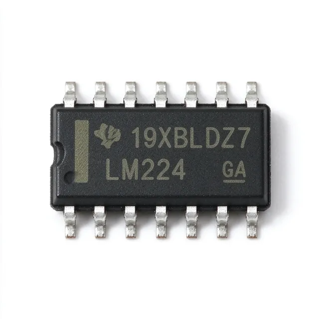
The Texas Instruments LM224D is a standard general-purpose, four-circuit operational amplifier in a 14-SOIC package. The verified distributor result identifies it as a 4-circuit amplifier, while the manufacturer describes the LM224 as a high-performance operational amplifier designed for wide-temperature-range operation. The LM224D combines four independent amplifiers in one package, making it suitable for signal conditioning, instrumentation, sensor interfaces, and industrial control systems. An operational amplifier is an analog signal-processing component that uses high open-loop gain and negative feedback to amplify or process small voltage signals. A quad operational-amplifier package such as the LM224D provides four amplifier sections in one integrated circuit, reducing component count and simplifying PCB layout. Each section can be configured independently as an amplifier, buffer, comparator, or active filter, subject to the device's operating and common-mode limits. The LM224 family is intended for general-purpose analog designs rather than precision or high-speed signal paths. The verified sources specifically identify wide-temperature-range operation and broad supply-voltage capability, making the device relevant to industrial, instrumentation, and test-equipment applications. The 14-SOIC package is a standard surface-mount package with widely used lead spacing, but the exact pin names and electrical limits must be taken from the manufacturer datasheet before final PCB release. The LM224D is useful in low-frequency control loops, sensor conditioning, transducer interfaces, current-voltage conversion, and general instrumentation. Because the available verified data does not state the complete output-current capability, input-bias current, gain-bandwidth product, common-mode range, or exact temperature limits, those values are intentionally not inferred here. The design should account for the amplifier's supply voltage, output swing, input offset, noise, and stability requirements. For PCB implementation, place the device close to the signals it processes and provide adequate bypassing on the supply pins. Decoupling capacitors should be placed at the power-entry points, with short return paths and careful treatment of analog ground versus power ground. Avoid using the LM224D for high-frequency signal chains unless the complete datasheet confirms the required bandwidth and settling behavior. This page combines the verified manufacturer and distributor identity, package information, application context, and engineering guidance. It intentionally separates confirmed data from parameters requiring datasheet confirmation, helping engineers identify the LM224D quickly while avoiding unsupported assumptions.

Cotización Contacto
LM224DG - 4-Channel 1 MHz Op Amp | onsemi | Industrial Control
LM224DG

LM224DG - 4-Channel 1 MHz Op Amp | onsemi | Industrial Control

The onsemi LM224DG is a four-channel general-purpose operational amplifier with true differential inputs, a 1 MHz gain-bandwidth product, and a 14-pin SOIC package. It operates from 3 V to 32 V and supports single-supply or split-supply operation, making it suitable for industrial control, instrumentation, sensor interfaces, and test equipment. The device combines four amplifiers in one package to reduce board area and simplify multi-channel designs. An operational amplifier is a high-gain differential-input amplifier commonly used to buffer sensors, amplify small signals, implement active filters, and drive higher-impedance loads. The LM224 belongs to the operational-amplifier hierarchy, which includes voltage-feedback amplifiers and is used within analog signal-chain and power-management systems. Its four channels can be used independently when the required circuit functions do not interfere. Key verified features include four amplifier circuits, a 1 MHz gain-bandwidth product, a 3 V to 32 V operating supply range, true differential inputs, and a minimum common-mode rejection ratio of 70 dB. The listed input-offset voltage is 5 mV. These characteristics make the LM224DG appropriate for general-purpose signal conditioning where a wide supply range and multiple analog channels are more important than precision or low-noise performance. The LM224 series is designed for low-cost, general-purpose applications and supports operation from a single power supply or split supplies. This flexibility allows engineers to interface signals around ground or operate from an industrial supply without requiring negative rails. Its internal frequency compensation simplifies closed-loop amplifier design, although stable operation still depends on suitable feedback networks and load conditions described by the manufacturer. Typical applications include sensor-signal conditioning, current-loop measurement, industrial process-control modules, data-acquisition systems, and general test equipment. The 14-pin SOIC package is also convenient for through-hole assembly and conventional hand-soldering. Because the LM224 is a general-purpose amplifier, precision instrumentation may require careful offset, bias-current, noise, and common-mode analysis before finalizing the signal chain. When designing around the LM224DG, verify input and output voltage limits for the selected dual or single supply, check that connected loads remain within the amplifier's drive capability, and reserve suitable bypass capacitance close to the supply pins. Stable feedback and compensation arrangements should be copied from the manufacturer datasheet rather than copied blindly from unrelated op-amp circuits. This page combines the verified distributor and manufacturer-linked information for LM224DG with same-package drop-in alternatives, comparison parameters, and practical selection guidance. It highlights where the LM224's wide supply range and four-channel integration are useful, while making uncertainty in unavailable electrical details explicit.

Cotización Contacto
LM224DR - Quad General-Purpose Op Amp | Texas Instruments (Tape & Reel)
LM224DR

LM224DR - Quad General-Purpose Op Amp | Texas Instruments (Tape & Reel)

The Texas Instruments LM224DR is a standard general-purpose, four-circuit operational amplifier in a 14-SOIC package. The verified distributor result identifies it as a 4-circuit amplifier, while the manufacturer describes the LM224 as a high-performance operational amplifier designed for wide-temperature-range operation. The LM224DR combines four independent amplifiers in one package, making it suitable for signal conditioning, instrumentation, sensor interfaces, and industrial control systems. An operational amplifier is an analog signal-processing component that uses high open-loop gain and negative feedback to amplify or process small voltage signals. A quad operational-amplifier package such as the LM224DR provides four amplifier sections in one integrated circuit, reducing component count and simplifying PCB layout. Each section can be configured independently as an amplifier, buffer, comparator, or active filter, subject to the device's operating and common-mode limits. The LM224 family is intended for general-purpose analog designs rather than precision or high-speed signal paths. The verified sources specifically identify wide-temperature-range operation and broad supply-voltage capability, making the device relevant to industrial, instrumentation, and test-equipment applications. The 14-SOIC package is a standard surface-mount package with widely used lead spacing, but the exact pin names and electrical limits must be taken from the manufacturer datasheet before final PCB release. The LM224DR is useful in low-frequency control loops, sensor conditioning, transducer interfaces, current-voltage conversion, and general instrumentation. Because the available verified data does not state the complete output-current capability, input-bias current, gain-bandwidth product, common-mode range, or exact temperature limits, those values are intentionally not inferred here. The design should account for the amplifier's supply voltage, output swing, input offset, noise, and stability requirements. For PCB implementation, place the device close to the signals it processes and provide adequate bypassing on the supply pins. Decoupling capacitors should be placed at the power-entry points, with short return paths and careful treatment of analog ground versus power ground. Avoid using the LM224DR for high-frequency signal chains unless the complete datasheet confirms the required bandwidth and settling behavior. This page combines the verified manufacturer and distributor identity, package information, application context, and engineering guidance. It intentionally separates confirmed data from parameters requiring datasheet confirmation, helping engineers identify the LM224DR quickly while avoiding unsupported assumptions.

USD $0,16 En stock
LM224DT - 4-Channel 1.3MHz Op Amp | STMicroelectronics
LM224DT

LM224DT - 4-Channel 1.3MHz Op Amp | STMicroelectronics

STMicroelectronics LM224DT is a general-purpose quad operational amplifier containing four independent, internally frequency-compensated amplifiers with a gain bandwidth product of 1.3 MHz, input offset voltage up to 7 mV, and operation from a single 3 V to 30 V supply in a 14-pin SOIC package. The LM224DT is designed for instrumentation, buffer-amplifier, and general signal-conditioning applications. An operational amplifier is a high-gain differential amplifier whose feedback network determines its closed-loop behavior. The LM224 family belongs to the linear-amplifier hierarchy: operational amplifier, voltage-feedback amplifier, analog signal-conditioning IC, and semiconductor. Its four amplifiers can operate independently, allowing one package to implement multiple filtering, amplification, comparison, or buffering functions while also supporting split-supply operation. Key features include four independent channels, internal frequency compensation, a 1.3 MHz gain bandwidth product, low input bias current, and low power-supply current. The wide 3 V to 30 V operating range permits use with 5 V, 12 V, 15 V, and 24 V supply systems. The device is available in the 14-pin SOIC outline identified by the T packaging suffix. Each channel uses an internally compensated architecture that simplifies closed-loop design without an external frequency-compensation network. Input offset voltage is specified up to 7 mV, while the gain bandwidth product determines how quickly a closed-loop circuit can amplify signals. The amplifiers are intended for general-purpose precision rather than high-speed or high-current applications, making them suitable for slow sensor signals and buffered control systems. Typical uses include industrial sensor interfaces, low-frequency active filters, transducer amplifiers, audio and communication buffers, battery-powered instrumentation, and four-channel process monitoring. A single package can reduce board area when four independent analog channels are required, although thermal management and input common-mode limits remain important when operating from higher supply voltages. Designers should verify input and output common-mode ranges, output swing, supply current, and stability for the intended load using the manufacturer datasheet. Input and output decoupling should be placed close to the supply pins, and unused amplifier inputs should be biased to a defined common-mode voltage to prevent unstable operation. This page combines verified distributor and manufacturer information, pin-level guidance, practical application notes, and drop-in replacement analysis. It also distinguishes electrically compatible replacements from merely similar amplifiers, helping engineers choose a replacement by package, pinout, supply range, bandwidth, and system requirements.

Cotización Contacto
LM224J - 1MHz Quad 32V Op Amp | Texas Instruments
LM224J

LM224J - 1MHz Quad 32V Op Amp | Texas Instruments

The Texas Instruments LM224J is a general-purpose, internally frequency-compensated quad operational amplifier rated for 32 V operation, with a 1 MHz gain-bandwidth product and 0.5 V/µs slew rate. The device contains four amplifiers in a 14-pin CDIP package, and distributor results identify the orderable LM224J as a tube-packaged, military-temperature variant. An operational amplifier is an analog integrated circuit that uses high open-loop gain to amplify voltage differences. The LM224 belongs to the voltage-feedback operational-amplifier hierarchy and can support closed-loop signal conditioning, sensing, buffering, and control functions. Internally frequency compensation removes the need for an external compensation network in common non-inverting and inverting amplifier configurations. Key features include four independent amplifier sections, support for single or split supplies, a 1 MHz gain-bandwidth product, and a 0.5 V/µs slew rate. The verified distributor result describes a 32 V maximum supply-related rating, while another result reports operating from approximately ±1.5 V to ±16 V. These ranges describe complementary supply arrangements rather than conflicting absolute limits. Technically, the LM224J uses a voltage-feedback architecture intended for general-purpose low-frequency signal paths. Its four channels provide useful channel density for multi-axis sensing, multi-channel conditioning, instrumentation, and embedded control. Because the verified results do not provide complete rail-to-rail, input-bias-current, offset-voltage, noise, or common-mode data, engineers should consult the official LM224 datasheet before setting precision or current-budget limits. Typical uses include transducer buffering, temperature-signal conditioning, low-frequency filtering, industrial control, test equipment, and four-channel sensor interfaces. The 14-CDIP package favors through-hole industrial or legacy-style assemblies rather than compact surface-mount production. Design with adequate output-current margin, stable feedback compensation for the selected gain and load, and supply-bypass capacitors placed close to the package. Check all electrical limits against the official datasheet, especially when using long feedback traces, high-value resistors, or low-noise sensor interfaces. This page consolidates distributor availability, verified package and performance details, practical circuit guidance, and replacement analysis that are not presented together in the manufacturer product-page snippet.

Cotización Contacto
LM224J4 - Quad 1MHz Operational Amplifier | Texas Instruments
LM224J4

LM224J4 - Quad 1MHz Operational Amplifier | Texas Instruments

Texas Instruments LM224J4 is a four-circuit, general-purpose operational amplifier in a 14-CDIP through-hole package, with a 1 MHz gain-bandwidth product and 0.5 V/µs slew rate. The four amplifiers are internally frequency compensated and designed for general-purpose analog signal conditioning from a single power supply. The LM224 family is recognized for its wide operating-temperature capability and straightforward through-hole footprint. An operational amplifier is a high-gain analog building block that compares two input voltages and amplifies their difference. The LM224J4 belongs to the operational-amplifier hierarchy, which includes voltage-feedback amplifiers, analog signal-conditioning ICs, and broader analog semiconductors. Internally compensated amplifiers simplify closed-loop design because the compensation network is integrated rather than added externally. The main features of the LM224J4 are its four independent amplifier sections, 1 MHz gain-bandwidth product, 0.5 V/µs slew rate, and internally compensated operation. These characteristics make it appropriate for low-to-moderate frequency signal paths where straightforward voltage feedback, buffering, amplification, and analog comparisons are needed. The 14-CDIP package also provides a through-hole format that is convenient for prototyping, educational equipment, legacy control systems, and industrial maintenance boards. Each amplifier section provides separate input and output pins, while the IC also exposes shared supply connections. Using multiple amplifiers within one package can reduce board area compared with four separate single-amplifier ICs. The tradeoff is that a fault or excessive power dissipation affecting one section can also affect the shared package, so the complete circuit must be evaluated for supply-current and thermal-budget requirements. Typical uses include industrial sensor conditioning, low-frequency control loops, current-to-voltage conversion, transducer amplification, audio preamplification, and general-purpose laboratory interfaces. The LM224J4 is particularly useful where a 1 MHz bandwidth is sufficient but a high-speed op amp would add unnecessary cost, complexity, or switching-related demands. For a new through-hole design, verify the full ordering code, package drawing, supply limits, output-current behavior, input-common-mode range, and temperature grade against the manufacturer datasheet. Decoupling capacitors should be placed close to the supply pins, and unused amplifier sections should be configured according to the manufacturer guidance rather than left floating. This page combines verified distributor and manufacturer information with package, purchasing, comparison, and practical design guidance. It also distinguishes the LM224J4 from related amplifier and temperature-grade options so engineers can identify a genuine same-package replacement before committing a PCB revision.

Cotización Contacto
LM224KAN - Quad Operational Amplifier | Texas Instruments
LM224KAN

LM224KAN - Quad Operational Amplifier | Texas Instruments

The Texas Instruments LM224KAN is a standard general-purpose quadruple operational amplifier in a 14-pin PDIP package. It contains four independent, high-gain, internally frequency-compensated amplifiers designed to operate from a single supply or split supply over a wide voltage range. The device is intended for instrumentation, buffering, signal-conditioning, and general analog applications where a low-cost, temperature-tolerant amplifier is required. An operational amplifier is an analog building block that uses very high open-loop gain to amplify the difference between its inverting and non-inverting inputs. The LM224 family combines four amplifiers in one package, reducing board area and simplifying multi-channel designs. The device can support single-supply operation as well as positive and negative supply rails, which makes it useful in industrial control, instrumentation, test equipment, and sensor-interface circuits. The LM224KAN is specified for a 14-pin PDIP package and an operating temperature range of -25 °C to 85 °C. The verified product description identifies four amplifier circuits, a standard general-purpose amplifier configuration, and instrumentation or buffer-amplifier use. The LM224 family is associated with the next-generation LM324B and LM2902B families, whose B versions are described as drop-in replacements for earlier LM224, LM324, and LM2902 versions. Key application benefits include four amplifiers in one package, internal frequency compensation, operation from a single supply or split supply, and suitability for instrumentation and buffering. Because the LM224 is a conventional general-purpose amplifier rather than a precision or high-speed device, designers should account for its input offset voltage, input bias current, bandwidth, and output-current limitations when planning signal chains. The internal compensation also means that closed-loop stability is determined primarily by the feedback network and selected gain. Typical uses include sensor signal conditioning, low-level analog measurement, current-to-voltage conversion, audio and communications support circuitry, process-control modules, and educational or laboratory instrumentation. In a single-supply circuit, the input and output signal levels must remain within the amplifier's common-mode and output-swing limits; in a split-supply circuit, the positive and negative rails should be connected according to the manufacturer recommendations. For PCB layout, place the bypass capacitors close to the supply pins, keep input and feedback traces short, and avoid routing high-impedance signal lines beneath or beside power and output paths. The DIP package offers generous lead spacing and straightforward prototype insertion, although it occupies more board area than a surface-mount equivalent. This page combines the verified LM224KAN product data with practical design guidance for selecting, comparing, and implementing the part.

Cotización Contacto
LM224KD - Quad 1.2MHz Op Amp, 32V, 14-SOIC | Texas Instruments
LM224KD

LM224KD - Quad 1.2MHz Op Amp, 32V, 14-SOIC | Texas Instruments

Texas Instruments LM224KD is a four-circuit general-purpose operational amplifier with a 1.2 MHz gain-bandwidth product, support for ±16 V or 32 V total supply operation, and a 14-pin SOIC package measuring 0.154 inch, or 3.90 mm, in width. Each of its four independent, high-gain, frequency-compensated amplifiers can operate from a single supply or from split supplies. An operational amplifier is an analog signal-conditioning semiconductor that uses high open-loop gain and negative feedback to amplify small voltage differences. The LM224 belongs to the operational-amplifier, analog-amplifier, and signal-conditioning IC hierarchy. Four amplifiers in one package can support independent gain stages, differential measurements, active filters, sensor conditioning, and general analog signal chains without requiring four separate packages. Key features include four amplifier circuits, a 1.2 MHz gain-bandwidth product, operation across a broad supply-voltage range, and 2 kV ESD protection. The amplifiers are internally frequency compensated, which simplifies the implementation of stable inverting, non-inverting, summing, and feedback-controlled circuits. The 14-SOIC package also provides a familiar leaded footprint for through-hole assembly and conventional surface-mount production. The LM224KD's single-supply capability is particularly useful in systems where a negative rail is unavailable. Its broad supply range permits operation from low-voltage analog systems as well as higher-voltage industrial and instrumentation circuits. Because it is a general-purpose device rather than a low-noise precision amplifier, designers should confirm input offset, input bias current, noise, and output-swing requirements for the specific measurement. Typical applications include sensor-signal conditioning, test and measurement equipment, industrial control interfaces, current-loop signal processing, audio preamplification, and four-channel analog monitoring. The device is also suitable for low-frequency filter stages where the 1.2 MHz bandwidth provides useful signal-path headroom. Design with the input common-mode range and output swing in mind, especially near the supply rails. Decoupling capacitors should be placed close to the supply pins, input and feedback resistors should preserve suitable noise and bias-current balance, and unused amplifier inputs must be tied to a defined potential rather than left floating. This product page combines manufacturer specifications, replacement cross-reference information, package-level guidance, and application-oriented design notes to support faster component selection and PCB implementation.

Cotización Contacto
LM224KN - Quad 1.2 MHz Op Amp, 14-DIP | Texas Instruments
LM224KN

LM224KN - Quad 1.2 MHz Op Amp, 14-DIP | Texas Instruments

The Texas Instruments LM224KN is a quadruple general-purpose operational amplifier containing four independent, high-gain, internally frequency-compensated amplifiers in a 14-pin through-hole DIP package. Each amplifier operates from a single supply or split supply, with a documented operating range of 3 V to 32 V and a gain-bandwidth product of 1.2 MHz. The LM224KN also provides 2 kV ESD protection and a typical input offset voltage of 600 uV. An operational amplifier, or op amp, is an analog building block that amplifies the difference between two input voltages. In open-loop operation, the LM224 uses its high open-loop gain to make very small differential voltages produce a much larger output. Internal frequency compensation makes the amplifier usable as a stable voltage amplifier without external compensation components, while the four independent sections allow one package to implement four separate analog channels. Key features include a 3 V to 32 V supply range, 1.2 MHz gain-bandwidth product, 600 uV typical input offset voltage, 0.8 mA typical supply-current drain, a common-mode input range that includes ground, and high differential input voltage capability. These characteristics suit general-purpose signal conditioning where the input can operate close to the negative supply rail. The 2 kV ESD protection rating improves handling resilience in industrial and instrumentation environments. The LM224 architecture supports single-supply operation, allowing its positive supply pin to connect to the positive rail and its negative supply pin to connect to ground. Its common-mode range extending to ground simplifies sensing of signals referenced to the zero-volt rail without a separate mid-supply bias. As with any wide-input-range amplifier, careful grounding, supply bypassing, and output-load checks remain necessary for accurate results. Typical uses include sensor-amplifier front ends, DC motor and actuator control loops, industrial transducers, instrumentation amplifiers, audio and communications signal conditioning, and low-frequency active filters. The four amplifiers in one DIP package reduce board area and simplify multi-channel designs where identical electrical performance is useful across several sensing or control paths. When designing with the LM224KN, place supply-bypass capacitors close to the power pins and route sensitive input traces away from high-current switching nodes. Because the amplifier supports output currents referenced to ground, verify load and output-swing limits against the selected supply voltage and load resistance in the manufacturer datasheet. This page consolidates verified distributor availability, pin-level package information, drop-in alternatives, comparison parameters, and practical application guidance. It highlights where the LM224KN remains a practical choice and where a lower-offset, lower-noise, or faster amplifier may be the better engineering choice.

Cotización Contacto
LM224M - Quad 32V Op Amp in 14-SOP | onsemi
LM224M

LM224M - Quad 32V Op Amp in 14-SOP | onsemi

The onsemi LM224M is a general-purpose quad operational amplifier packaged in a 14-pin SOP. Each amplifier provides true differential inputs, internal frequency compensation for unity gain, a large DC voltage gain of 100 dB, and a wide 3 V to 32 V power-supply range. The M suffix identifies the 14-SOP package, while the broader LM224 family is intended for operation from 3 V to 32 V. The input common-mode voltage range includes ground, and the output can swing from approximately 0 V to VCC minus 1.5 V. An operational amplifier is an analog signal-processing semiconductor that uses differential feedback to amplify the voltage difference between its two inputs while rejecting common-mode signals. The LM224M belongs to the hierarchy of operational amplifier, analog amplifier, linear integrated circuit, and semiconductor. Its internally compensated architecture allows stable operation as a unity-gain buffer without external frequency-compensation components, simplifying sensor, control, and signal-conditioning circuits. Key features include four amplifiers in one package, true differential inputs, a 100 dB DC voltage gain, unity-gain frequency compensation, and supply operation from 3 V to 32 V. The ground-referenced input range is useful for battery-powered and single-supply systems in which signals remain near zero volts. Output swing ending near VCC minus 1.5 V should be considered when designing logic-level interfaces or driving heavier loads. The LM224M is suitable for general-purpose industrial analog systems operating across a wider temperature range than commercial-grade LM324 variants, although the exact temperature limits and electrical limits must be confirmed from the selected manufacturer datasheet. It can provide input buffering, sensor amplification, error amplification, and low-frequency closed-loop signal conditioning when operated with suitable passive feedback networks. Typical uses include temperature-sensor interfaces, process-control loops, current-sensing amplifiers, low-level transducers, instrumentation, and embedded analog subsystems. In a sensor circuit, the LM224M can amplify a small differential signal while its feedback network sets the closed-loop gain. In a control loop, it can amplify an error voltage while avoiding external compensation components, subject to stability and noise checks in the completed circuit. When designing around the LM224M, keep input and feedback components close to the relevant pins, provide suitable supply bypassing, and verify the input common-mode range under every supply condition. Avoid assuming rail-to-rail input or output capability. The documented input range includes ground, but does not necessarily extend to the positive supply rail. Likewise, the maximum output swing is not equal to the positive rail because the specified upper limit is approximately VCC minus 1.5 V. This product page synthesizes the verified LM224M package, supply-range, gain, compensation, input-range, and output-swing information with practical design guidance and source traceability. The included comparisons and alternatives are limited to parts that can be evaluated as same-package drop-in options; verify pinout, electrical limits, temperature range, and production status before substitution.

Cotización Contacto
LM224N - Quad 32V 1.2MHz Op Amp | Texas Instruments
LM224N

LM224N - Quad 32V 1.2MHz Op Amp | Texas Instruments

The Texas Instruments LM224N is a quad operational amplifier with a 32 V supply rating, 1.2 MHz gain-bandwidth product, four amplifier circuits, and a 14-pin PDIP package. Designed for general-purpose signal conditioning, the LM224N supports single-supply operation and is positioned for applications requiring multiple amplifiers on one package. According to the TI product page, the LM224-N family is a general-purpose quad amplifier solution. An operational amplifier is an analog building block that uses high open-loop gain to amplify the difference between two input voltages. LM224 devices contain four independently usable amplifiers, allowing one package to implement sensing, buffering, amplification, filtering, or control functions. The LM224N family is commonly associated with single- and dual-supply operation, making it relevant to industrial control, instrumentation, sensor interfaces, and low-frequency analog signal chains. The LM224N combines four amplifiers, a 32 V maximum supply rating, and a 1.2 MHz bandwidth in one 14-pin PDIP package. The verified distributor listing identifies the device as a standard general-purpose amplifier with four circuits and a 14-PDIP package. Its quad configuration can reduce component count and board area in designs that need several similar amplifier stages. The LM224N is intended for general-purpose analog applications where a conventional high-voltage-capable op amp is appropriate. Its internally compensated architecture makes it useful for non-inverting and inverting amplifier stages, voltage followers, comparators, and basic active-filter stages when the circuit requirements fall within the datasheet limits. The package and electrical details should be checked against the selected manufacturer datasheet before layout release. Typical applications include sensor signal conditioning, industrial process monitoring, instrumentation amplifiers, current-voltage conversion, audio and communications support circuits, and embedded control systems. Using four amplifiers in one package is especially useful when several channels need similar conditioning characteristics, such as monitoring multiple sensor inputs. Designers should verify supply voltage, input common-mode range, output swing, offset voltage, slew rate, stability, and temperature limits against the applicable datasheet. Decoupling capacitors should be placed close to the supply pins, and unused amplifier inputs should be configured according to the manufacturer recommendations rather than left floating. This page combines the verified Texas Instruments and distributor data with practical package, application, sourcing, and replacement guidance. It distinguishes confirmed facts from parameters that require verification against the full manufacturer datasheet, helping engineers evaluate the LM224N without relying on assumptions.

Cotización Contacto
LM224NG - Quad 3-32V Op Amp, 14-PDIP | onsemi
LM224NG

LM224NG - Quad 3-32V Op Amp, 14-PDIP | onsemi

The onsemi LM224NG is a quad general-purpose operational amplifier designed for single-supply operation from 3.0 V to 32 V. It contains four true differential-input amplifier sections in a 14-pin PDIP package and is specified for an operating temperature range of -25°C to +85°C. The device is intended for instrumentation, buffering, amplification, and general analog signal-chain applications where a single supply simplifies system power architecture. An operational amplifier, or op amp, is an analog integrated circuit that uses high-gain differential amplification to control an output voltage. The LM224 belongs to the general-purpose op-amp class within the broader voltage-amplifier and signal-conditioning hierarchy. Its four amplifier channels make it useful when a design requires multiple analog functions in one package, reducing board area compared with four separate single or dual amplifier packages. The LM224NG provides a 1 MHz gain-bandwidth product and a slew rate of 0.6 V/µs. These values position the device for low-frequency signal conditioning rather than high-speed pulse or video amplification. The four channels support true differential inputs, allowing common-mode input voltage and input bias current to be considered during sensor-interface and instrumentation design. The listed operating characteristics are suitable for general-purpose amplifier, buffer, and comparator-style circuit arrangements. The 14-pin PDIP package provides through-hole mechanical compatibility and straightforward prototyping. Because the package has no exposed thermal pad, heat dissipation depends on the PCB or socket thermal path and the total dissipation of the four channels. The 3 V to 32 V supply range covers 5 V, 12 V, 24 V, and 32 V rails commonly found in industrial control, consumer electronics, instrumentation, and embedded systems. Single-supply operation also makes zero-crossing and ground-referenced signal conditioning easier to implement. Typical uses include sensor buffering, transducer signal conditioning, low-frequency active filtering, current-to-voltage conversion, test equipment, and control-system analog front ends. Designers should check input common-mode limits, output swing, supply current, stability, and noise requirements for the selected gain and load. The LM224NG is not a precision op amp, so applications requiring very low offset, drift, or noise should compare the device with a higher-accuracy family. This page combines the LM224NG electrical characteristics, package data, sourcing guidance, and application-oriented design notes into a practical engineering reference. Use the manufacturer datasheet for the definitive pin descriptions, maximum ratings, and test conditions before committing the part to a high-voltage or high-reliability design.

Cotización Contacto
LM224PT - Quad 1.3MHz Op Amp | STMicroelectronics
LM224PT

LM224PT - Quad 1.3MHz Op Amp | STMicroelectronics

STMicroelectronics LM224PT is a four-amplifier general-purpose operational-amplifier IC with a 1.3 MHz gain-bandwidth product, 0.4 V/µs slew rate, and 14-TSSOP package. The four amplifiers are independent and internally frequency compensated, allowing each channel to be used separately for signal conditioning, voltage amplification, or analog calculations. The device supports single-supply operation from 3 V to 30 V and split-supply operation up to ±15 V. An operational amplifier is an analog integrated circuit that compares an inverting input with a non-inverting input and drives its output toward the difference between them, multiplied by a very high open-loop gain. In the signal-chain hierarchy, the LM224PT belongs to the operational-amplifier class, then to the broader amplifier IC and analog signal-conditioning categories. Its internally compensated architecture simplifies use in voltage followers, buffers, transimpedance stages, differential amplifiers, comparators, and basic control loops. Key characteristics include four independent amplifiers, a 1.3 MHz gain-bandwidth product, a 0.4 V/µs slew rate, low input bias current, and operation from a broad single supply. These characteristics make the part suitable for industrial control, sensor interfaces, audio preamplification, and low-frequency analog systems. Internal frequency compensation removes the need for an external compensation network in ordinary closed-loop applications. The wide operating-voltage range allows one device family to serve 5 V, 12 V, 15 V, 24 V, and ±15 V systems when the circuit and output-swing limits permit. As a low-power general-purpose amplifier, it prioritizes supply flexibility, moderate bandwidth, and low input bias current rather than rail-to-rail operation, high slew rate, or low-noise precision performance. Designers should check input common-mode range, output swing, input differential voltage, and supply-current limits against the actual circuit. Typical applications include buffering sensor outputs, amplifying low-frequency control signals, conditioning potentiometer inputs, driving analog stages in industrial equipment, and implementing general feedback control. The four-channel configuration can reduce the number of packages in multichannel analog boards while preserving independent operation and grounding flexibility. Layout should keep input and feedback traces short, place input-biasing components close to their pins, and maintain a quiet return path to minimize parasitic pickup. Decoupling capacitors should be placed at the supply pins, while unused amplifier channels should be configured in a stable state rather than left floating. This page combines the manufacturer-device identity, package information, operating characteristics, drop-in replacement research, and application-specific design guidance. It is intended to help engineers evaluate LM224PT quickly, compare it with compatible devices, and implement it correctly without treating a general-purpose amplifier as a precision or rail-to-rail part.

Cotización Contacto
LM239AD - Quad Open-Collector Comparator | Texas Instruments
LM239AD

LM239AD - Quad Open-Collector Comparator | Texas Instruments

Texas Instruments LM239AD is a quad differential comparator in a 14-pin SOIC package, designed for level detection, low-level sensing, memory applications, and general-purpose signal conditioning. The device contains four independent voltage comparators with open-collector outputs. The verified product information identifies the LM239 as a commercial-grade comparator family and the LM239A as a precision quad differential comparator for industrial applications. A comparator is an analog integrated circuit that compares two input voltages and changes its output state when one input becomes higher than the other. Within the semiconductor hierarchy, the LM239AD belongs to the comparator, analog IC, and signal-conditioning categories. Unlike a digital logic gate, the comparator evaluates continuously varying analog voltages and is commonly placed at the boundary between sensors, transducers, reference circuits, and digital control systems. The principal product attributes are four independent comparator channels, differential inputs, open-collector outputs, and a 14-pin SOIC package. Open-collector outputs require an external pull-up resistor to establish a usable high voltage. This arrangement allows the output to be pulled to an external supply, supports wired-AND behavior when multiple comparators share a node, and provides compatibility with TTL, CMOS, and MOS logic when the pull-up voltage and sink-current limits are selected correctly. Each channel compares an inverting input with a non-inverting input. The open-collector transistor pulls the output low when the non-inverting input is below the inverting input and releases the output when that relationship reverses. Because the four sections are independent, they can evaluate different thresholds in one package, reducing component count in multilevel sensing, window-detection, and control systems. The open-collector architecture also prevents the comparator from driving a supply rail directly, which is useful in systems with multiple voltage domains. Typical uses include industrial sensor interfaces, automotive battery and system monitoring, consumer threshold detection, memory-cell sensing, and logic-level translation. In a battery monitor, the comparators can establish several voltage thresholds against an external reference. In a memory system, they can detect charge or voltage levels with minimal external circuitry. Their independent channels also make the device suitable for four-limit or four-zone monitoring where separate comparator decisions are required. Designers should verify the exact input common-mode range, supply-voltage limits, input-offset voltage, response time, output sink current, and electrical characteristics against the manufacturer datasheet before finalizing a design. Place the pull-up resistor close to the output node, maintain the device within its rated common-mode input range, and account for input bias current when using high source impedances. Decoupling and unused-channel handling should follow the device recommendations in the manufacturer documentation. This page combines the LM239AD product identity, comparator operating principle, package information, sourcing guidance, drop-in alternatives, comparison points, and practical application guidance. It is intended to help engineers identify the correct channel count, output architecture, package, and operating limits before integrating the device into analog-control or sensing equipment.

Cotización Contacto
LM239AN - Quad Differential Comparator | STMicroelectronics
LM239AN

LM239AN - Quad Differential Comparator | STMicroelectronics

The STMicroelectronics LM239AN is a low-power quad differential voltage comparator containing four independent comparator channels in a 14-pin through-hole DIP package. The device supports single-supply operation, has a typical input bias current of 25 nA, and belongs to the LM139/LM239 family designed for level detection, low-level sensing, memory, consumer, automotive, and industrial applications. A voltage comparator is an analog semiconductor that compares two input voltages and produces a logic-level output indicating which input is higher. The LM239AN belongs to the hierarchy differential comparator, comparator, analog integrated circuit, and semiconductor. Its four independent channels make it suitable for threshold detection, window monitoring, alarm generation, sensor conditioning, and general digital-interface control. The open-collector outputs can also be used to drive wired logic buses when an appropriate pull-up arrangement is provided. Key characteristics include four independent differential comparators, single-supply operation, a 25 nA typical input bias current, an offset voltage specification as low as 2.0 mV maximum for the LM139 series, and open-collector outputs compatible with CMOS, DTL, ECL, MOS, and TTL according to distributor product information. The 14-DIP package provides through-hole assembly compatibility and ample spacing for inspection and hand soldering. The LM239AN architecture supports independent comparison channels within one package, reducing component count in multi-threshold systems. Because the comparators are independent, their input and output nodes are not internally tied together. Designers must observe the common-mode input range and supply-voltage limits from the manufacturer datasheet, especially when comparing signals that can approach either supply rail. Open-collector outputs require suitable pull-up resistors when a valid high output is required. Typical applications include industrial control systems, automotive sensing interfaces, battery-powered equipment, memory threshold detection, consumer electronics, and precision logic interfaces. Four channels can implement separate overvoltage, undervoltage, temperature, and light-level decisions, while open-collector outputs support alarm aggregation or level translation. Low input bias current is particularly useful when the comparator is driven by high-impedance sensors. When laying out a circuit, keep sensitive input traces away from switching nodes and connect each comparator's supply and ground pins with short, low-impedance paths. Confirm input polarity, common-mode limits, output pull-up values, and input-overvoltage conditions against the manufacturer datasheet before releasing a production design. A single supply is convenient, but dual-supply operation may also be possible within specified limits. This product guide combines device specifications, pin assignments, practical application guidance, and drop-in replacement information to accelerate engineering review. It also highlights the electrical and qualification checks required when substituting another quad comparator on an existing 14-DIP PCB.

Cotización Contacto
LM239D - Quad Open-Collector Comparator, 14-SOIC | Texas Instruments
LM239D

LM239D - Quad Open-Collector Comparator, 14-SOIC | Texas Instruments

The Texas Instruments LM239D is a quad open-collector differential comparator IC with four independent precision voltage comparators, a ±15 V or 30 V supply capability, and a 14-pin SOIC package. The verified product data identifies it as a general-purpose comparator intended for level detection, low-level sensing, and memory applications across consumer, automotive, and industrial equipment. Its low-power architecture and open-collector outputs make it useful where multiple comparator channels must interface with pull-up-based logic systems. What is a voltage comparator? A comparator is an analog interface IC that compares two input voltages and changes its output state according to their relationship. The LM239 belongs to the comparator hierarchy: voltage comparator → differential comparator → quad analog comparator → semiconductor. Each channel is independent, allowing one package to perform four separate sensing or threshold decisions. An open-collector output can sink current while remaining electrically disconnected from the positive supply, requiring an external pull-up when a logic-high output is needed. Key verified features include single or split-supply operation, low input bias current of 25 nA typical, and low input offset current of ±5.0 nA typical. The device supports TTL, MOS, CMOS, DTL, and ECL-compatible outputs. The manufacturer’s related LM239 family page identifies the B-version family as a drop-in replacement for LM239, LM339, and LM2901 families, while also noting improved offset voltage, supply current, propagation delay, and ESD performance for the B versions. The LM239D is appropriate for industrial threshold detection, battery monitoring, sensor signal conditioning, window comparators, control loops, and embedded logic interfaces. In a single-supply circuit, the common-mode input range includes ground, which is useful for low-voltage sensing. In split-supply operation, the differential input range can extend up to the maximum-rated supply span, but the complete electrical limits must be taken from the manufacturer datasheet before final design sign-off. The principal design consideration is output polarity and pull-up implementation. Because the outputs are open collector, four external or shared pull-up networks may be required, and their resistor values determine rise time, power dissipation, and compatibility with downstream logic. Input protection, supply bypassing, and unused-channel handling should also follow the datasheet guidance. This page combines verified product specifications, sourcing information, application guidance, and explicitly qualified replacement analysis for LM239D engineers.

Cotización Contacto
LM239DR - Quad Open-Collector Comparator, 14-SOIC | Texas Instruments (Tape & Reel)
LM239DR

LM239DR - Quad Open-Collector Comparator, 14-SOIC | Texas Instruments (Tape & Reel)

The Texas Instruments LM239DR is a quad open-collector differential comparator IC with four independent precision voltage comparators, a ±15 V or 30 V supply capability, and a 14-pin SOIC package. The verified product data identifies it as a general-purpose comparator intended for level detection, low-level sensing, and memory applications across consumer, automotive, and industrial equipment. Its low-power architecture and open-collector outputs make it useful where multiple comparator channels must interface with pull-up-based logic systems. What is a voltage comparator? A comparator is an analog interface IC that compares two input voltages and changes its output state according to their relationship. The LM239 belongs to the comparator hierarchy: voltage comparator → differential comparator → quad analog comparator → semiconductor. Each channel is independent, allowing one package to perform four separate sensing or threshold decisions. An open-collector output can sink current while remaining electrically disconnected from the positive supply, requiring an external pull-up when a logic-high output is needed. Key verified features include single or split-supply operation, low input bias current of 25 nA typical, and low input offset current of ±5.0 nA typical. The device supports TTL, MOS, CMOS, DTL, and ECL-compatible outputs. The manufacturer’s related LM239 family page identifies the B-version family as a drop-in replacement for LM239, LM339, and LM2901 families, while also noting improved offset voltage, supply current, propagation delay, and ESD performance for the B versions. The LM239DR is appropriate for industrial threshold detection, battery monitoring, sensor signal conditioning, window comparators, control loops, and embedded logic interfaces. In a single-supply circuit, the common-mode input range includes ground, which is useful for low-voltage sensing. In split-supply operation, the differential input range can extend up to the maximum-rated supply span, but the complete electrical limits must be taken from the manufacturer datasheet before final design sign-off. The principal design consideration is output polarity and pull-up implementation. Because the outputs are open collector, four external or shared pull-up networks may be required, and their resistor values determine rise time, power dissipation, and compatibility with downstream logic. Input protection, supply bypassing, and unused-channel handling should also follow the datasheet guidance. This page combines verified product specifications, sourcing information, application guidance, and explicitly qualified replacement analysis for LM239DR engineers.

Cotización Contacto
LM239J - 4-Comparator 1.3us CDIP-14 | Texas Instruments
LM239J

LM239J - 4-Comparator 1.3us CDIP-14 | Texas Instruments

The Texas Instruments LM239J is a quad, general-purpose voltage comparator with four independent channels, a 1.3 microsecond response time, and a 14-pin CDIP package. According to the verified product listings, the device supports a supply range of ±1 V to ±18 V, uses an open-collector output, and is intended for standard analog comparison and threshold-detection circuits. A voltage comparator is an analog signal-processing IC that compares an inverting input with a non-inverting input and changes its output state when the input relationship crosses a selected threshold. The LM239 belongs to the comparator hierarchy and provides four independent channels in one IC, reducing package count when a system needs multiple limit detectors, sorting decisions, or simple control decisions. Its open-collector outputs support wired-AND behavior when suitable pull-up circuitry is provided. Key verified features include four comparators, a response time of 1.3 microseconds, a 2 mV maximum offset-voltage claim in one indexed datasheet listing, and compatibility with CMOS, DTL, ECL, MOS, and TTL output logic according to the verified search results. Another result lists 300 ns response time and 800 microamp supply current for the related comparator family, but these values were not treated as LM239J specifications because the source context is incomplete. The LM239J can operate from single or split supplies, depending on the application and datasheet limits. Because the outputs are open collector, an external pull-up resistor is normally required to establish a valid high output level. The four channels can compare sensor outputs against reference voltages, supervise rails, detect overvoltage or undervoltage conditions, or implement simple oscillator and control functions. Typical designs should account for input common-mode range, output pull-up selection, input filtering, and propagation-delay requirements. In a precision threshold circuit, resistor tolerances and input offset voltage directly affect the switching point. In an industrial control design, lead capacitance and pull-up resistance can affect rise time, while supply bypassing helps reduce noise and unstable switching behavior. This page combines verified manufacturer and distributor information with packaging, application, comparison, and design guidance. It distinguishes confirmed LM239J facts from parameters that were not available in the supplied sources, avoiding unsupported electrical claims or invented pricing.

Cotización Contacto
LM239N - Quad Open-Collector Comparator, 14-DIP | Texas Instruments
LM239N

LM239N - Quad Open-Collector Comparator, 14-DIP | Texas Instruments

The Texas Instruments LM239N is a quad differential voltage comparator with four independent open-collector outputs, a 2 mV maximum offset-voltage specification, and operation from single or split supplies. It is packaged in a 14-pin PDIP and is intended for level detection, low-level sensing, memory applications, consumer equipment, automotive systems, and industrial electronics. The verified TI product page identifies the LM239 family as compatible with TTL, DTL, ECL, MOS, and CMOS logic systems and suitable for sensing close to ground. A voltage comparator is an analog semiconductor that compares two input voltages and changes its output state when the differential input crosses a threshold. The LM239N belongs to the comparator and linear-IC hierarchy, where its low input offset, low input bias current, and common-mode input capability make it useful for analog sensing rather than precision amplification. Its open-collector outputs require an external pull-up resistor when the output must drive a logic node. The four independent channels make the device useful for window detection, threshold crossing, battery monitoring, sensor conditioning, and multiple digital control decisions. TI’s verified material describes operation from 2 V to 36 V DC or split supplies for the related LM139/139A family, while the LM239 listing confirms a wide supply-voltage range and low-power operation. Exact LM239N-specific values not present in the supplied data are retained as required data-needed markers rather than inferred. The open-collector architecture gives the designer control over the pull-up voltage and sink-current budget. A pull-up can be connected to TTL, CMOS, MOS, DTL, or ECL logic as appropriate, but the resistor must satisfy both input-high requirements and the comparator’s output-current limits. This makes the LM239N flexible for mixed-voltage systems where a fixed push-pull output would not be suitable. Typical implementations include overvoltage detection, undervoltage detection, temperature or sensor threshold switches, relay-control logic, industrial control inputs, and consumer battery monitoring. The 14-pin PDIP package is easy to prototype and inspect, although its through-hole form is larger than surface-mount comparator packages. Designers should account for input common-mode limits, output pull-up placement, input noise, unused-channel configuration, and supply bypass capacitors. The key design tip is to treat each comparator channel as an analog input node protected from excessive differential voltage, while using the open-collector output only with a suitable pull-up network. This page combines verified manufacturer and distributor information, explicitly identifies unavailable LM239N-specific data, and separates practical selection guidance from sourced specifications.

Cotización Contacto
LM239NG - Quad 3-36V Comparator | onsemi | DIP-14
LM239NG

LM239NG - Quad 3-36V Comparator | onsemi | DIP-14

onsemi LM239NG is a quad general-purpose CMOS comparator with open-collector outputs, a 3 V to 36 V supply range, and a 14-pin PDIP package. The four independent comparison channels support single-supply or split-supply operation, with typical input bias current of 25 nA and typical input offset current of ±5 nA. Each output uses an open-collector configuration compatible with TTL, CMOS, and MOS logic systems. A comparator is an analog interface integrated circuit that compares two input voltages and produces a logic-level result indicating their relationship. This makes the comparator a member of the comparator hierarchy within amplifier and interface ICs, where it bridges an analog measurement or threshold at the input with digital control or logic at the output. The LM239 family is intended for level detection, low-level sensing, and memory-related threshold functions. The LM239NG provides four comparators in one package, reducing board area and simplifying multi-channel sensing designs. Its low typical input bias current of 25 nA helps preserve the accuracy of high-impedance sensing nodes. A typical input offset voltage of 1.3 mV establishes the practical threshold accuracy near zero, while the typical output saturation voltage of 130 mV at 4 mA supports reliable interfacing with digital logic. The stated operating temperature range is -25°C to +85°C. The open-collector output architecture requires an external pull-up resistor on each channel. This arrangement permits the output voltage to be pulled to the system logic supply rather than being fixed internally, offering flexibility when connecting the device to TTL, CMOS, or MOS logic. Because the output transistor is open, multiple comparators can also share a wired pull-up when their outputs cannot conflict. The design supports both single-supply configurations and split supplies where the input and output reference ranges require additional headroom. Typical uses include detecting voltage thresholds in industrial control systems, monitoring sensor signals in consumer equipment, checking backup and power rails, and evaluating logic levels in memory circuits. The low input bias current is especially useful when a sensing network uses high source impedance. The 14-pin PDIP format is appropriate for through-hole prototypes, educational platforms, and legacy industrial boards where a surface-mount footprint would prevent direct mechanical compatibility. Designers should verify input common-mode limits and output pull-up values for the intended supply configuration. Place the device away from high-current switching paths, connect the ground reference to a low-impedance return, and use the datasheet pin description to preserve the correct channel arrangement. The open-collector pins must not be left without a pull-up when the output is expected to change state. This page combines the LM239NG electrical characteristics, pin assignment, application guidance, and clearly qualified replacement options. It also distinguishes true 14-pin package compatibility from broader functional similarity, helping engineers evaluate replacement decisions before modifying an existing design.

Cotización Contacto