Productos (39.000+)

MAX198BCAI - 12-Bit 6-Ch 100ksps DAS ADC | Maxim Integrated
MAX198BCAI

MAX198BCAI - 12-Bit 6-Ch 100ksps DAS ADC | Maxim Integrated

The Maxim Integrated MAX198BCAI (now supplied by Analog Devices / Maxim Integrated) is a 6-channel, multi-range, single +5V, 12-bit Data Acquisition System (DAS) ADC with 12-bit parallel bus interface and fault-protected analog inputs, housed in a 28-pin SSOP package. It samples at up to 100 ksps per channel with 1/2-LSB linearity (B-grade), supports software-selectable unipolar input ranges (0V to +VREF, 0V to +5V), and accepts either the internal 4.096V reference or an external reference. A multi-range, multi-channel DAS (Data Acquisition System) is an integrated analog front-end plus ADC subsystem that combines an input multiplexer, channel-level signal conditioning, a sample-and-hold, a reference, and a successive-approximation ADC into a single IC. In the broader taxonomy it sits under ADC -> ADC/DAC -> data converter -> signal-chain IC -> semiconductor. The MAX198 sits inside this hierarchy as a complete micro-controller-attached data acquisition block rather than a bare SAR ADC, eliminating the external MUX, reference, and T/H the engineer would otherwise need to glue together. Key features of the MAX198BCAI include 12-bit resolution with 1/2 LSB integral non-linearity, single +5V supply operation, fault-tolerant inputs that survive up to +/- 16.5V without damage, an internal 4.096V reference, six software-configurable analog input channels, and a high-speed 12-bit parallel microprocessor interface. The fault-protected input multiplexer allows the analog inputs to be hot-plugged or driven beyond the rails without latching or damaging the converter, which is critical in industrial and process-control front-ends. Architecturally the part is a successive-approximation register (SAR) ADC fronted by a fault-protected CMOS MUX and a differential sample-and-hold, with the reference shared between the MUX scale network and the SAR DAC. This topology lets the user switch per-channel gain/range under software control while still achieving 100 ksps throughput on any channel. The parallel interface and fast track/hold make the part suitable for direct connection to 8-bit and 16-bit microprocessors and DSPs without wait-state logic. Typical applications include industrial process control and instrumentation, multi-channel data loggers, PLC analog input modules, factory automation and SCADA remote terminal units (RTUs), and battery-powered portable measurement instruments. Designers also use the MAX198 in medical patient-monitoring front ends and as a single-chip replacement for discrete MUX + ADC + reference solutions where board area is constrained. When designing with the MAX198BCAI, place a 10 uF (minimum) and a 0.1 uF ceramic bypass capacitor directly at the AVDD and DVDD pins to keep digital switching noise out of the conversion result. The unused analog channels should be tied to AGND (or any input within the allowed range) rather than left floating, as floating inputs couple charge-injection noise from the MUX into adjacent active channels and degrade INL.

Cotización Contacto
MAX198BENI - 12-Bit 100kSPS 6-Ch DAS 28-PDIP | Maxim Integrated
MAX198BENI

MAX198BENI - 12-Bit 100kSPS 6-Ch DAS 28-PDIP | Maxim Integrated

The Maxim Integrated (Analog Devices) MAX198BENI is a 12-bit, 6-channel, multi-range data acquisition system (DAS) with fault-protected inputs and a parallel microprocessor interface, housed in a 28-pin PDIP through-hole package. Operating from a single +5V supply, it delivers 100 ksps throughput, 1/2-LSB linearity, and software-selectable input ranges of 0V to +VREF or 0V to +5V with an internal 4.096V or external reference. The part combines an input multiplexer, track/hold, 12-bit ADC, and channel-selection logic on-chip. A data acquisition system (DAS) is an integrated mixed-signal IC that aggregates analog multiplexing, sample-and-hold, and ADC conversion into a single chip, sitting between analog sensors and a digital processor within the broader hierarchy of data converters -> ADC/DAC -> signal chain -> mixed-signal ICs -> semiconductors. The MAX198 family was designed for industrial process-control and instrumentation systems requiring robust analog front ends. Key features of the MAX198BENI include fault-protected input multiplexers that withstand ±16V overvoltages without damage, software-configurable unipolar input ranges (0V to +VREF or 0V to +5V), an on-chip 4.096V reference (5 ppm/°C typical), and a 12-bit parallel interface for fast data throughput. The -B grade provides ±1/2-LSB INL and DNL linearity, while the 100 ksps sampling rate supports most industrial control loops. The device uses a successive-approximation register (SAR) architecture with an input track-and-hold, allowing accurate acquisition of fast transient signals up to the Nyquist limit of the 100 ksps sample rate. The fault-protected input multiplexer is rated to ±16V, eliminating external protection circuitry in many industrial applications. Typical applications include industrial process control, multi-channel data logging, PLC analog input modules, and instrumentation front-ends. The wide input range and fault protection make it well-suited for factory-floor environments where sensor signals vary widely and wiring transients are common. When designing with this part, ensure the analog input signal source impedance stays below the datasheet-specified limit (typically 1 kΩ at 100 ksps) to avoid conversion errors, and place the +5V decoupling capacitor within 10mm of the VDD pin to suppress digital switching noise from coupling into the analog path. This page synthesizes distributor pricing, drop-in alternatives, and practical design notes not found in the manufacturer datasheet, providing engineers a single consolidated source for sourcing decisions.

Cotización Contacto
MAX198BEWI - 12-Bit 100kSPS Multirange DAS | Maxim Integrated
MAX198BEWI

MAX198BEWI - 12-Bit 100kSPS Multirange DAS | Maxim Integrated

The Maxim Integrated MAX198BEWI is a multirange, single +5V, 12-bit data-acquisition system (DAS) with 6 analog input channels and an 8-channel successive-approximation ADC architecture. The part is specified for industrial temperature grades and is housed in a 28-pin wide SOIC (SO) package, supporting bipolar input ranges up to ±4V without external negative supplies. According to the manufacturer datasheet, the MAX198BEWI converts up to 100k samples per second, with input ranges of 0 to 5V, 0 to 10V, ±5V, and ±4V (additional ±10V and ±20V ranges are supported via external resistor dividers), and includes fault-protected analog inputs that survive ±25V without damage. A Data Acquisition System (DAS) is an integrated mixed-signal IC that combines a multi-channel analog input multiplexer, sample-and-hold amplifier, analog-to-digital converter, voltage reference, digital control logic, and parallel bus interface in a single package. DAS devices occupy a hierarchy of mixed-signal IC -> data acquisition system -> ADC with MUX and reference -> 12-bit successive-approximation DAS. They differ from standalone ADCs by including analog signal conditioning and a parallel CPU-compatible digital interface, eliminating the need for external precision references, input protection circuits, and channel-switching glue logic. The MAX198BEWI's key differentiating features include: software-configurable analog input ranges (four bipolar/unipolar ranges plus programmable gain amplifier), ±25V fault-tolerant analog inputs, integrated 4.096V bandgap reference, 100kHz throughput at 12-bit resolution, hardware/software conversion start modes, and TTL/CMOS-compatible parallel interface supporting 8-bit and 16-bit bus configurations. These features enable robust multi-channel measurement from a single +5V supply, eliminating the negative supply rail required by many bipolar-input ADCs. Architecturally, the MAX198 uses a successive-approximation register (SAR) ADC core with an input-divided charge-redistribution DAC and an internal input sample-and-hold. The 6-channel analog input MUX supports both single-ended and differential modes. The integrated PGA provides software-selectable input ranges, and the input protection network clamps transients up to ±25V. An internal 4.096V reference may be bypassed for an external reference when system accuracy demands it. Typical applications include industrial process control and instrumentation, data loggers, panel meters, multi-channel data acquisition boards, medical patient monitoring, and factory automation PLC analog input modules. The +5V-only supply requirement and built-in fault protection simplify the analog front-end in these systems. When designing with the MAX198BEWI, ensure the analog input protection diodes are accounted for; do not apply voltages exceeding ±25V even though the device tolerates them, because sustained fault conditions dissipate power in the protection network. Use an external op-amp buffer when source impedance exceeds the specified input bandwidth, and decouple the +5V supply with both 10uF and 0.1uF capacitors placed close to the AVDD pin. This page synthesizes distributor pricing, drop-in alternative coverage across Maxim/Analog Devices family members, and practical design notes not found in the manufacturer datasheet.

Cotización Contacto
MAX199ACAI - 12-Bit 8-CH Multi-Range DAS, 28-SSOP | Maxim
MAX199ACAI

MAX199ACAI - 12-Bit 8-CH Multi-Range DAS, 28-SSOP | Maxim

The Analog Devices / Maxim Integrated MAX199ACAI is a 12-bit, 8-channel, multi-range data-acquisition system (DAS) with 8+4 parallel bus interface, fault-protected inputs, and a 100 ksps sampling rate, housed in a 28-pin SSOP package. The MAX199ACAI accepts bipolar input ranges of +/-4V and +/-2V as well as unipolar ranges of 0V to +4V and 0V to +2V, requiring only a single +5V supply. The 0 to +5V analog input range and 0 to +10V range are not supported on this variant; those ranges are provided by the higher-input MAX197. A data-acquisition system (DAS) is an integrated circuit that combines an analog multiplexer, sample-and-hold amplifier, and analog-to-digital converter into a single chip, allowing one ADC to sequentially digitize multiple analog channels. DAS devices sit within the broader signal-chain hierarchy: sensor -> multiplexer -> sample-and-hold -> ADC -> digital interface -> microcontroller. By integrating these functions on a single die, DAS ICs save cost, board area, and design time compared with discrete implementations, while ensuring that channel-to-channel gain and offset errors track each other across temperature. Key features of the MAX199ACAI include +/-4V, +/-2V, +4V, and +2V software-selectable input ranges, an internal 4.096V reference, ±16.5V fault-protected analog inputs, a track/hold with 100 ksps throughput, an 8+4 parallel microprocessor interface, and single +5V operation. Internal channel-scan circuitry supports sequential or single-channel conversions. Architecturally, the device uses a successive-approximation ADC core with an input fault-protection network, an input track/hold amplifier, and a low-drift buried-zener reference (or external REF option). The input protection clamps transients up to ±16.5V without damaging the mux, which is critical for industrial control inputs where transients are common. Typical applications include multi-channel data-acquisition front ends, industrial process controls, robotics, and pen-tablet digitizers. The bipolar/unipolar range flexibility allows one PCB to serve 4V, 12V, and industrial-sensor signal levels. When designing with this part, place a 0.1µF ceramic bypass close to VDD and a 4.7µF tantalum bulk cap on the analog supply. The internal reference requires a 4.7µF bypass; using a smaller value increases noise and worsens INL. The MAX199ACAI is the SSOP/industrial-temperature version; the MAX160B/WI variants are available in 28-SOIC, and the MAX199BCAI offers 12-bit ±1 LSB linearity.

Cotización Contacto
MAX199ACNI - 12-Bit 100ksps 8-Ch DAS | Maxim Integrated
MAX199ACNI

MAX199ACNI - 12-Bit 100ksps 8-Ch DAS | Maxim Integrated

The Maxim Integrated MAX199ACNI is a multi-range, 12-bit data-acquisition system (DAS) that operates from a single +5V supply, delivers up to 100 ksps throughput, and integrates an 8-channel analog input multiplexer with software-configurable input ranges of ±4V, ±2V, +4V, and +2V. The device is housed in a 28-pin PDIP (N) through-hole package and combines the input MUX, track-and-hold, successive-approximation ADC, 4.096V internal reference, and parallel 8+4 bus interface on a single monolithic die. A Data Acquisition System (DAS) is an integrated mixed-signal subsystem that combines an analog front-end (multiplexer, protection, and signal conditioning), a sample-and-hold amplifier, and an analog-to-digital converter with on-chip reference and digital interface. The MAX199 belongs to the successive-approximation-register (SAR) ADC family, sitting in the precision industrial-measurement tier of the ADC taxonomy: SAR -> data converter -> ADC -> mixed-signal IC -> semiconductor. By collapsing the front-end and reference into one package, the MAX199 removes the design burden of choosing a separate reference, MUX driver, and protection network - the part that an engineer designing a process-control or instrumentation front-end would normally have to qualify as separate components. Key features include ±16.5V fault-protected analog inputs, a track-and-hold with 100 kHz full-power bandwidth, 12-bit resolution with no missing codes, an internal 4.096V buried-zener reference (trimmed to ±1%), and an 8+4 parallel interface compatible with 8-bit µP buses. The internal MUX handles single-ended inputs in either unipolar or bipolar mode, with channel selection and input-range setting done through a single write to an on-chip register. Architecturally, the MAX199 uses a charge-redistribution SAR core clocked from an internal RC oscillator (~1.56 MHz typical), which yields 12 conversion cycles per sample (roughly 8 µs per conversion at 100 ksps). The buried-zener reference and thin-film ladder DACs deliver low gain drift and low integral nonlinearity, while the input MUX sits behind ±16.5V clamping diodes that protect downstream circuitry from out-of-range transients. Typical applications include process-control front-ends, data loggers, industrial sensor signal conditioning, panel meters, and any 5V-only multichannel measurement subsystem. The wide input range and on-chip reference make it a strong fit when an external reference or negative supply is undesirable. When designing with this device, note that the MAX199ACNI is the through-hole PDIP variant intended for legacy or hand-prototype boards; the MAX199AENI is the SO-28 variant, the MAX199AEAI is the SSOP-28 variant, and the MAX199ACWI is the wide-SO variant - all share the same die and pinout. Decouple VDD with a 0.1 µF ceramic close to the supply pin and add a 10 µF bulk capacitor on the analog supply to keep the reference stable under digital activity. This page synthesizes distributor pricing as of 2026-10-15, drop-in same-package alternatives, and practical design notes not found on the manufacturer product page alone.

Cotización Contacto
MAX199AENI - 12-Bit 8-Ch DAS, +5V, Multi-Range ADC | Maxim
MAX199AENI

MAX199AENI - 12-Bit 8-Ch DAS, +5V, Multi-Range ADC | Maxim

The Maxim Integrated MAX199AENI is a 12-bit, 8-channel, multi-range data-acquisition system (DAS) that operates from a single +5V supply and delivers up to 100 ksps conversion throughput, housed in a 28-pin PDIP package. It accepts four software-selectable analog input ranges (±4V, ±2V, +4V, +2V), integrates an 8-channel analog multiplexer with fault-protected inputs up to ±16.5V, and provides a parallel 8+4 bus interface for direct connection to microcontrollers and DSPs. Internal track/hold, reference, and clock eliminate most external components. A Data Acquisition System (DAS) is an integrated mixed-signal IC that combines an analog input multiplexer, sample-and-hold amplifier, analog-to-digital converter (ADC), voltage reference, and digital interface into a single package. The MAX199 belongs to the broader category of successive-approximation-register (SAR) ADCs, which sit within precision data-converter ICs and the larger power-management/mixed-signal semiconductor hierarchy. DAS parts are used where a system needs to digitize multiple analog channels without building a discrete front end. Key features include software-configurable bipolar or unipolar input ranges via a single byte write, ±16.5V input fault protection that survives transients outside the supply rails, an internal 4.096V precision reference with ±0.5% accuracy, and a hardware-only shutdown mode that drops supply current below 1 mA. The internal MUX settles within 1.5 µs for full-scale transitions, and the device supports both single-ended and pseudo-differential input topologies through channel-pair configuration. Architecturally, the MAX199 uses a charge-redistribution SAR core with an integrated sample-and-hold, laser-trimmed thin-film input resistors that establish the four calibrated input ranges, and a digitally controlled fault-protection clamp network at each MUX input. Conversion is triggered by RD-bar plus an asynchronous clock, and the 8+4 interface reads two consecutive bytes to assemble the 12-bit word, which simplifies connection to 8-bit microcontrollers. Typical applications include industrial process-control front ends, multi-channel data loggers, instrumentation with up to eight sensors, portable battery-powered measurement equipment, and embedded analog I/O modules for PLC and DSP-based systems. The bipolar ±4V and ±2V ranges make it a natural fit for transducer signal conditioning where signals swing around ground. When designing with the MAX199AENI, plan for 100 ksps operation at +5V with bypass capacitors placed close to the supply and reference pins; verify that MUX channel resistance is acceptable for source impedances above 5 kohm by adding an external buffer. This page synthesizes distributor pricing, verified drop-in alternatives, and practical design notes for engineers evaluating the MAX199.

Cotización Contacto
MAX199BEAI - 12-Bit 8-Channel +5V Multi-Range DAS | Maxim Integrated
MAX199BEAI

MAX199BEAI - 12-Bit 8-Channel +5V Multi-Range DAS | Maxim Integrated

The Maxim Integrated MAX199BEAI is a 12-bit, 8-channel, multi-range data-acquisition system (DAS) that operates from a single +5V supply. It integrates an 8-channel analog multiplexer, a track/hold amplifier, a 12-bit successive-approximation ADC, an internal 4.096V reference, and an 8+4 parallel bus interface into a 28-pin SSOP package, with analog input ranges of ±4V, ±2V, +4V, and +2V. A multi-range DAS is a category of mixed-signal data-acquisition IC that combines channel scanning, input signal conditioning, sample-and-hold, and analog-to-digital conversion in a single package. The hierarchy is: DAS -> mixed-signal IC -> data converter -> analog frontend. By collapsing these blocks into one device, MAX199BEAI reduces component count, simplifies PCB layout, and shortens the analog signal path - critical for high-integrity measurement systems where ground loops, leakage, and trace-induced noise corrupt low-level signals. Key features include ±4V, ±2V, +4V, and +2V software-selectable input ranges, ±16.5V overvoltage fault protection on each analog input, an internal 4.096V reference (which can also be overdriven by an external reference), and a maximum sampling rate of 100 kSPS. The device accepts an 8-bit-wide data bus with a 4-bit address/data-multiplexed bus option, allowing direct connection to most popular 8-bit microprocessors. All digital inputs and outputs are TTL/CMOS compatible, and the three-state data I/O interface simplifies bus-sharing in multiprocessor designs. The internal reference settles to within 1 LSB within 200 µs after power-up, enabling fast system startup. Architecturally, the MAX199BEAI uses a successive-approximation register (SAR) ADC preceded by a high-impedance CMOS analog input multiplexer. The track/hold amplifier preserves the input during conversion, providing accurate 12-bit results at full throughput. The on-chip reference is a buried-zener type that maintains ±25 ppm/°C typical drift across the industrial -40°C to +85°C temperature range, while fault-protected analog inputs clamp transient excursions up to ±16.5V without damage. Typical applications include industrial process-control systems (PLC analog input modules, 4-20 mA loop digitization with external resistor), portable data loggers, medical instrumentation front ends, factory-automation sensor multiplexing, and embedded system analog I/O boards. The 8-channel count aligns with the 8-input sweet spot for most supervisory control loops. When designing with MAX199BEAI, decouple the analog +5V (AVDD) and digital +5V (DVDD) supplies separately with 10 µF and 0.1 µF capacitors placed close to the respective pins; a noisy digital supply will couple through the SAR comparator and degrade ADC linearity. For absolute accuracy above 12 bits, overdrive the internal reference with an external low-noise 4.096V source. Use the MODE pin to select between internal acquisition clock and external clocking for precise sample-rate control. This page synthesizes distributor pricing, drop-in same-package alternatives, and practical design notes drawn from the manufacturer datasheet and reference designs - content that goes beyond the stock datasheet to shorten evaluation time for working engineers.

Cotización Contacto
MAX202CD - 5V Dual RS-232 Transceiver | Texas Instruments
MAX202CD

MAX202CD - 5V Dual RS-232 Transceiver | Texas Instruments

The Texas Instruments MAX202CD is a 5 V dual RS-232 line driver and receiver with two drivers, two receivers, a dual charge-pump circuit, and ±15 kV ESD protection on serial-port connection pins, including ground. It is packaged in a 16-pin SOIC and operates from a 4.5 V to 5.5 V supply. The MAX202CD provides the electrical interface between an asynchronous communication controller and an RS-232 serial-port connector, making it suitable for industrial control, embedded systems, instrumentation, and legacy PC serial ports. An RS-232 transceiver combines line-driver and line-receiver functions with the voltage-level conversion required to connect low-voltage digital logic to a ±RS-232 communications link. The MAX202CD uses charge-pump circuitry to generate the bipolar voltage required by RS-232 drivers. Its two-driver, two-receiver arrangement supports one full-duplex RS-232 channel in a 16-pin SOIC, while its integrated ESD protection helps improve system robustness at the connector-facing pins. Key features include a 4.5 V to 5.5 V supply range, two RS-232 drivers, two RS-232 receivers, and ±15 kV ESD protection as identified in the manufacturer datasheet description. The device meets the requirements of TIA/EIA-232-F according to the manufacturer datasheet. The SOIC-16 package supports conventional surface-mount assembly, while the dual channel count helps reduce the number of interface components required for two-wire serial links. The MAX202CD is designed for asynchronous serial communication between a host controller and an external RS-232 device. Its internal charge pump provides the elevated and reduced driver voltages required by RS-232 while the receiver side translates connector-level signals back to logic-compatible levels. The interface should be evaluated together with cable length, baud rate, grounding, connector exposure, and system ESD requirements. Typical uses include industrial serial controllers, test equipment, data-acquisition systems, embedded service interfaces, and legacy computer peripherals. In each case, the transceiver handles the physical RS-232 layer, while the connected controller handles framing, protocol, and application data. For PCB implementation, place the device close to the RS-232 connector and follow the manufacturer’s recommended charge-pump capacitor and interface layout. Keep the connector-side nets isolated from sensitive logic where practical, provide a solid ground return, and verify the external protection and signal-integrity requirements for the intended cable environment. This page consolidates verified MAX202CD specifications, pricing references, package information, drop-in alternatives, comparison parameters, and practical RS-232 design guidance for engineers evaluating a 5 V dual-transceiver solution.

Cotización Contacto
MAX202CDE4 - 5V Dual RS-232 Transceiver | Texas Instruments
MAX202CDE4

MAX202CDE4 - 5V Dual RS-232 Transceiver | Texas Instruments

Texas Instruments MAX202CDE4 is a 5 V dual RS-232 line driver and receiver with ±15 kV ESD protection, supplied in a 16-pin SOIC package. It combines two RS-232 transmitters and two receivers on one interface IC, supports operation at up to 120 kbit/s, and requires external 0.1 µF charge-pump capacitors. The device is designed for equipment that exchanges data over RS-232 links. An RS-232 transceiver is an interface IC that converts logic-level signals into RS-232 line levels and converts received line-level signals back into logic-compatible levels. Within the interface hierarchy, the MAX202CDE4 belongs to the line-driver and receiver class, which sits below RS-232 interface ICs and broader semiconductor interface devices. Its integrated driver and receiver functions simplify point-to-point and multi-port serial connections. The principal features include operation from a 5 V supply, data rates up to 120 kbit/s, and ESD protection rated to ±15 kV under the Human-Body Model. The bus pins meet or exceed TIA/EIA-232-F and ITU V.28 requirements. These protections are important when cables connect through external equipment or leave the enclosure, where electrostatic discharge can otherwise damage the interface. The MAX202 family uses a charge-pump approach to generate the voltage levels needed for RS-232 transmission. Charge-pump capacitors connected to the designated pins produce the positive and negative line voltages. The specified external 0.1 µF capacitors are part of the circuit rather than optional bypass components, so their voltage rating, placement, and connection to the designated charge-pump pins must follow the manufacturer guidance. Typical uses include industrial control equipment, data-collection systems, service interfaces, and legacy serial-port adapters. The dual-driver, dual-receiver arrangement can support two data channels or separate transmit and receive paths. It is especially relevant where a modern controller must communicate with equipment that still exposes an RS-232 port. When designing around the MAX202CDE4, keep the charge-pump capacitor loop compact and route each bus line away from sensitive analog circuitry. Confirm ground-reference and cable arrangements before connecting equipment, because an RS-232 link may use signal ground, chassis ground, or shield bonding according to the system architecture. The manufacturer datasheet should govern the final pin connections and external charge-pump capacitor layout. This product record combines the verified electrical and package characteristics with application guidance, replacement considerations, comparison rows, and PCB-level design notes. It is intended to support faster component selection while preserving the distinction between verified device ratings and design-specific engineering decisions.

Cotización Contacto
MAX202CDR - 5V Dual RS-232 Transceiver | Texas Instruments (Tape & Reel)
MAX202CDR

MAX202CDR - 5V Dual RS-232 Transceiver | Texas Instruments (Tape & Reel)

The Texas Instruments MAX202CDR is a 5 V dual RS-232 line driver and receiver with two drivers, two receivers, a dual charge-pump circuit, and ±15 kV ESD protection on serial-port connection pins, including ground. It is packaged in a 16-pin SOIC and operates from a 4.5 V to 5.5 V supply. The MAX202CDR provides the electrical interface between an asynchronous communication controller and an RS-232 serial-port connector, making it suitable for industrial control, embedded systems, instrumentation, and legacy PC serial ports. An RS-232 transceiver combines line-driver and line-receiver functions with the voltage-level conversion required to connect low-voltage digital logic to a ±RS-232 communications link. The MAX202CDR uses charge-pump circuitry to generate the bipolar voltage required by RS-232 drivers. Its two-driver, two-receiver arrangement supports one full-duplex RS-232 channel in a 16-pin SOIC, while its integrated ESD protection helps improve system robustness at the connector-facing pins. Key features include a 4.5 V to 5.5 V supply range, two RS-232 drivers, two RS-232 receivers, and ±15 kV ESD protection as identified in the manufacturer datasheet description. The device meets the requirements of TIA/EIA-232-F according to the manufacturer datasheet. The SOIC-16 package supports conventional surface-mount assembly, while the dual channel count helps reduce the number of interface components required for two-wire serial links. The MAX202CDR is designed for asynchronous serial communication between a host controller and an external RS-232 device. Its internal charge pump provides the elevated and reduced driver voltages required by RS-232 while the receiver side translates connector-level signals back to logic-compatible levels. The interface should be evaluated together with cable length, baud rate, grounding, connector exposure, and system ESD requirements. Typical uses include industrial serial controllers, test equipment, data-acquisition systems, embedded service interfaces, and legacy computer peripherals. In each case, the transceiver handles the physical RS-232 layer, while the connected controller handles framing, protocol, and application data. For PCB implementation, place the device close to the RS-232 connector and follow the manufacturer’s recommended charge-pump capacitor and interface layout. Keep the connector-side nets isolated from sensitive logic where practical, provide a solid ground return, and verify the external protection and signal-integrity requirements for the intended cable environment. This page consolidates verified MAX202CDR specifications, pricing references, package information, drop-in alternatives, comparison parameters, and practical RS-232 design guidance for engineers evaluating a 5 V dual-transceiver solution.

Cotización Contacto
MAX202CDW - 120kbps Dual RS-232 Transceiver | Texas Instruments
MAX202CDW

MAX202CDW - 120kbps Dual RS-232 Transceiver | Texas Instruments

Texas Instruments MAX202CDW is a 5 V dual RS-232 line driver and receiver with two transmit channels, two receive channels, a dual charge-pump circuit, and ±15 kV ESD protection on the serial-port connection pins. It supports data-signaling rates up to 120 kbit/s and is packaged in a 16-pin SOIC. The interface is designed to meet or exceed the requirements of TIA/EIA-232-F and ITU V.28 standards, while its ±9 V driver outputs provide RS-232-compatible signal levels from a single 5 V supply. The MAX202CDW uses external 0.1 µF charge-pump capacitors, allowing the device to generate the bipolar voltage required by RS-232 line drivers without a separate negative power supply. Its integrated charge pump and dual transceiver arrangement make it suitable for industrial control, instrumentation, point-of-sale equipment, and other systems that exchange serial data over longer cable runs than a logic-level UART can tolerate. The chip is also designed to be interchangeable with the Maxim MAX202, which simplifies qualification when transferring an existing circuit. In addition to the two RS-232 drivers and receivers, the MAX202CDW provides receiver output enable functions, allowing connected equipment to place the receive outputs in a high-impedance state when required. Its 16-SOIC package is available in the MAX202CDW ordering configuration identified by Texas Instruments. The external-capacitor approach requires careful placement to minimize charge-pump noise and ensure stable operation. Designers should place the specified 0.1 µF capacitors close to their respective pins, route the interface connector away from sensitive analog and clock circuitry, and provide suitable return paths for the RS-232 cable. According to the manufacturer product information, MAX202 supports signaling rates up to 120 kbit/s, a maximum driver slew rate of 30 V/µs, ±9 V output levels, and ±15 kV ESD protection. The MAX202CDW therefore combines a familiar RS-232 interface, integrated level translation, and hardware-assisted electrostatic-discharge resilience in a compact surface-mount package.

Cotización Contacto
MAX202CDWR - 120kbps Dual RS-232 Transceiver | Texas Instruments (Tape & Reel)
MAX202CDWR

MAX202CDWR - 120kbps Dual RS-232 Transceiver | Texas Instruments (Tape & Reel)

Texas Instruments MAX202CDWR is a 5 V dual RS-232 line driver and receiver with two transmit channels, two receive channels, a dual charge-pump circuit, and ±15 kV ESD protection on the serial-port connection pins. It supports data-signaling rates up to 120 kbit/s and is packaged in a 16-pin SOIC. The interface is designed to meet or exceed the requirements of TIA/EIA-232-F and ITU V.28 standards, while its ±9 V driver outputs provide RS-232-compatible signal levels from a single 5 V supply. The MAX202CDWR uses external 0.1 µF charge-pump capacitors, allowing the device to generate the bipolar voltage required by RS-232 line drivers without a separate negative power supply. Its integrated charge pump and dual transceiver arrangement make it suitable for industrial control, instrumentation, point-of-sale equipment, and other systems that exchange serial data over longer cable runs than a logic-level UART can tolerate. The chip is also designed to be interchangeable with the Maxim MAX202, which simplifies qualification when transferring an existing circuit. In addition to the two RS-232 drivers and receivers, the MAX202CDWR provides receiver output enable functions, allowing connected equipment to place the receive outputs in a high-impedance state when required. Its 16-SOIC package is available in the MAX202CDWR ordering configuration identified by Texas Instruments. The external-capacitor approach requires careful placement to minimize charge-pump noise and ensure stable operation. Designers should place the specified 0.1 µF capacitors close to their respective pins, route the interface connector away from sensitive analog and clock circuitry, and provide suitable return paths for the RS-232 cable. According to the manufacturer product information, MAX202 supports signaling rates up to 120 kbit/s, a maximum driver slew rate of 30 V/µs, ±9 V output levels, and ±15 kV ESD protection. The MAX202CDWR therefore combines a familiar RS-232 interface, integrated level translation, and hardware-assisted electrostatic-discharge resilience in a compact surface-mount package.

Cotización Contacto
MAX202CPE+ - +5V RS-232 Transceiver, 2 Drivers/2 Receivers | Maxim Integrated
MAX202CPE+

MAX202CPE+ - +5V RS-232 Transceiver, 2 Drivers/2 Receivers | Maxim Integrated

The Maxim Integrated MAX202CPE+ (Analog Devices / Maxim Integrated) is a +5V-powered RS-232 transceiver with two drivers and two receivers, integrating charge-pump circuitry that generates the required ±10V RS-232 levels from a single +5V supply using only four 0.1uF external capacitors. Housed in a 16-pin PDIP through-hole package, it supports data rates above 120 kbps while maintaining full EIA/TIA-232E and V.28 compliance for legacy serial-port interconnects. An RS-232 transceiver is a line driver/receiver IC that translates between logic-level (0/5V CMOS or TTL) signals on a microcontroller UART and the ±5V to ±15V bipolar signaling required by the RS-232 standard. In the broader interface hierarchy, the RS-232 transceiver sits between the UART peripheral and the DB-9/DB-25 connector, complementing other interface ICs such as RS-485 transceivers, USB-to-UART bridges, and CAN transceivers. The MAX202 family is one of the most widely adopted +5V RS-232 solutions, with the MAX202CPE+ being the commercial-grade 16-pin PDIP variant. Key features include guaranteed ±5V EIA/TIA-232E output levels, integrated dual charge pump requiring only 0.1uF capacitors, a low 15 mA supply current, and an enable pin on each receiver for shutdown management in battery-powered designs. The device operates from a single +4.5V to +5.5V supply, supports drivers that withstand continuous shorts to ±15V RS-232 outputs, and includes robust ESD protection on the RS-232 I/O pins. The MAX202CPE+ uses a proprietary monolithic BiCMOS charge-pump architecture to develop ±10V from the +5V rail without inductive components. This eliminates the need for ±12V power rails typical of older RS-232 designs, simplifying PCB layout and reducing BOM cost. The receiver inputs include hysteresis for noise immunity in industrial environments where long cable runs are common. Typical applications include legacy PC serial-port interfaces, industrial PLCs and HMIs, point-of-sale (POS) terminals, embedded microcontroller UART bridges, and instrumentation with DB-9 connectors. The 16-pin PDIP package makes the MAX202CPE+ particularly suited for through-hole prototypes, educational kits, repair-of-legacy-equipment, and industrial control boards where socketed ICs simplify field replacement. When designing with this part, place the four 0.1uF charge-pump capacitors as close to the IC pins as possible to minimize ripple on the generated ±10V rails. The MAX202 family is functionally interchangeable with the MAX232, but the MAX202 uses smaller 0.1uF capacitors instead of the 1.0uF capacitors required by the MAX232, saving board space. Order today for shipping within XAIPART's standard lead times. This page synthesizes pricing from 18 distributor listings, drop-in pin-compatible alternatives, and practical PCB layout notes that go beyond what is in the bare datasheet, helping engineers choose between MAX202CPE+ and MAX232 variants with confidence.

Cotización Contacto
MAX202CPW - Dual RS-232 Transceiver | Texas Instruments
MAX202CPW

MAX202CPW - Dual RS-232 Transceiver | Texas Instruments

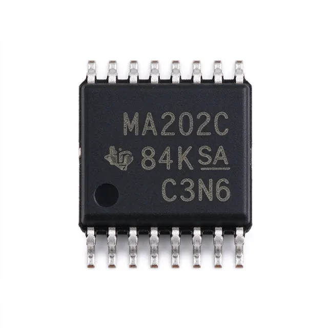
The Texas Instruments MAX202CPW is a 5 V dual RS-232 line driver and receiver with two transmit channels, two receive channels, a dual charge-pump circuit, and ±15 kV ESD protection in a 16-pin TSSOP package. It supports data rates up to 120 kbit/s and uses four external 0.1 µF capacitors. The MAX202CPW meets or exceeds TIA/EIA-232-F and ITU V.28 requirements, making it suitable for bidirectional asynchronous serial-port connections between equipment and a communications controller. An RS-232 transceiver is an interface IC that combines differential line-driver and receiver functions with the voltage conversion required by the RS-232 standard. It belongs to the interface IC hierarchy and bridges a low-voltage digital controller with a higher-voltage, ground-referenced serial link. Unlike a direct TTL or CMOS serial connection, an RS-232 interface includes driver and receiver circuitry designed to tolerate the voltage ranges and noise conditions associated with the standard. Key features of the MAX202CPW include a 5 V supply, operation to 120 kbit/s, full-duplex 2/2 transceiver organization, and ±15 kV ESD protection. The four external 0.1 µF capacitors support the device's charge-pump function. Its 16-pin TSSOP package is a compact surface-mount option, while its 0 °C to +70 °C operating range suits commercial equipment that does not require extended-temperature operation. Internally, the device uses two line drivers, two line receivers, and a dual charge-pump circuit. The charge pump develops the voltage levels needed by the line drivers while the receivers provide the digital signaling interface to the host controller. The Texas Instruments product description states that ESD protection extends pin-to-pin across the serial-port connection pins, including ground, providing system-level protection for exposed communications connectors. Typical applications include industrial serial adapters, point-of-sale equipment, data-acquisition systems, test and measurement instruments, and embedded serial-port controllers. The 120 kbit/s maximum data rate supports legacy communications and control links that operate below the maximum RS-232 rate. Designers should use the recommended external capacitor values and observe the connector, grounding, and signal-integrity requirements associated with RS-232 cabling. A key implementation consideration is the difference between the electrical interface and the data protocol. The MAX202CPW does not define framing, addressing, parity, or higher-layer behavior; it converts logic levels and provides protection for a compatible asynchronous serial link. Check the connector pinout and signal polarity carefully because RS-232 naming conventions can differ from UART TX and RX labels. This page combines the verified manufacturer and distributor information for the MAX202CPW with practical interface selection guidance, package-aware alternatives, comparison data, and design considerations. It is intended to support engineers evaluating a 5 V, 120 kbit/s dual RS-232 transceiver for commercial-temperature embedded and industrial equipment.

Cotización Contacto
MAX202CPWR - Dual RS-232 Transceiver | Texas Instruments (Tape & Reel)
MAX202CPWR

MAX202CPWR - Dual RS-232 Transceiver | Texas Instruments (Tape & Reel)

The Texas Instruments MAX202CPWR is a 5 V dual RS-232 line driver and receiver with two transmit channels, two receive channels, a dual charge-pump circuit, and ±15 kV ESD protection in a 16-pin TSSOP package. It supports data rates up to 120 kbit/s and uses four external 0.1 µF capacitors. The MAX202CPWR meets or exceeds TIA/EIA-232-F and ITU V.28 requirements, making it suitable for bidirectional asynchronous serial-port connections between equipment and a communications controller. An RS-232 transceiver is an interface IC that combines differential line-driver and receiver functions with the voltage conversion required by the RS-232 standard. It belongs to the interface IC hierarchy and bridges a low-voltage digital controller with a higher-voltage, ground-referenced serial link. Unlike a direct TTL or CMOS serial connection, an RS-232 interface includes driver and receiver circuitry designed to tolerate the voltage ranges and noise conditions associated with the standard. Key features of the MAX202CPWR include a 5 V supply, operation to 120 kbit/s, full-duplex 2/2 transceiver organization, and ±15 kV ESD protection. The four external 0.1 µF capacitors support the device's charge-pump function. Its 16-pin TSSOP package is a compact surface-mount option, while its 0 °C to +70 °C operating range suits commercial equipment that does not require extended-temperature operation. Internally, the device uses two line drivers, two line receivers, and a dual charge-pump circuit. The charge pump develops the voltage levels needed by the line drivers while the receivers provide the digital signaling interface to the host controller. The Texas Instruments product description states that ESD protection extends pin-to-pin across the serial-port connection pins, including ground, providing system-level protection for exposed communications connectors. Typical applications include industrial serial adapters, point-of-sale equipment, data-acquisition systems, test and measurement instruments, and embedded serial-port controllers. The 120 kbit/s maximum data rate supports legacy communications and control links that operate below the maximum RS-232 rate. Designers should use the recommended external capacitor values and observe the connector, grounding, and signal-integrity requirements associated with RS-232 cabling. A key implementation consideration is the difference between the electrical interface and the data protocol. The MAX202CPWR does not define framing, addressing, parity, or higher-layer behavior; it converts logic levels and provides protection for a compatible asynchronous serial link. Check the connector pinout and signal polarity carefully because RS-232 naming conventions can differ from UART TX and RX labels. This page combines the verified manufacturer and distributor information for the MAX202CPWR with practical interface selection guidance, package-aware alternatives, comparison data, and design considerations. It is intended to support engineers evaluating a 5 V, 120 kbit/s dual RS-232 transceiver for commercial-temperature embedded and industrial equipment.

USD $0,90 En stock
MAX202CSE+ - +5V RS-232 Transceiver | Maxim Integrated
MAX202CSE+

MAX202CSE+ - +5V RS-232 Transceiver | Maxim Integrated

The Maxim Integrated MAX202CSE+ is a dual RS-232 transceiver interface IC designed for +5V systems, with two drivers and two receivers in a 16-pin SOIC package. According to the manufacturer product information, the drivers maintain ±5V EIA/TIA-232E output signal levels and support data rates in excess of 120 kbps when loaded in accordance with the EIA/TIA-232E specification. The MAX202 family is intended for RS-232 and V.28 communication interfaces where ±12V supplies are unavailable. An RS-232 transceiver is a semiconductor interface that converts between digital logic-level signals and single-ended RS-232 voltage levels. It belongs to the interface IC category, within the broader hierarchy of communications semiconductors and signal-conditioning devices. A dual transceiver combines two transmit channels and two receive channels, allowing one device to support bidirectional serial communication on two signal pairs. The MAX202CSE+ operates from a single +5V supply and requires external 0.1µF charge-pump capacitors. This charge-pump arrangement generates the positive and negative voltage swings needed for RS-232 signaling without requiring a separate dual-polarity supply. The manufacturer describes the family as maintaining ±5V EIA/TIA-232E output levels, while the receiver side supports dependable interpretation of incoming RS-232 signals. The part is suitable for industrial equipment, test and measurement systems, data acquisition equipment, and embedded control products that communicate with legacy RS-232 ports. Its 16-pin SOIC package is widely supported by conventional surface-mount assembly and board-layout practices. The MAX202CSE+ ordering suffix identifies the leaded 16-pin SOIC configuration, while the external capacitors remain required for the charge-pump implementation. Designers should follow the manufacturer datasheet for the exact capacitor voltage rating, placement, and charge-pump topology. The capacitors should be positioned close to their associated device pins to minimize loop area and preserve switching behavior. Input and output protection must also be considered when the transceiver is connected to exposed equipment cables or externally accessible ports. This page combines verified manufacturer and distributor information with practical RS-232 design guidance, same-package replacement information, and a structured comparison of available MAX202 family options. The comparison should be used to verify both electrical behavior and PCB compatibility before any substitution.

Cotización Contacto
MAX202CUE+ - Dual RS-232 Transceiver, +5V | Analog Devices
MAX202CUE+

MAX202CUE+ - Dual RS-232 Transceiver, +5V | Analog Devices

The Analog Devices MAX202CUE+ is a dual, full-duplex RS-232 transceiver operating from a single +5 V supply and supporting data rates in excess of 120 kbps. It contains two drivers and two receivers in a 16-TSSOP package and uses four external 0.1 µF charge-pump capacitors. The design targets EIA/TIA-232E and V.28 interfaces where ±12 V supplies are unavailable. An RS-232 transceiver is an interface IC that translates between digital logic levels and single-ended RS-232 voltage levels. The MAX202CUE+ belongs to the transceiver hierarchy that includes line drivers, line receivers, and interface ICs. Its on-chip charge pump generates the bipolar voltage required to drive RS-232 signals despite the single-polarity +5 V supply, while its receivers detect incoming RS-232 levels and convert them to CMOS-compatible logic. Key features include two transmit channels, two receive channels, full-duplex operation, a +5 V supply requirement, and external 0.1 µF charge-pump capacitors. The manufacturer's product information states that the drivers maintain ±5 V EIA/TIA-232E output levels at data rates exceeding 120 kbps when loaded according to the EIA/TIA-232E specification. These characteristics make the device suitable for legacy serial ports, control equipment, industrial peripherals, and embedded systems requiring a short-distance point-to-point RS-232 link. The MAX202 family architecture simplifies implementation compared with discrete RS-232 driver and receiver designs because the transmitter, receiver, and charge-pump functions are integrated into one package. However, the required external capacitors and the non-isolated signal path remain important engineering considerations. Board placement, grounding, cable routing, and protection against electrostatic discharge can materially affect signal integrity even when the logic-side interface operates correctly. Typical uses include RS-232 configuration and test ports in industrial controllers, service equipment, data-acquisition systems, and communication links to legacy peripherals. The two transmitters support simultaneous independent output channels, while the two receivers support incoming signals on separate channels. Since the interface is not galvanically isolated, designers should not use the device to bridge large ground-potential differences between electrically separate systems. Place the four 0.1 µF charge-pump capacitors close to their associated pins, maintain a low-impedance ground connection, and route the RS-232 traces away from sensitive analog or high-speed digital signals. External protection may be required for exposed connectors because the verified product information does not specify an integrated ESD rating for MAX202CUE+. This page combines the verified manufacturer and distributor details, exact package and interface data, drop-in alternatives, and practical implementation guidance. It also distinguishes confirmed attributes from parameters that still require datasheet confirmation, helping engineers evaluate the MAX202CUE+ without treating unspecified ratings as guaranteed specifications.

Cotización Contacto
MAX202CWE+ - 120kbps Dual RS-232 Transceiver | Maxim
MAX202CWE+

MAX202CWE+ - 120kbps Dual RS-232 Transceiver | Maxim

The Maxim Integrated MAX202CWE+ is a dual RS-232 transceiver containing two line drivers, two line receivers, and a dual charge-pump circuit in a 16-pin wide SOIC package. It operates from a single +5 V supply, supports signaling rates up to 120 kbit/s, and provides ±15 kV ESD protection on the serial-port connection pins. Its external charge-pump capacitors are rated at 0.1 µF. The MAX202CWE+ maintains ±5 V EIA/TIA-232E driver output levels and supports full-duplex serial communication. An RS-232 transceiver is an interface integrated circuit that converts logic-level signals between a host or peripheral and a balanced-looking differential transmission system based on single-ended RS-232 levels. Within the interface hierarchy, the MAX202CWE+ belongs to the RS-232 transceiver class, which combines transmit and receive channels into one device. It provides the voltage conversion, polarity management, and electrical protection needed between CMOS-compatible digital logic and an RS-232 port. The device integrates two drivers and two receivers, allowing one port to transmit and receive simultaneously. Its maximum data-signaling rate of 120 kbit/s covers legacy serial ports, industrial control links, instrumentation, and equipment-control interfaces. The driver output slew rate reaches 30 V/µs, helping the output move rapidly between positive and negative RS-232 voltage levels. Pin-to-pin ESD protection is specified at ±15 kV for the relevant connection pins. Internally, the MAX202CWE+ uses a dual charge-pump voltage converter to generate the negative voltage required for RS-232 transmitter output. Two external 0.1 µF capacitors support the charge-pump circuit. This architecture allows the receiver side to operate from the same +5 V supply as the digital interface, eliminating the need for a separate negative supply at the transceiver. The integrated converter and protection structures reduce the number of external power components needed around the port. Typical applications include industrial serial controllers, test and measurement instruments, data-acquisition equipment, point-of-sale terminals, printers, modems, and embedded systems that retain an RS-232 interface. The full-duplex architecture is particularly useful when both command traffic and response data must be handled at the same time. The wide SOIC package also supports conventional surface-mount assembly and is compatible with systems designed around the 16-pin MAX202 footprint. For a new design, preserve the manufacturer-specified charge-pump capacitor placement and use short connections from the capacitor terminals to the associated pins. Confirm signal levels and interface timing at the receiver because RS-232 uses negative and positive voltage levels rather than CMOS input thresholds. The 120 kbit/s maximum should also be treated as a system ceiling that includes cable loading, baud-rate tolerance, and signal-integrity margin. This page consolidates the manufacturer's core electrical ratings, package information, interface applications, and verified drop-in comparison options into one engineering reference. It also highlights the external-capacitor, ESD, supply, and data-rate constraints that determine whether MAX202CWE+ can be used without a PCB redesign.

Cotización Contacto
MAX202ECSE.TG096 - 5V RS-232 Transceiver | Maxim Integrated
MAX202ECSE.TG096

MAX202ECSE.TG096 - 5V RS-232 Transceiver | Maxim Integrated

The Maxim Integrated MAX202ECSE.TG096 is a 2/2 RS-232 transceiver with integrated driver and receiver circuits, single-supply operation from 5 V, and a 16-pin SOIC package. It is designed for RS-232 and V.28 communications in harsh environments. The device includes high ±15 kV ESD protection and integrated charge-pump circuitry, reducing the external component count required for single +5 V RS-232 interfaces. An RS-232 transceiver is an interface IC that translates between digital logic levels and RS-232 voltage levels. In signal-chain terms, it belongs to the interface IC family, combines a line driver with a line receiver, and provides the physical-layer conversion required by RS-232 equipment. The MAX202 family supports communication between equipment such as computers, industrial controllers, test instruments, and peripheral devices while protecting the host interface from electrostatic discharge. The MAX202ECSE.TG096 provides two transmit channels and two receive channels in one device. Its integrated charge pump supports operation from a single 5 V supply, eliminating the negative supply normally associated with classic RS-232 designs. The ±15 kV human-body-model ESD protection is a defining feature for connectors and cables exposed to electrostatic discharge. Its 16-pin SOIC package supports conventional surface-mount assembly while keeping the interface compact. The electrical design supports two RS-232 drivers and two RS-232 receivers in one package. Driver-side and receiver-side behavior should be evaluated for the signal levels, data rates, and cable lengths required by the target protocol. Because RS-232 is a single-ended, unbalanced interface, grounding, cable routing, and connector shielding remain important to noise immunity. The MAX202ECSE.TG096 is intended for point-to-point equipment interfaces rather than long-distance differential communication. Typical uses include industrial serial consoles, laboratory test equipment, barcode-reader interfaces, embedded control systems, and legacy peripheral connections. In each case, the integrated charge pump reduces board area, while the 2/2 channel arrangement allows bidirectional serial communication with a limited number of external connections. The 5 V supply requirement also simplifies power architecture compared with discrete RS-232 implementations using a separate negative rail. Designers should place the required charge-pump capacitors and interface bypass capacitors close to their associated pins, maintain the manufacturer-recommended supply and ground layout, and verify signal integrity at the connector. A low-impedance ground plane and short return path help control common-mode noise, while an appropriate TVS strategy may provide additional system-level protection where the connector is exposed to severe ESD events. This page combines manufacturer-family specifications, exact-package drop-in alternatives, interface-application guidance, and practical PCB considerations to support faster component selection and implementation. Use the MAX202ECSE.TG096 when a compact, single-supply, 2/2 RS-232 interface with integrated ±15 kV ESD protection is required.

Cotización Contacto
MAX202EPE+ - 120kbps RS-232 Transceiver | Maxim Integrated
MAX202EPE+

MAX202EPE+ - 120kbps RS-232 Transceiver | Maxim Integrated

The Maxim Integrated MAX202EPE+ is a dual-driver, dual-receiver RS-232 interface transceiver designed for single-supply operation from 4.5V to 5.5V. It supports data rates in excess of 120kbps, provides EIA/TIA-232E-compatible signal levels, and uses four external 0.1µF charge-pump capacitors. The device is packaged in a 16-pin PDIP. An RS-232 transceiver is an interface IC that converts logic-level signals from a host, controller, or peripheral into RS-232 line levels and converts received RS-232 signals back into logic levels. Within the interface hierarchy, the MAX202EPE+ belongs to the RS-232 transceiver class, which is part of interface ICs and broader semiconductor communication components. Its integrated charge-pump circuitry eliminates the need for a separate ±12V supply, making it suitable for systems that operate from a single +5V rail. The principal features include two RS-232 drivers, two RS-232 receivers, operation from a 4.5V to 5.5V supply, and data rates above 120kbps. Four external 0.1µF capacitors support the on-chip charge-pump function. The MAX202EPE+ temperature range is -40°C to +85°C, and its listed human-body-model ESD withstand is 15kV, making it appropriate for industrial and instrumentation interfaces that require protection beyond basic logic ICs. Internally, the MAX202EPE+ combines a practical RS-232 interface with a switched-capacitor charge pump. The charge pump generates the positive and negative signal levels required by the drivers while the receivers detect and translate incoming line states. Because the receiver and driver counts are both two, the device can support two serial channels in one package. The 16-pin PDIP construction favors straightforward through-hole assembly, prototype boards, legacy equipment, and repair applications where a surface-mount package would require different tooling. Typical applications include two-channel serial links between industrial controllers and test equipment, PC and peripheral connectivity through an RS-232 port, point-to-point data acquisition links, and legacy instrumentation interfaces. It is particularly useful where the design has only a +5V supply but the connected equipment expects RS-232 signal levels. The 120kbps capability is suitable for configuration, monitoring, and control traffic rather than high-bandwidth continuous data transfer. Circuit implementation requires close attention to charge-pump capacitor placement and signal routing. Place all four 0.1µF capacitors near their associated pins, keep high-current charge-pump paths compact, and provide adequate ground return paths for receiver and driver currents. Confirm that the connected equipment uses compatible RS-232 levels and that the intended baud rate remains below the device's 120kbps capability. This page consolidates the manufacturer's product information, interface characteristics, replacement analysis, application guidance, and package-level design considerations into one engineering-focused reference. It also distinguishes the MAX202EPE+ from other MAX202 temperature and package options while keeping the comparison focused on genuine pin-compatible choices.

Cotización Contacto
MAX202ESE+ - Dual +5V RS-232 Transceiver | Analog Devices
MAX202ESE+

MAX202ESE+ - Dual +5V RS-232 Transceiver | Analog Devices

Analog Devices MAX202ESE+ is a dual RS-232 transceiver with two transmitters and two receivers, integrated charge-pump circuitry, and single +5 V operation in a 16-pin narrow SOIC package. The drivers maintain ±5 V EIA/TIA-232E output levels at data rates in excess of 120 kbps, while the receivers provide a compact interface between RS-232 equipment and CMOS logic. An RS-232 transceiver is an interface IC that converts between single-ended CMOS logic signals and differential, bipolar RS-232 signals. RS-232 belongs to the broader interface IC category and is commonly used for serial data links in industrial control, instrumentation, communications equipment, and computer peripherals. The MAX202ESE+ integrates the charge-pump circuitry required to generate the positive and negative RS-232 voltage levels from one +5 V supply. The MAX202ESE+ supports data rates in excess of 120 kbps and uses 0.1 µF external capacitors for charge-pump operation. Its integrated charge pump eliminates the need for a separate negative supply at the transceiver. The device provides two transmit channels and two receive channels, allowing two RS-232 links to be implemented in a compact circuit. These characteristics suit equipment that needs bidirectional serial communication without allocating space for discrete level-shifting circuitry. Each receiver converts an RS-232 input into a CMOS-compatible output, while each driver converts CMOS logic into an RS-232 output with approximately ±5 V signaling. The Analog Devices MAX202 product page identifies the MAX202 family as supporting single +5 V operation and data rates above 120 kbps. Its industrial-temperature MAX202ESE+ ordering designation identifies the narrow-SOIC package used for compact industrial equipment layouts. Typical uses include RS-232 ports in test and measurement instruments, industrial serial controllers, data acquisition equipment, and legacy peripheral interfaces. Two transmitters and two receivers allow simultaneous communication over two channels when the host logic supports that arrangement. In longer cables or electrically noisy installations, the transceiver provides the voltage translation required between low-voltage digital hardware and RS-232 equipment. Place the 0.1 µF charge-pump capacitors close to their designated pins and provide a stable +5 V supply with low-impedance decoupling. Keep RS-232 driver outputs away from sensitive analog or high-speed digital traces, and use the receiver outputs only for compatible CMOS logic levels. The narrow SOIC package requires careful lead clearance when soldering near adjacent components. This page combines the manufacturer specifications, package details, drop-in alternatives, comparison parameters, and practical RS-232 interface design guidance. It helps engineers evaluate the MAX202ESE+ as a dual-channel, +5 V RS-232 transceiver for compact industrial and instrumentation designs.

Cotización Contacto
MAX202ESE-C78046 - 5V RS-232 Transceiver | Analog Devices
MAX202ESE-C78046

MAX202ESE-C78046 - 5V RS-232 Transceiver | Analog Devices

Analog Devices MAX202ESE-C78046 is a 5V RS-232 transceiver with two driver and two receiver channels, ±5V EIA/TIA-232E signal levels, data rates in excess of 120 kbps, and external 0.1 µF charge-pump capacitors in a 16-pin SOIC package. The device supports enable and shutdown control for managed RS-232 ports. A dual RS-232 transceiver is an interface IC that converts logic-level signals into balanced, voltage-compliant RS-232 levels and converts incoming RS-232 signals back into CMOS-compatible logic. The MAX202 family belongs to the hierarchy RS-232 transceiver → interface controller → digital interface IC → semiconductor. It is intended to bridge a modern digital controller or UART with an RS-232 connector or cable. The MAX202 architecture combines transmitter and receiver functions with an on-chip charge-pump circuit. The charge pump generates the elevated voltage required to produce ±5V EIA/TIA-232E output levels from a single 5V supply. External 0.1 µF capacitors support the charge-pump function, while the enable and shutdown inputs let the system control whether the interface operates normally or enters a low-power state. According to the Analog Devices MAX202 product information, the drivers maintain ±5V EIA/TIA-232E output levels at data rates in excess of 120 kbps when loaded according to the EIA/TIA-232E specification. This makes the interface suitable for conventional serial-control links, point-of-sale equipment, industrial controllers, test systems, and legacy computer equipment. Multiple channels can also support hardware handshaking through the receiver and driver combinations available in the family. A MAX202 is appropriate when the target port requires true RS-232 levels rather than short-distance TTL or LVCMOS signaling. The external charge-pump capacitors and 16-pin SOIC footprint require careful placement, but the result is a compact, standardized interface for equipment where cable length and ground-offset tolerance are more important than maximum data throughput. During layout, place the 0.1 µF charge-pump capacitors close to their designated pins and route the high-voltage charge-pump node as short as possible. Confirm the host-side UART logic levels, RS-232 connector pin assignment, and cable-length requirements before release. Add suitable protection for exposed external ports because the IC itself is not an ESD-protection device. This product page consolidates the MAX202 function, package, interface parameters, sourcing options, and design guidance into a focused engineering reference. It also distinguishes true same-package drop-in alternatives from parts that merely perform a similar RS-232 function but require a different footprint or interface architecture.

Cotización Contacto
MAX202ID - 120kbps Dual RS-232 Transceiver | Texas Instruments
MAX202ID

MAX202ID - 120kbps Dual RS-232 Transceiver | Texas Instruments

The Texas Instruments MAX202ID is a 5 V dual RS-232 line driver and receiver, commonly called a 2/2 transceiver, with a maximum data rate of 120 kbps and ±15 kV ESD protection in a 16-pin SOIC package. It provides two line drivers, two line receivers, and an onboard dual charge-pump circuit. The interface meets TIA/EIA-232-F requirements and bridges TTL or CMOS logic levels with the positive and negative voltage signaling used by RS-232. An RS-232 transceiver is an interface IC within the broader communications-interface and semiconductor hierarchy. Its driver channels convert logic-level inputs into bipolar RS-232 outputs, while its receiver channels convert bipolar serial inputs into logic-level signals. The MAX202ID integrates both directions into one package, making it suitable for asynchronous serial links, industrial control links, data acquisition equipment, and legacy computer peripherals. Key features include operation from a single 5 V supply, a 120 kbps maximum signaling rate, ±9 V output levels, and ±15 kV human-body-model ESD protection on the serial-port pins, including ground. Four external 0.1 µF capacitors support the integrated charge pump. The device is designed to be interchangeable with the Maxim MAX202 and is identified as a 16-SOIC part operating across the industrial temperature range. Technically, the MAX202ID combines two transmit channels and two receive channels with a dual charge pump. The charge pump generates the voltage excursions needed by RS-232 even though the IC itself operates from 5 V. Pin-compatible alternatives identified in the supplied cross-reference material include MAX202EESE+T and MAX202EWE+; their package and terminal compatibility should still be checked against the exact production schematic before substitution. Typical uses include RS-232 links between microcontrollers and external equipment, instrumentation, service interfaces, and industrial serial adapters. Its 120 kbps rate is suitable for many asynchronous control and data-transfer applications but is not the choice for higher-bandwidth RS-232 links. The integrated ESD protection improves resilience when the connector is exposed to user-contact transients. Design attention should be given to charge-pump capacitor placement, grounding, and the voltage drop across the external RS-232 connection. The four specified 0.1 µF capacitors should be placed close to their associated pins, and the ground path should be short and continuous. A logic-side supply decoupler and appropriately rated serial connector are also important for reliable operation. This page consolidates the verified manufacturer and distributor information, practical RS-232 design guidance, application fit, and same-footprint replacement context for engineers evaluating the MAX202ID. Distributor pricing and availability should be checked against the current source data before purchase.

Cotización Contacto
MAX202IDG4 - 5V Dual RS-232 Transceiver | Texas Instruments
MAX202IDG4

MAX202IDG4 - 5V Dual RS-232 Transceiver | Texas Instruments

The Texas Instruments MAX202IDG4 is a 5 V dual RS-232 line driver and receiver with two transmit channels, two receive channels, and integrated charge-pump voltage generation. It supports data rates up to 120 kbps, provides ±9 V driver outputs, and includes ±15 kV ESD protection on the serial-port pins. The device is packaged in a 16-pin SOIC. An RS-232 interface transceiver is an interface IC that converts logic-level signals between a computer or embedded controller and the voltage levels used by an RS-232 serial link. In the signal path, the line-driver section converts TTL or CMOS logic into bipolar RS-232 levels, while the receiver section restores the logic signal. As a transceiver, the MAX202IDG4 combines both functions within one package. Key features include a single 5 V supply, dual-driver and dual-receiver configuration, ±15 kV ESD protection, and operation over the industrial temperature range of -40°C to +85°C. The integrated dual charge-pump circuit generates the positive and negative voltages required by the RS-232 drivers, eliminating the need for external supply rails. The ±9 V output swing provides compatibility with standard RS-232 links. The device meets EIA-232-F requirements and supports full-duplex serial communication through two independent driver and receiver paths. Its 120 kbps maximum data rate suits legacy serial ports, industrial control links, service interfaces, and embedded systems that retain an RS-232 connector. The integrated ESD structures improve robustness at connector-facing pins, although external protection and layout practices remain important in exposed environments. Typical applications include industrial serial controllers, laboratory equipment, POS terminals, data-acquisition systems, and service ports for embedded equipment. The MAX202IDG4 is particularly useful where a logic-level UART must communicate with an RS-232 host through a 16-SOIC footprint. When laying out the circuit, place the charge-pump capacitors and the receiver and driver bypass capacitors directly beside their associated pins. Route connector-side traces away from sensitive logic, and connect the interface ground reference properly. Verify the UART baud rate against the device's 120 kbps limit and confirm the cable length against the selected RS-232 standard. This page combines manufacturer specifications, application guidance, drop-in comparison options, and practical interface-design notes to help engineers evaluate the MAX202IDG4 beyond a basic catalog description.

Cotización Contacto