Gestión de energía
Subcategorías
Productos (2819)

A6260KLJTR-T - 350mA Linear LED Driver, AEC-Q100, 8-SOIC-EP
The Allegro MicroSystems A6260KLJTR-T is a linear, programmable high-brightness LED current regulator delivering up to 350 mA from a 6 V to 40 V supply, housed in an 8-pin SOIC with exposed thermal pad (suffix LJ). It provides 4% accurate constant current set by a single low-power sense resistor, integrated reverse-battery protection, and AEC-Q100 automotive qualification. The device drives series-connected high-brightness LEDs at load voltages up to 3 V below the main supply. A linear LED driver (also called an LED current regulator or constant-current source) is a type of power management IC that maintains a fixed current through one or more series-connected LEDs by modulating a series pass element's voltage drop, rather than by switching. Linear LED drivers sit within the broader category of LED drivers, which themselves are part of the power management IC family. Unlike switching LED drivers, linear regulators introduce no EMI switching noise and require no inductor, making them ideal for noise-sensitive and space-constrained automotive lighting applications. Key features include a wide 6 V to 40 V input range, low dropout allowing operation up to 3 V below supply, programmable current up to 350 mA via external RSENSE, PWM dimming control input, integrated LED short-circuit protection, thermal shutdown with current slew-rate limiting, and reverse-battery protection. Reverse-battery protection eliminates the need for an external blocking diode on the supply rail. The exposed thermal pad (EP) on the 8-SOIC package provides a low thermal resistance path critical for dissipating up to several hundred mW at full output. The A6260 employs a bandgap-referenced control loop driving an internal DMOS pass transistor. The architecture combines a high-side current sense amplifier with a precision reference and error amplifier to regulate the LED current at 4% accuracy across the full operating temperature range. Current slew-rate limiting reduces EMI by controlling the inrush profile when the PWM dimming input is toggled. The integrated thermal shutdown protects the die under fault conditions. Typical applications include automotive interior and exterior LED lighting (dome lights, instrument clusters, daytime running lights, brake/tail lamps), architectural and signage illumination, industrial LED strips, and emergency vehicle strobes. The AEC-Q100 qualification makes the part particularly suited for under-hood and chassis-mounted lighting modules. When designing with this device, derate power dissipation by the SOIC-EP thermal resistance to keep the junction below 150 C. Place the RSENSE resistor close to the SENSE pin to minimize parasitic resistance, and connect the exposed pad to a copper pour to maximize heat sinking. The PWM dimming frequency should be selected above 100 Hz to avoid visible flicker. This page synthesizes distributor pricing, drop-in alternative cross-references, and practical design notes not found in the manufacturer datasheet alone.
A6263KLJTR-T - 4-Ch 100mA Linear LED Driver AEC-Q100 | Allegro
The Allegro MicroSystems A6263KLJTR-T is a 4-channel linear, programmable current regulator that delivers up to 100 mA per output (400 mA total) to drive arrays of high-brightness LEDs, housed in an 8-pin SOIC with exposed thermal pad (LJ package, 3.90 mm body). Each of the four constant-current outputs can be paralleled for higher current or left unused, and the regulated LED current (accurate to 5%) is set by a single external reference resistor with inter-string matching better than 10% without ballast resistors. A linear LED driver (also called a linear current regulator or LED array driver) is a power-management IC that sinks a regulated DC current through one or more series LED strings. It sits hierarchically as: LED driver -> constant-current driver -> PMIC (Power Management IC) -> semiconductor. Compared with switching LED drivers, linear regulators add no EMI, no switching ripple, and no inductor, at the cost of higher dissipation when the LED forward voltage is well below the supply rail. Key features of the A6263 include a wide 6 V to 50 V input range designed to survive 12 V automotive transients (start/stop, cold-crank, load-dump), an AEC-Q100 qualification for automotive use, integrated thermal protection, and a fault-tolerant topology that disconnects LEDs on single LED short. A single reference resistor sets the master current, simplifying BOM and layout. Architecturally, the A6263 uses four matched current mirrors fed from a bandgap-trimmed reference; outputs are open-drain capable of pulling to VIN and each channel is independently monitored. The exposed pad on the SOIC-EP package provides a low thermal-resistance path essential for dissipating (VIN - VLED) x ILED at each output, supporting robust operation in sealed lamp modules. Typical applications include automotive rear combination lamps, daytime running lights, interior ambient lighting, and architectural/sign illumination. It is also suited for indicator control and regulated current drive circuits where EMI-sensitive analog rails are nearby. When designing with this device, ensure adequate copper on the exposed pad to keep junction temperature within the 150 C limit at worst-case VIN and full LED current. The fault output indicates abnormal conditions and should be wired to the host MCU or left open for standalone use. This page synthesizes distributor pricing, drop-in alternatives, and practical design notes not found in the manufacturer datasheet alone, giving engineers a single reference for evaluation, sourcing, and PCB integration.

A81415 - ASIL-D Automotive PMIC with Wheel-Speed Interface | Allegro
The Allegro MicroSystems A81415 is an automotive ASIL-D power management IC (PMIC) that integrates a buck-boost pre-regulator, five LDO linear regulators, and a one-channel multi-protocol wheel-speed sensor interface, optimized for electromechanical braking (EMB) applications in brake-by-wire systems. A power management IC (PMIC) is a highly integrated semiconductor that manages power conversion, sequencing, and monitoring within an electronic system, combining multiple regulators and supervisory functions on a single die. Within the power-management hierarchy, a PMIC sits above individual voltage regulators, coordinating multiple rails for a host processor or safety controller. The A81415 extends the classic functional-safety PMIC concept by also embedding sensor signal conditioning, positioning it as a single-chip solution at the system level. Key features include ASIL-D functional safety capability per automotive safety standards, an integrated buck-boost pre-regulator that maintains regulation across wide battery voltage excursions such as cold crank and load dump, five independent LDOs for powering microcontrollers, gate drivers, and sensors, and a wheel-speed sensor interface that decodes any sensor protocol without external components. According to Allegro MicroSystems, the A81415 provides a single-chip solution that integrates power, safety, and decoding for the wheel-speed sensor interface, reducing system cost, improving functional safety coverage, and simplifying electronic braking corner modules. The device is qualified to AEC-Q100 Grade 0, supporting the extreme ambient temperatures found in wheel-end and brake-actuator environments. Typical applications include electromechanical braking (EMB) corner modules, brake-by-wire systems in software-defined vehicles, wheel-end power supplies for braking electronic control units, and electric powertrain chassis domains requiring ASIL-D power architecture. The integration delivers up to an estimated $4 per-vehicle BOM savings and frees approximately 50% more board space compared with discrete implementations, per Allegro's July 2026 launch announcement. Design considerations include careful partitioning of the five LDO rails to match microcontroller sequencing requirements, and validation of the buck-boost pre-regulator behavior across the full automotive battery voltage profile. Pricing and detailed electrical specifications should be confirmed against the official Allegro datasheet, as distributor stock is limited for this newly released part. This page synthesizes manufacturer product data, launch information, and practical guidance not consolidated in the manufacturer datasheet, including alternative-sourcing analysis and design notes for brake-by-wire power architectures.
A8586KLJTR-T - 3.5A 40V Buck Converter with PFM/Dither | Allegro
The Allegro MicroSystems A8586KLJTR-T is a wide-input-voltage, 3.5 A adjustable step-down (buck) switching regulator with an integrated high-side power MOSFET, packaged in an 8-pin SOIC with exposed thermal pad. According to the Allegro datasheet, the device accepts an input range of 4.0 V to 36 V (with 40 V transient tolerance) and produces an adjustable output from 0.8 V to 30 V, enabling direct use on 12 V/24 V industrial and automotive buses. The A8586KLJTR-T variant retains the PFM (pulse-frequency modulation) light-load mode and the frequency-dither feature for EMI mitigation, while the -1 and -2 variants disable these functions for low-ripple applications. A buck converter (also called a step-down switching regulator) is a DC-DC topology that uses a power switch, an inductor, and a synchronous rectifier (or freewheeling diode) to deliver a lower regulated voltage at high efficiency. Buck converters sit within the broader hierarchy of voltage regulators → power management ICs → mixed-signal semiconductors, and are preferred over linear regulators whenever the input-to-output differential is large, because switching topologies dissipate far less power. The A8586 family specifically targets the mid-current (sub-5 A) point-of-load (POL) segment. Key features of the A8586KLJTR-T include current-mode control for fast transient response, simple external compensation, an internal high-side MOSFET, and an adjustable switching frequency set by a single external resistor. It also provides enable, power-good, soft-start, and thermal-shutdown functions. The exposed-pad SOIC-8 (LJ-8) package provides a low thermal resistance path, important when the converter operates near the 3.5 A limit at high input voltage. Architecturally, the A8586 uses current-mode PWM with PFM at light load, so efficiency stays high across the full load range. The integrated high-side MOSFET eliminates the need for an external switch, reducing BOM cost and PCB area. Frequency dither spreads the switching spectrum, lowering peak EMI and easing CISPR 25 / FCC compliance for automotive infotainment and industrial subsystems. Typical applications include 12 V/24 V automotive infotainment and body-electronics rails, industrial PLC and sensor 24 V power, distributed POL converters in telecom and networking cards, general-purpose 5 V/3.3 V/2.5 V rails from a wide-input source, and battery-powered equipment requiring high efficiency across load. A key design tip is to keep the high-current loop (input cap, high-side FET, inductor, output cap, and PGND) as small as possible to minimize EMI and ringing. The exposed pad must be soldered to a sufficiently large copper pour for thermal dissipation. This page synthesizes distributor pricing, datasheet parameters, drop-in alternatives, and practical PCB/thermal design notes not found in the manufacturer datasheet alone, helping engineers select and qualify the A8586KLJTR-T for production.
A8586KLJTR-T-2 - 40V 3.5A Buck Regulator SOIC-8EP | Allegro
The Allegro MicroSystems A8586KLJTR-T-2 is a wide-input-voltage, 3.5 A adjustable step-down (buck) switching regulator with an integrated high-side power MOSFET, housed in an 8-pin SOIC with exposed thermal pad (LJ package). It accepts inputs from 4 V to 40 V, outputs an adjustable 0.8 V to input, and switches at a programmable 100 kHz to 2 MHz frequency. The -2 suffix indicates the variant that disables pulse-frequency modulation (PFM) and dithering for low-ripple predictable-frequency operation. A buck (step-down) switching regulator is a power-management IC that converts a higher DC input voltage to a lower DC output voltage with high efficiency by rapidly switching an inductor. In the system hierarchy it sits within DC-DC converters -> voltage regulators -> power management ICs -> semiconductors. The A8586 family from Allegro is optimized for automotive and industrial point-of-load applications where high input voltage, compact PCB area, and high efficiency are mandatory. Key features include integrated high-side MOSFET, current-mode control with simple external compensation, programmable switching frequency, internal soft-start, and cycle-by-cycle overcurrent protection. The -2 option disables PFM and dithering, providing a fixed-frequency PWM waveform that simplifies EMI filtering and minimizes output ripple for noise-sensitive loads such as analog sensors and audio front-ends. The A8586 uses peak current-mode control with an internal compensation network that keeps the loop stable across a wide range of input voltages and output LC filter choices. The exposed pad (EP) on the SOIC-8 package provides a low thermal resistance path so the 3.5 A output can be sustained without an external heatsink at moderate duty cycles, while the wide 4 V to 40 V input range allows direct connection to 12 V and 24 V industrial and automotive buses. Typical applications include automotive infotainment and instrument-cluster power, industrial 24 V sensor and actuator rails, point-of-load regulation from a 12 V or 24 V bus, PoL supplies for distributed DC-DC architectures, and general-purpose 5 V/3.3 V/1.8 V conversion in space-constrained boards. The device is AEC-Q100 qualified for automotive use when paired with the appropriate part suffix. When designing with the A8586, follow Allegro's reference layout: place the input ceramic capacitor and bootstrap capacitor directly at the SW and VIN pins, keep the feedback trace away from the SW node, and use a 4-layer PCB with a continuous ground plane to maximize thermal dissipation through the exposed pad. Choose the inductor based on the programming of the switching frequency. This page synthesizes distributor stock, drop-in alternative MPNs, and practical design notes not collected in any single manufacturer datasheet - a starting point for BOM qualification and second-source decisions.

A8603KESTR-R - 4-Output Automotive LCD Bias PMIC | Allegro
The Allegro MicroSystems A8603KESTR-R is a fixed-frequency, multi-output LCD bias supply IC designed for automotive display panels, integrating an internal boost converter, two LDOs, and two charge-pump outputs in a 24-pin QFN-EP (4x4 mm) thermally-enhanced package with side-wall plating. According to the Allegro datasheet, the device accepts a 3 V to 10 V automotive battery input, supports switching frequencies from 350 kHz to 2.25 MHz (programmable or synchronizable to an external clock), and includes I2C control for output-voltage programming, fault reporting, and sequencing. The four programmable outputs (one positive boost + one positive LDO + one negative charge pump + one positive charge pump, or comparable configurations) provide the AVDD, VGH, VGL, and VCOM rails required by TFT-LCD panels, simplifying the bill of materials versus discrete bias trees. AEC-Q100 qualification and a wide -40 °C to +125 °C operating range suit the part for instrument clusters, center-stack displays, head-up displays, and rear-seat entertainment modules. Low quiescent current extends battery life in always-on or standby modes, and an internal I2C address lets multiple A8603 instances coexist on a single bus when larger or stacked displays require parallel bias channels. Synchronization to an external oscillator avoids beat-frequency interference with AM/FM radio bands, an automotive EMC consideration.
AAT1597-Q25-T - LCD White LED Backlight Driver | AAT
The Advanced Analog Technology (AAT) AAT1597-Q25-T is a constant-current boost converter designed to drive up to four white LEDs for LCD backlight applications, integrating open-LED protection and PWM dimming control in a compact QFN/TSOP-style surface-mount package. According to the AAT product brief, the part delivers regulated LED current to series-connected strings while automatically bypassing or closing an open LED to keep the backlight operating without interruption. A dedicated PWM input allows direct duty-cycle brightness control without an external DAC or current-set resistor change, which simplifies firmware integration and reduces BOM cost. A white-LED backlight driver (also called a constant-current boost converter for LEDs) is a power management IC that maintains a stable current through a series-connected LED chain by stepping up (boosting) the input voltage via an internal switch, inductor, and rectifying element. The category sits inside the broader LED driver hierarchy under power management, between low-side current sinks and full-display backlight controllers. White LEDs require constant current (not constant voltage) because luminous intensity is set by forward current, and headroom drops roughly 3.0 V per LED - making a boost topology mandatory when the input rail (often a single-cell Li-Ion at 3.0-4.2 V) cannot directly supply the string. Key differentiating features of the AAT1597 include its integrated open-LED detection and short-circuit protection, single-wire PWM dimming, and an onboard power MOSFET optimized for up to 4 white LEDs. The device is targeted at small-format LCD backlights where board space, EMI cleanliness, and reliability are all critical constraints. AAT markets the part as a simple, economical, and compact solution for portable displays. On the technical side, the AAT1597 uses a current-mode PWM control architecture with internal compensation, switching at roughly 1 MHz to allow tiny chip inductors and minimal input/output ripple. The boost switch integrates a low-RDS(on) N-channel MOSFET to maximize efficiency across the Li-Ion discharge curve, and feedback is taken via a sense resistor on the LED cathode side. Protection features include cycle-by-cycle current limit, over-temperature shutdown, and the previously mentioned open-LED protection. Typical applications include LCD white-LED backlights in portable DVD/media players, handheld GPS units, industrial HMIs, point-of-sale terminals, and small medical displays. For designers, the most important trade-off is inductor selection - a 10 µH shielded type with low DCR is typical, and a 1 µF X7R ceramic output cap keeps ripple below LED flicker thresholds. This page synthesizes distributor stock, parametric drop-in alternatives, and practical design notes that are not consolidated in any single manufacturer datasheet, giving engineers a single reference for evaluating the AAT1597-Q25-T against competing white-LED driver ICs.

ACS71020KMABTR-030B3-I2C - 30A AC/DC Power Monitor IC | Allegro
The Allegro MicroSystems ACS71020KMABTR-030B3-I2C is a high-accuracy, single-phase, galvanically isolated power monitoring IC that delivers ±30 A primary current sensing with reinforced 4800 Vrms isolation in a 16-pin SOIC-W package. The device integrates Hall-effect current sensing, voltage sensing through a high-impedance divider input, and user-programmable bandwidth, averaging time, and fault thresholds, all accessible through the I2C digital interface variant (suffix -I2C; an SPI variant is also offered in the same family). An AC power monitoring IC is a specialized power management device that combines current and voltage sensing with on-chip DSP to compute real, reactive, and apparent power, power factor, and line frequency in real time. The ACS71020 family sits in the AC/DC switching power supply PMIC hierarchy, and it eliminates the need for external shunt resistors and dedicated ADC channels by providing digitized, calibrated outputs ready for the system microcontroller. Key features include ±30 A bidirectional current measurement range (suffix 030B3), 1 MHz analog bandwidth for fast transient capture, configurable overcurrent, undervoltage, and overvoltage alert pins (in I2C mode), a dedicated voltage zero-crossing output for TRIAC light-dimming synchronization, and < 1% typical total output error after calibration. The internal Hall sensor and isolated signal chain support 4800 Vrms reinforced isolation per UL/TUV standards, eliminating optocouplers in many designs. Architecturally, the part uses a differential Hall sensor front-end, a sigma-delta ADC for both current and voltage, and an integrated DSP engine that performs RMS and power calculations on-chip. The result is a single-chip replacement for traditional analog front-ends built from CTs, shunts, and op-amps, and it simplifies compliance with energy-monitoring standards such as IEC 62053. Typical applications include AC-DC and DC-AC smart appliance power metering, solar inverter string monitoring, EV charging station current monitoring, lighting load dimming controllers, and industrial motor power-quality analyzers. Designers choose this part when they need a calibrated, isolated, I2C-readable power monitor that interfaces to a 3.3 V MCU without external isolation. When designing with this device, observe the recommended PCB creepage and clearance layout for SOIC-W wide-body packages, and ensure the high-impedance voltage-sense input network is properly scaled for the line voltage range. The Allegro ACS71020 datasheet provides detailed application circuits for both 110 V and 220 V AC line configurations. This page synthesizes distributor pricing, drop-in same-package alternatives, and practical design notes not found in the manufacturer datasheet, with pricing referenced as of 2026-10-06.

AD580UH/883B - 2.5V Precision Voltage Reference | Analog Devices
The AD580UH/883B is a three-terminal, low cost, temperature compensated, bandgap voltage reference from Analog Devices. It provides a fixed 2.5 V output for input voltages between 4.5 V and 30 V. Housed in a hermetic TO-52-3 metal can package, this device is designed for high-reliability applications, including military and aerospace systems, and is compliant with MIL-STD-883 Class B standards. The AD580UH/883B offers excellent temperature stability of 10 ppm/°C and a tight output tolerance of ±0.4%, ensuring precise voltage regulation over a wide operating temperature range of -55°C to +125°C. A voltage reference is a precision electronic circuit that produces a constant output voltage regardless of load current, input voltage, or temperature variations. It serves as a stable benchmark for analog-to-digital converters (ADCs), digital-to-analog converters (DACs), and other precision analog circuits. Voltage references are fundamental building blocks in power management and signal conditioning, providing the accuracy required for high-resolution data conversion and measurement systems. The AD580UH/883B belongs to the family of series voltage references, which regulate output voltage by adjusting a series pass element, offering low output impedance and stable operation. Key features of the AD580UH/883B include its laser-trimmed thin-film resistors, which achieve high initial accuracy of ±0.4%, and its excellent long-term stability of 25 V/month. The device operates with a low quiescent current, making it suitable for battery-powered and power-sensitive applications. Its wide input voltage range of 4.5 V to 30 V allows flexibility in various supply configurations, including operation from 5 V logic supplies. The TO-52-3 hermetic package ensures protection against moisture and environmental contaminants, enhancing reliability in harsh conditions. Technically, the AD580UH/883B utilizes a bandgap reference architecture, which generates a stable voltage based on the bandgap energy of silicon. This design provides a temperature-compensated output that is largely independent of supply voltage variations. The device is laser-trimmed during manufacturing to achieve precise output voltage and temperature coefficient, ensuring consistent performance across production batches. The AD580UH/883B is recommended as a stable reference for all 8-, 10-, and 12-bit D/A converters that require an external reference, and its wide input range makes it ideal for digital panel meters and single-supply logic systems. Typical applications include precision data acquisition systems, industrial process control, medical instrumentation, and military avionics. The AD580UH/883B is particularly suited for high-reliability environments where consistent voltage reference is critical. Its hermetic package and MIL-STD-883 compliance make it a preferred choice for defense and aerospace applications. When designing with the AD580UH/883B, ensure adequate decoupling capacitors on the input and output to maintain stability. The device's low output impedance allows direct connection to ADC reference inputs, but proper layout practices should be followed to minimize noise pickup.

AD584TH - Pin Programmable Precision Voltage Reference | Analog Devices
The AD584TH is an 8-terminal precision voltage reference from Analog Devices that offers pin-programmable selection of four popular output voltages: 10.000 V, 7.500 V, 5.000 V, and 2.500 V. This through-hole device comes in a TO-99-8 metal can package, providing excellent thermal stability and long-term drift performance. The AD584TH is designed for high-precision applications where a stable, accurate voltage reference is critical. A voltage reference is an electronic component that produces a constant output voltage regardless of load, temperature, or supply variations. It serves as a benchmark for analog-to-digital converters (ADCs), digital-to-analog converters (DACs), and other measurement systems. Voltage references are a subset of power management ICs, specifically within the analog signal chain, ensuring accuracy and stability in precision circuits. Key features of the AD584TH include a programmable output voltage (2.5V, 5V, 7.5V, or 10V) with an initial accuracy of ±0.14% (for the TH grade), a 10 mA output current capability, and a wide operating temperature range. The device also offers low temperature coefficient and excellent line and load regulation, making it suitable for demanding industrial and instrumentation applications. Technically, the AD584 uses a bandgap reference architecture combined with an output amplifier to provide a low-impedance, buffered output. The pin-programmable feature allows the user to select the desired output voltage without external resistors, simplifying design and reducing component count. The TO-99-8 package provides a hermetic seal, enhancing reliability in harsh environments. Typical applications include precision data acquisition systems, digital voltmeters, calibration equipment, and as a reference for 8- to 12-bit ADCs and DACs. The AD584TH is also used in power supply monitoring and battery management systems where a stable reference is required. When designing with the AD584TH, ensure adequate decoupling on the input and output pins to maintain stability. The output can drive up to 10 mA, but for higher current loads, an external buffer may be necessary. The device is available in tape and reel packaging for automated assembly.

AD588SQ/883B - High Precision Dual Tracking Reference | Analog Devices
The AD588SQ/883B is a high precision, multiple output, dual tracking voltage reference from Analog Devices, designed for military and aerospace applications. It provides pin-programmable outputs of ±5V and ±10V with a maximum output current of 10 mA. The device features a buried Zener reference cell, ensuring low drift of 1.5 ppm/°C and low initial error of 1 mV. Housed in a 16-pin CERDIP package, it is MIL-STD-883 compliant, making it suitable for high-reliability environments. A voltage reference is a precision device that produces a constant voltage output regardless of load, temperature, or supply variations. It serves as a stable benchmark for analog-to-digital converters, digital-to-analog converters, and other measurement systems. The AD588 belongs to the family of precision voltage references, which are essential components in data acquisition and instrumentation systems. Key features include low drift, low initial error, pin-programmable output ranges, flexible output force and sense terminals, and high impedance ground sense. These features enable accurate and stable voltage references in demanding applications. The device also offers excellent line and load regulation, ensuring consistent performance across varying conditions. The AD588 includes the basic reference cell and three additional amplifiers that provide pin programmable output ranges. The amplifiers are laser trimmed for low offset and low drift to maintain the accuracy of the reference. This architecture allows for flexible configuration and high precision, making it ideal for calibration and measurement equipment. Typical applications include precision data acquisition systems, automatic test equipment, and military avionics. The device's high accuracy and stability make it suitable for use in ADCs and DACs where reference voltage accuracy directly impacts conversion accuracy. Its MIL-STD-883 compliance ensures reliability in harsh environments. When designing with the AD588, consider the need for proper decoupling and grounding to minimize noise. The force and sense terminals allow for remote sensing to compensate for voltage drops in long traces, ensuring accurate output at the load.

AD588TE/883B - 5V/10V Precision Voltage Reference | Analog Devices
The AD588TE/883B is a high-precision, dual-output, programmable voltage reference from Analog Devices, packaged in a 20-lead ceramic leadless chip carrier (CLCC). It provides 5V and 10V outputs with 12-bit absolute accuracy without user adjustments, making it ideal for precision analog systems. The device operates over the full military/aerospace temperature range of -55°C to +125°C and is specified for high-reliability applications. A voltage reference is a precision circuit that produces a constant output voltage regardless of load, supply variations, or temperature. It is a fundamental building block in analog-to-digital converters (ADCs), digital-to-analog converters (DACs), and precision power supplies, where a stable reference voltage is critical for accurate conversion. The AD588 belongs to the series voltage reference family, which uses a bandgap or buried-zener architecture to achieve low drift and high accuracy. Key features of the AD588TE/883B include dual outputs of 5V and 10V, a maximum supply current of 10 mA, and a voltage tolerance of 0.1%. The device offers optional fine-trim connections for applications requiring higher precision, and it is available in a ceramic package suitable for military and aerospace environments. The AD588TE/883B is a military-grade variant, with the /883B suffix indicating compliance with MIL-STD-883 screening. Technically, the AD588 uses a buried-zener reference with laser-trimmed thin-film resistors to achieve low temperature drift and high initial accuracy. The dual outputs are independently buffered, allowing simultaneous use of 5V and 10V references. The device operates from a supply voltage of up to 36V, and its output can be adjusted using external resistors. The ceramic CLCC package provides excellent thermal stability and hermetic sealing, essential for harsh environments. Typical applications include precision data acquisition systems, avionics, military electronics, and industrial instrumentation. The AD588TE/883B is particularly suited for systems requiring a stable reference over a wide temperature range, such as aerospace guidance systems and high-end test equipment. When designing with the AD588TE/883B, ensure adequate decoupling on the supply pins and consider the thermal performance of the ceramic package. The fine-trim pins allow for calibration to achieve better than 0.1% accuracy, but they should be used with precision resistors to avoid introducing drift.
AD588TQ/883 - High Precision Voltage Reference | Analog Devices
The AD588TQ/883 is a high precision, programmable voltage reference from Analog Devices, offering 12-bit absolute accuracy without user adjustments. It provides adjustable outputs of 5V and 10V with a maximum output current of 10 mA. The device is packaged in a 16-lead CERDIP (CDIP) package and is specified for the full military/aerospace temperature range, making it suitable for demanding applications. A voltage reference is a precision electronic circuit that produces a constant output voltage regardless of load, temperature, or supply variations. It is a fundamental building block in analog and mixed-signal systems, serving as a stable reference for analog-to-digital converters (ADCs), digital-to-analog converters (DACs), and comparators. Voltage references are categorized into series and shunt types; the AD588 is a series reference, which offers lower power consumption and better accuracy than shunt references. Key features of the AD588TQ/883 include 12-bit absolute accuracy, low temperature coefficient of 3 ppm/°C, and optional fine-trim connections for higher precision. The device operates over a wide supply range and provides both 5V and 10V outputs, which can be programmed via pin strapping. The military-grade temperature range ensures reliable operation in harsh environments. The AD588 uses a buried Zener diode reference and precision thin-film resistors to achieve its high accuracy. The architecture provides excellent long-term stability and low noise, making it ideal for precision instrumentation and data acquisition systems. The fine-trim capability allows users to adjust the output voltage to meet specific accuracy requirements. Typical applications include precision data acquisition systems, calibration equipment, and aerospace instrumentation. The AD588TQ/883 is also used in military and aerospace systems where high reliability and accuracy are critical. Its 16-lead CERDIP package provides hermetic sealing, protecting the die from moisture and contaminants. When designing with the AD588TQ/883, ensure proper decoupling on the input supply and output to maintain stability. The fine-trim pins can be used to adjust output voltage, but care must be taken to avoid introducing noise. The device is available in tube packaging, and pricing is available from authorized distributors.
AD589SH/883B - 1.2V Bandgap Voltage Reference | Analog Devices
The AD589SH/883B is a two-terminal, temperature-compensated bandgap voltage reference from Analog Devices, providing a fixed 1.23V output voltage for input currents between 50µA and 5.0mA. Housed in a hermetic metal can package (TO-52 style), this MIL-STD-883B compliant device is designed for precision applications requiring high stability over a wide temperature range of -55°C to +125°C. With a low temperature coefficient of 10ppm/°C (max for AD589M grade) and low output impedance of 0.6Ω, it serves as a superior replacement for other 1.2V references. A bandgap voltage reference is a type of voltage reference that produces a stable output voltage based on the bandgap energy of silicon, approximately 1.2V. It is a fundamental building block in analog and mixed-signal systems, providing a precise reference voltage for ADCs, DACs, comparators, and power supply monitoring circuits. Bandgap references are preferred over Zener-based references for their lower temperature drift and lower power consumption, making them ideal for battery-powered and precision measurement equipment. Key features of the AD589SH/883B include its wide operating current range from 50µA to 5mA, allowing flexible biasing in various circuit topologies. The device operates with a total supply current of 50µA, consuming only 60µW of power, which is critical for low-power designs. The low temperature coefficient of 10ppm/°C ensures minimal output voltage variation across temperature, essential for high-accuracy applications. The two-terminal Zener operation simplifies circuit design, requiring only a single resistor to set the bias current. Technically, the AD589 utilizes Analog Devices' precision bipolar processing and thin-film technology to achieve excellent matching and thermal tracking of on-chip components. This results in high stability and low noise, making it suitable for precision analog systems. The device is available in a hermetic metal can package, which provides excellent environmental protection and reliability, particularly for military and aerospace applications. Typical applications include precision voltage references for data converters, portable instrumentation, and industrial process control. The AD589SH/883B is also used in power supply monitoring and calibration equipment where a stable, accurate reference is required. Its wide operating temperature range and MIL-STD-883B compliance make it suitable for harsh environments. When designing with this device, ensure the bias current is set within the specified range (50µA to 5mA) using an appropriate resistor. The output voltage is nominally 1.23V, but can vary between 1.2V and 1.25V depending on grade. For optimal performance, use a stable bias current and consider the thermal effects on the reference voltage.
AD694ARZ-REEL - 4-20mA Current Loop Transmitter, 16-SOIC | ADI
The Analog Devices AD694ARZ-REEL is a monolithic 4-20 mA current-loop transmitter that accepts a high-level voltage input and drives a standard industrial current loop for valves, actuators, and process-control field devices. Housed in a 16-pin SOIC (Wide Body) package supplied on a 13-inch reel, it operates from a single +4.5 V to +36 V supply, draws a quiescent current of approximately 1.5 mA, and provides a precision on-chip reference of 2 V or 10 V for the user's input scaling network. In industrial process control, a current transmitter (also called a V/I converter or 4-20 mA loop driver) sits between a low-level analog control output - typically from a DAC, PLC analog module, or microcontroller PWM/filtered output - and a field-mounted actuator. The 4-20 mA current loop has been the dominant analog signaling standard since the 1950s because it is intrinsically safe, immune to ground-loop voltage drops over long cable runs, and tolerates conductor resistance while still resolving a 0-100% process variable to about 0.4% per microamp. The AD694 belongs to the analog front-end / signal-conditioning family within industrial ICs and integrates the input buffer, reference, loop driver, and several feature pins (4 mA Adjust, 4 mA On/Off) that previously required multiple discrete op-amps and a pass transistor. Key features include programmable input ranges (0-2 V or 0-10 V default with external resistor scaling), a 0-20 mA mode selectable by raising pin 9 above 3 V, laser-trimmed input offset typically 50 uV and a 4-20 mA output span accuracy of 0.4% to 0.7% at room temperature (depending on version). The integrated 2 V/10 V reference feeds a single op-amp inside the device so the user only needs one scaling resistor. Its wide 4.5 V to 36 V supply range, with a typical loop headroom of 2 V, allows it to power a 20 mA load directly off a 24 V industrial rail without an external booster. The AD694 is built on Analog Devices' bipolar process with laser-trimmed thin-film resistors. A single-chip architecture replaces a typical discrete V/I design that would require a precision op-amp (e.g. OP-07), a 0.5 W pass transistor, a 1.2 V bandgap reference, and a pair of 0.1% scaling resistors. By integrating the loop driver, the AD694 eliminates drift caused by thermal coupling between discrete pass transistors and sense resistors, and saves roughly 200 mm² of PCB area. Typical applications include PLC analog output modules driving proportional valves, smart-transmitter analog front ends, variable-frequency drive (VFD) reference inputs, SCADA remote-terminal-unit (RTU) 4-20 mA outputs, and HART-compatible analog output stages. In valve control, a 4-20 mA signal modulates a pneumatic or hydraulic positioner; in flow meters, it transmits the primary variable to a chart recorder; in factory automation, it links motor-speed commands to variable-frequency drives. When designing with this device, observe the loop-supply headroom: total V+ supply must be at least V_load_max + 2 V. The 4 mA offset trim is sensitive to ground noise; route the 4 mA adjust node as a guard trace tied to ground at one point only. Avoid placing digital-switching nodes within 10 mm of the loop output to preserve the 0.4% accuracy. This page synthesizes DigiKey distributor pricing, parametric cross-references, and practical industrial design notes not found in the standalone manufacturer datasheet.

AD780ARZ - 2.5V/3.0V High Precision Reference | Analog Devices
The AD780ARZ from Analog Devices is a high precision bandgap voltage reference that provides a programmable output of either 2.5 V or 3.0 V from input voltages between 4 V and 36 V. Housed in an 8-lead SOIC package, this series and shunt reference delivers up to 10 mA output current with excellent accuracy of ±0.2% (A grade) and ±0.17% (B grade). Its ultra-low noise of typically 4 µV p-p (0.1 Hz to 10 Hz) and wideband spectral noise density of 100 nV/√Hz make it ideal for precision data acquisition and instrumentation. A voltage reference is a crucial building block in analog and mixed-signal systems, providing a stable and accurate voltage against which other voltages are measured or regulated. The AD780 belongs to the family of precision voltage references, which are essential for ADCs, DACs, and comparators to achieve high resolution and accuracy. As a bandgap reference, it leverages the predictable temperature behavior of a silicon bandgap to produce a stable output, offering a cost-effective alternative to buried Zener references while maintaining high performance. Key features of the AD780ARZ include a temperature output pin that allows the device to function as a temperature transducer, a trim pin for fine-tuning output voltage, and low quiescent current that increases by only 2 µA/V above 5 V input. The device operates over a wide temperature range of -40°C to +85°C and is available in both SOIC-8 and DIP-8 packages. Its long-term stability is specified as noncumulative, with drift in subsequent 1000-hour periods significantly lower than the first. The AD780 uses a proprietary bandgap architecture that achieves low noise and high stability without the need for external components. The output can be programmed to 2.5 V or 3.0 V via a logic pin, providing flexibility in system design. The device also features a force and sense configuration for high-accuracy remote sensing, minimizing errors due to trace resistance. Typical applications include precision data acquisition systems, high-resolution ADCs and DACs, digital voltmeters, and industrial process control. Its low noise and high accuracy make it suitable for medical instrumentation and aerospace test equipment. The AD780 is a pin-compatible performance upgrade for the LT1019(A)-2.5 and the AD680, simplifying upgrades in existing designs. When designing with the AD780, ensure proper decoupling with a 0.1 µF capacitor close to the VIN pin and a 1 µF capacitor on the output to maintain stability. The trim pin can be used to adjust the output voltage by ±0.5% to meet tight system requirements. For best noise performance, use the optional external noise reduction capacitors as described in the datasheet.
AD780ARZ-REEL7 - 2.5V/3.0V High Precision Reference | Analog Devices
The AD780ARZ-REEL7 from Analog Devices is an ultrahigh precision band gap voltage reference that provides a programmable output of either 2.5V or 3.0V with exceptional accuracy and stability. Housed in an 8-pin SOIC package, this device is designed for high-performance applications requiring a stable and precise voltage reference. The AD780 offers a temperature coefficient as low as 3 ppm/°C (grade A) and initial accuracy of ±0.2% (grade A), ensuring reliable performance across a wide temperature range. With a low output noise of 4 µV p-p (0.1 Hz to 10 Hz) and a wideband spectral noise density of 100 nV/√Hz, the AD780 is ideal for noise-sensitive applications such as precision data converters, instrumentation, and industrial control systems. A voltage reference is a crucial component in analog and mixed-signal systems, providing a stable and accurate voltage that serves as a benchmark for analog-to-digital converters (ADCs), digital-to-analog converters (DACs), and comparators. The AD780 belongs to the category of series voltage references, which regulate output voltage by controlling the current through a pass element, offering low output impedance and excellent load regulation. This makes it suitable for driving dynamic loads without significant voltage droop. Key features of the AD780 include a programmable output voltage (2.5V or 3.0V), a wide supply voltage range (up to 36V), and a maximum output current of 10 mA. The device also includes a temperature output pin that can be used as a temperature transducer, providing a voltage proportional to temperature. The AD780 is a pin-compatible performance upgrade for the LT1019(A)-2.5 and the AD680, offering improved specifications and reliability. Technically, the AD780 utilizes a band gap architecture with laser-trimmed thin-film resistors to achieve high accuracy and low drift. The device operates over a temperature range of -40°C to +85°C (grade A) and is available in multiple grades (A, B, C) with varying accuracy and temperature coefficient specifications. The AD780 also features low quiescent current, making it suitable for battery-powered applications. Typical applications include precision data acquisition systems, high-resolution ADCs and DACs, industrial process control, and portable instrumentation. The AD780's low noise and high stability make it an excellent choice for reference designs in medical devices, automotive electronics, and communication systems. When designing with the AD780, it is important to place a 0.1 µF bypass capacitor close to the VIN pin and a 1 µF capacitor on the output to ensure stability. Additionally, the temperature output pin can be used for temperature sensing, but care must be taken to avoid loading it excessively.
AD780BRZ - 2.5V/3.0V High Precision Reference | Analog Devices
The AD780BRZ from Analog Devices is a high precision, low noise, programmable voltage reference that provides a stable 2.5 V or 3.0 V output. It is available in an 8-lead SOIC package and operates over a wide input voltage range of 4 V to 36 V. The device features ultralow drift of 3 ppm/°C maximum, high accuracy of ±1 mV maximum, and low noise of 100 nV/√Hz, making it suitable for precision data acquisition and instrumentation applications. A voltage reference is a crucial building block in analog and mixed-signal systems, providing a stable and accurate voltage for analog-to-digital converters (ADCs), digital-to-analog converters (DACs), and comparators. The AD780 belongs to the family of series and shunt voltage references, which can be configured for either mode. It is a programmable reference, allowing the user to select between 2.5 V and 3.0 V outputs via a pin. This flexibility makes it a versatile choice for various system voltage requirements. Key features of the AD780BRZ include pin-programmable 3.0 V output, ultralow drift of 3 ppm/°C max, high accuracy of ±1 mV max, low noise of 100 nV/√Hz, and low quiescent current of 1 mA max. The device also offers noise reduction capability, allowing external capacitors to further reduce noise. The temperature output pin enables the AD780 to be configured as a temperature transducer while providing a stable reference voltage. Technically, the AD780 uses a bandgap reference architecture, which provides a stable voltage that is relatively independent of temperature and supply variations. The device is designed for high precision, with a temperature coefficient as low as 3 ppm/°C, ensuring minimal voltage drift over temperature. The wide input voltage range of 4 V to 36 V allows operation from various supply rails, including 5 V, 12 V, and 24 V systems. The low quiescent current of 1 mA max makes it suitable for battery-powered applications. Typical applications for the AD780BRZ include precision data acquisition systems, industrial process control, medical instrumentation, and portable test equipment. Its high accuracy and low noise make it ideal for use as a reference for high-resolution ADCs and DACs. The device is also used in power supply monitoring and calibration equipment. When designing with the AD780BRZ, it is important to ensure proper decoupling and layout to achieve the specified performance. The noise reduction pin can be used with an external capacitor to further reduce output noise. The temperature output pin can be utilized for temperature sensing applications, but care must be taken to avoid loading the reference output.
AD780BRZ-REEL7 - 2.5V/3.0V High Precision Reference | Analog Devices
The AD780BRZ-REEL7 from Analog Devices is a high precision, programmable voltage reference that provides a stable 2.5V or 3.0V output with exceptional accuracy and low noise. Housed in an 8-pin SOIC package, this device is designed for demanding applications where voltage stability is critical. It can source or sink up to 10 mA and operates in both series and shunt modes, allowing flexible positive or negative output configurations without external components. A voltage reference is a precision electronic circuit that produces a constant output voltage regardless of load, temperature, or supply variations. It serves as a fundamental building block in analog and mixed-signal systems, providing a stable reference for ADCs, DACs, and comparators. Voltage references are categorized into series and shunt types, with the AD780 supporting both, making it a versatile choice for a wide range of applications. Key features of the AD780BRZ-REEL7 include a temperature coefficient of 3 ppm/°C, initial accuracy of ±0.04% for 2.5V and ±0.03% for 3.0V, and extremely low noise of 4 µV p-p from 0.1 Hz to 10 Hz. The device also features a temperature output pin that varies linearly with temperature, enabling it to function as a temperature transducer while providing a stable reference. The AD780 is stable under all load conditions when a 1 µF capacitor is used, eliminating concerns about instability. Technically, the AD780 utilizes a bandgap reference architecture, which provides excellent temperature stability and low noise. The device operates over a wide supply range of 4V to 36V, making it suitable for both low-voltage and high-voltage systems. Its low dropout voltage and high output current capability allow it to drive heavy loads while maintaining precision. The AD780 is a pin-compatible performance upgrade for the LT1019(A)-2.5 and AD680, offering improved specifications and reliability. Typical applications include precision data acquisition systems, high-resolution ADCs and DACs, industrial process control, and test and measurement equipment. The AD780's low noise and high accuracy make it ideal for use in medical instrumentation, where precise voltage references are essential for accurate measurements. Its ability to operate in shunt mode also makes it suitable for negative reference generation in bipolar ADC applications. When designing with the AD780, it is important to place a 1 µF capacitor at the output to ensure stability under all load conditions. Additionally, proper PCB layout with short, low-inductance traces to the output capacitor will minimize noise and improve performance. The temperature output pin can be used for temperature sensing, but care should be taken to avoid loading it excessively, as this may affect reference accuracy.
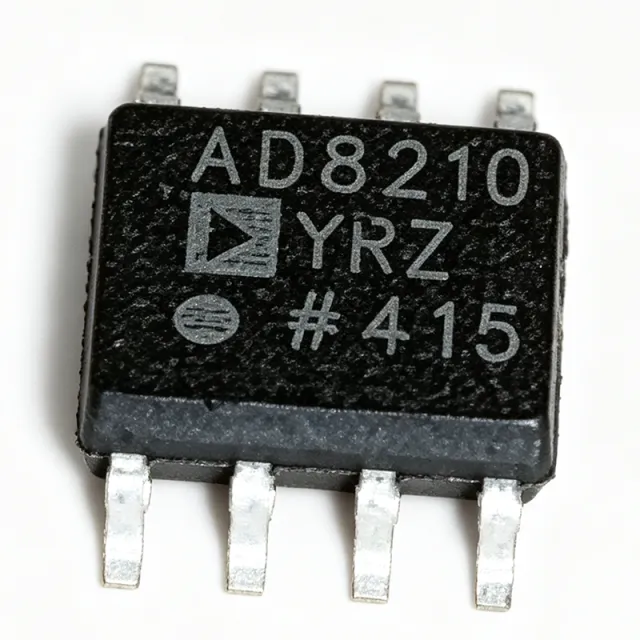
AD8210YRZ - High Voltage Bidirectional Current Shunt Monitor | Analog Devices
The AD8210YRZ is a high voltage, bidirectional current shunt monitor from Analog Devices, designed to amplify small differential voltages in the presence of large common-mode voltages. It operates from a single 5 V supply and features an input common-mode voltage range from -2 V to +65 V, making it ideal for high-side and low-side current sensing in automotive, industrial, and power management applications. The device is available in an 8-pin SOIC package and provides a 5 mA output current capability. A current shunt monitor is a specialized difference amplifier that measures the voltage drop across a sense resistor to determine load current. It is a critical component in power management systems, enabling precise current monitoring for battery management, motor control, and load protection. The AD8210 belongs to the family of current sense amplifiers, which are essential for closed-loop control and diagnostic functions in modern electronic systems. Key features of the AD8210YRZ include a wide common-mode input range, bidirectional current sensing capability, and excellent AC and DC performance. The device offers a typical supply current of 2 mA and a bandwidth of 450 kHz, ensuring accurate measurement of dynamic currents. Its high CMRR (typically 120 dB) rejects common-mode noise, making it suitable for noisy industrial environments. The AD8210 uses a precision difference amplifier architecture with an external shunt resistor, allowing flexible gain configuration. The output is referenced to a programmable level, enabling bidirectional current detection. The device includes an input filter to reduce high-frequency noise and supports both high-side and low-side sensing configurations. Typical applications include motor control, battery monitoring, power supply diagnostics, and load current sensing in automotive systems. The wide common-mode range and bidirectional capability make it particularly useful for H-bridge motor drivers and battery charge/discharge monitoring. When designing with the AD8210YRZ, ensure the shunt resistor is placed close to the load and the input filter components are optimized for the desired bandwidth. The output reference pins allow adjustment of the output voltage level, which is essential for interfacing with ADCs or comparators.
AD8212S - High Voltage Current Shunt Monitor | Analog Devices
The AD8212S is a high common-mode voltage, current shunt monitor from Analog Devices. It accurately amplifies a small differential input voltage in the presence of large common-mode voltages up to 65 V, and can operate at common-mode voltages greater than 500 V with the addition of an external PNP transistor. The device outputs a current proportional to the differential input voltage, making it ideal for current monitoring across a shunt resistor in applications controlling loads such as motors and solenoids. A current shunt monitor is a specialized amplifier that measures the voltage drop across a sense resistor placed in series with a load, converting this small differential voltage into a proportional output signal. In high-side sensing, the monitor must reject the large common-mode voltage present at the shunt, which can be tens or hundreds of volts above ground. The AD8212S excels in this role, providing accurate current measurement without requiring level shifting or isolation, simplifying the design of motor control, solenoid control, and power management systems. Key features of the AD8212S include a wide common-mode input range of 4.5 V to 65 V (extendable beyond 500 V with an external PNP), a current output that simplifies interfacing with ADCs or comparators, and a wide operating temperature range of -40°C to +125°C. The device operates from a single 5 V supply and draws a low quiescent current, making it suitable for automotive and industrial environments. Its high common-mode rejection ensures accurate current sensing even in noisy power systems. The AD8212S uses a precision bipolar process to achieve low offset and gain drift over temperature. The current output can be converted to a voltage with an external resistor, allowing flexible scaling. The device is available in a compact SOIC-8 package, which is pin-compatible with the standard AD8212, and is specified for operation over the extended temperature range, making it suitable for harsh environments. Typical applications include high-side current sensing in motor control, solenoid control, battery monitoring, and power supply monitoring. The device is also used in automotive systems for load detection and diagnostics. Its ability to handle high common-mode voltages with minimal external components makes it a preferred choice for robust current sensing. When designing with the AD8212S, ensure the supply voltage is within the specified range and the output resistor is chosen to keep the output voltage within the ADC's input range. The external PNP transistor, if used, must be selected to handle the required common-mode voltage and current.

AD8436ACPZ-R7 - 20MHz True RMS-to-DC Converter | Analog Devices
The Analog Devices AD8436ACPZ-R7 is a new-generation, translinear precision, low-power true RMS-to-DC converter that delivers a precise DC equivalent of the RMS value of complex AC waveforms, including switch-mode power supply and triac-derived signals. It offers 0.25% (B-grade) or 0.5% of reading accuracy across a wide dynamic input range of 3 mV RMS to 3 V RMS full-scale, with larger inputs supported via external attenuators. The device is housed in a 20-pin LFCSP (4 mm x 4 mm) package with an exposed pad. A true RMS-to-DC converter is an analog computing block that continuously extracts the root-mean-square energy of an arbitrary AC waveform and presents it as a stable DC voltage proportional to the signal's heating power. Unlike average-responding or peak-responding detectors, true RMS converters correctly measure signals with non-sinusoidal content such as PWM drive outputs, SCR phase-angle waveforms, and switching-converter ripple. The AD8436 belongs to the category hierarchy of RMS-to-DC converter -> AC measurement IC -> data acquisition -> signal chain -> power management specialized IC. Key features include a 20 MHz bandwidth, sub-100 microsecond settling at high input levels, an on-board output buffer amplifier, and an optional averaging capacitor that lets the user trade ripple versus settling time. The AD8436 also provides a peak-mode/average-mode option, allowing it to deliver average rectified value when required. Operating from a single supply of 4.5 V to 36 V (or dual +/-5 V to +/-18 V), and consuming only 365 microamps of quiescent current, the part is engineered for battery-powered and industrial-grade instrumentation. Technically, the AD8436 uses a proprietary translinear gain cell and matched monolithic transistor array to compute the implicit square, mean, and square-root functions in a single chip, eliminating the need for an external log-antilog circuit. The on-chip buffer allows direct drive of low-impedance loads, 1 mA or higher, while preserving DC accuracy. Typical applications include power-line monitoring, switch-mode power supply output sensing, industrial process-control instrumentation, audio amplitude metering, RF transmitter envelope detection, and precision multimeter AC sections. The wide supply range supports 24V industrial bus rails and 48V telecom input monitoring without external regulators. Designers should note that the on-chip averaging capacitor pin must be paired with the correct external capacitor value to control ripple and settling time. The exposed pad on the LFCSP package must be soldered to a copper pour for thermal dissipation and to achieve the stated bandwidth. This page consolidates distributor pricing, true drop-in alternatives, and design notes that go beyond the manufacturer datasheet to support faster component selection.

ADBMS6948 - 16-Channel Battery Monitor | Analog Devices
The ADBMS6948 is a 16-channel battery pack monitoring system from Analog Devices, designed for measuring up to 16 series-connected battery cells with exceptional accuracy. It features the industry's first parallel measurement architecture, enabling simultaneous cell voltage and pack current measurements. The device achieves a total measurement error (TME) of less than 3 mV over the full temperature range and lifetime, making it suitable for demanding automotive and energy storage applications. The ADBMS6948 operates over a measurement range of -2.5V to 5.5V, supporting various battery chemistries including NMC and LFP. It is available in a 64-lead LFCSP-SS (9x9 mm) package. A battery pack monitoring system is an integrated circuit that measures the voltage, current, and temperature of individual cells in a battery pack to ensure safe and efficient operation. It is a critical component in battery management systems (BMS), which are used in electric vehicles, energy storage systems, and backup power supplies. The ADBMS6948 belongs to the category of battery monitoring ICs, which are part of the broader power management integrated circuit (PMIC) family. These devices provide essential data for state-of-charge (SoC) and state-of-health (SoH) estimation, cell balancing, and protection against overvoltage, undervoltage, and overcurrent conditions. Key features of the ADBMS6948 include synchronous pack current and cell voltage measurements, short/over current detection with less than 2 μs response time, programmable detection time and threshold, dedicated outputs for MOSFET/contactor control, redundant measurement, algorithm, and fault pin, 10 general-purpose I/O (GPIO) channels, cell and board temperature measurements, and pack, load, and system diagnostic measurements. The device also includes an SPI interface with a maximum operating frequency of [DATA_NEEDED: SPI max frequency] MHz, enabling high-speed communication with a host microcontroller. The ADBMS6948's parallel measurement architecture is a significant advancement over traditional sequential measurement systems, as it allows simultaneous sampling of all cell voltages and pack current, improving the accuracy of power and energy calculations. This is particularly important in applications where load transients can cause voltage fluctuations, as the synchronous measurement ensures that the voltage and current readings are time-aligned. The device also features a dedicated FAULTB pin that generates an interrupt when any preprogrammed over or under thresholds on cell voltage, cell temperature, or delta measurements are violated, providing immediate fault notification to the system controller. Typical applications for the ADBMS6948 include mild hybrid electric vehicles, two-wheeler and three-wheeler electric vehicles, four-wheeler electric vehicle auxiliary batteries, backup battery systems, and energy storage systems (ESS). Its high accuracy and robust feature set make it ideal for automotive battery management, where safety and reliability are paramount. The device's ability to measure both cell voltages and pack current synchronously enables precise state-of-charge estimation, which is essential for maximizing battery life and performance. When designing with the ADBMS6948, it is important to consider the PCB layout to minimize noise and ensure accurate measurements. The device requires careful decoupling of the power supply and proper grounding to achieve the specified TME. Additionally, the SPI interface should be isolated if the battery pack is at a high potential relative to the host controller, using components such as the ADuM1441ARWZ digital isolator. The ADBMS6948 is recommended for new designs, indicating that it is a current product with ongoing support from Analog Devices.

ADE9153A - Single-Phase Energy Metering IC, mSure Autocalibration | Analog Devices
The Analog Devices ADE9153A is a highly accurate single-phase energy metering IC with built-in mSure autocalibration, packaged in a 32-lead LFCSP (5x5 mm) and targeting shunt-based residential and industrial metering applications. The device integrates three high-performance 24-bit sigma-delta ADCs delivering 88 dB signal-to-noise ratio (SNR) for accurate line voltage and current sensing across a wide dynamic range. It is recommended for new designs and replaces the earlier ADE7953 as the flagship single-phase metering platform in the ADI energy family. An energy metering IC (also called a metrology AFE) is a specialized mixed-signal SoC that combines analog front-end ADCs, a digital signal processor, and metrology firmware to compute active, reactive, and apparent energy in real time. The ADE9153A sits at the metering tier of the smart-grid hierarchy (AFE -> metering SoC -> smart meter -> AMI), enabling tamper detection, power-quality monitoring, and RMS calculations on a single chip. Compared with discrete ADC+MCU designs, the integrated metrology engine reduces BOM, calibration effort, and time-to-market for Class 0.5/1.0 single-phase meters. Key features include built-in mSure autocalibration that removes the need for an accurate reference source or reference meter, support for shunt-resistor current sensing (no CT required), and an advanced measurement set covering active energy, fundamental reactive energy, apparent energy, line voltage and current RMS, and power-quality metrics. Communication is via SPI and I2C interfaces to an external host MCU, and the device operates over the industrial -40 °C to +85 °C temperature range. The 1ku list price starts from $4.38 per unit. Typical applications include single-phase smart meters, energy monitoring plugs and PDUs, solar PV string monitors, EV charging station metering, and home energy displays. The mSure autocalibration routine is especially valuable in high-volume manufacturing where reference instrumentation is the production bottleneck. When designing with the ADE9153A, observe the reference manual's PCB layout guidelines: place the shunt sensor in close proximity to the LINE/NEUTRAL sense inputs, provide a solid analog/digital ground split, and route the SPI/I2C signals away from the switched-mode power stage. Always validate calibration with the official ADE9153A evaluation kit (EV-ADE9153ASHIELDZ) before locking down firmware calibration constants. This page synthesizes distributor pricing, verified same-brand and cross-brand drop-in alternatives, and practical design notes from the ADE9153A technical reference manual - information not consolidated on any single manufacturer or distributor page.