STM32F767NIH6 vs STM32F767BIT6 Comparación
Comparación detallada lado a lado de STM32F767NIH6 por STMicroelectronics y STM32F767BIT6 por STMicroelectronics. Compare las especificaciones clave, los parámetros eléctricos, el encapsulado, el estado del ciclo de vida, los precios y la disponibilidad para determinar el mejor componente para los requisitos de su diseño.
STMicroelectronics
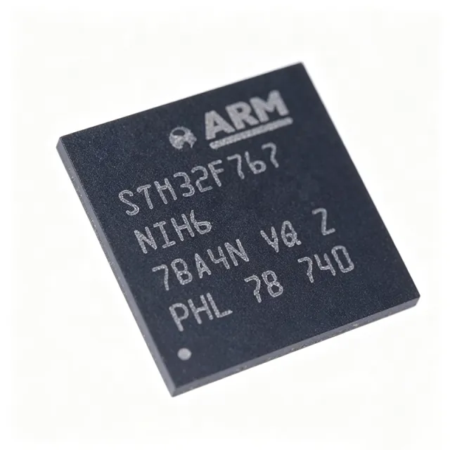
STM32F767NIH6 - 32-bit ARM Cortex-M7 MCU, 2MB Flash, 216MHz | STMicroelectronics
STM32F767NIH6 ✓ ActivoSTMicroelectronics

STM32F767BIT6 - ARM Cortex-M7 MCU, 2MB Flash, 216MHz | STMicroelectronics
STM32F767BIT6 ✓ ActivoComparación de especificaciones
| Parámetro | STM32F767NIH6 | STM32F767BIT6 |
|---|---|---|
| Marca | STMicroelectronics | STMicroelectronics |
| Categoría | Microcontrollers | Microcontrollers |
| Estado del ciclo de vida | Activo | Activo |
| Estado del stock | In Stock | In Stock |
| Precio unitario (USD) | $10,85 | $11,85 |
| Core | Arm 32-bit Cortex-M7 with double-precision FPU | ARM Cortex-M7 with FPU + DSP instructions |
| Frecuencia de reloj máxima | 216 MHz | — |
| CoreMark / DMIPS | 462 DMIPS / 2.14 DMIPS/MHz (Dhrystone 2.1) | — |
| Cache | 16 Kbytes I/D L1-cache | — |
| Program Memory Size | 2 MB Flash (dual-bank) | — |
| RAM Memory Size | 512 KB SRAM | — |
| Operating Voltage Range | 1.7 V to 3.6 V | — |
| Rango de temperatura de funcionamiento | -40 C to +85 C (industrial grade) | — |
| Number of I/O Lines | 159 | — |
| External Data Bus | 32-bit | — |
| External Address Bus | 26-bit | — |
| Encapsulado | TFBGA-216 (13x13mm, 0.8mm pitch) | 208-LQFP (28x28 mm), 0.5 mm pitch |
| I2C Interfaces | 4 | — |
| UART / USART | 4 USART + 4 UART | — |
| SPI Interfaces | 6 | — |
| CAN Interfaces | 3 | — |
| USB Interfaces | 2x USB OTG | — |
| Ethernet | 1x 10/100 MAC | — |
| SDMMC | 1x | — |
| ADC | 16-bit, up to 3.6 MSPS | 3 x 12-bit, up to 2.4 MSPS each |
| DAC | 12-bit | 2 x 12-bit |
| Cryptography | AES, DES, 3DES, TRNG | — |
| Graphics | Chrom-ART Accelerator, TFT LCD controller, JPEG codec | — |
| DSP | Yes (DSP instructions) | — |
| Estado RoHS | Compliant | Compliant |
| Maximum CPU Clock | — | 216 MHz |
| DMIPS | — | 462 DMIPS (2.14 DMIPS/MHz, Dhrystone 2.1) |
| Program Flash | — | 2 MB (single-bank, 32-bit fetch) |
| SRAM | — | 384 KB DTCM + 128 KB SRAM + 4 KB backup SRAM |
| L1 Cache | — | 16 KB I-cache + 16 KB D-cache |
| ART Accelerator | — | Yes (0-wait-state execution from Flash) |
| Operating Voltage | — | 1.7 V to 3.6 V |
| I/O Pins (max) | — | 162 GPIOs |
| Timers | — | up to 18 channels incl. 32-bit, IC/OC, PWM |
| USB | — | USB 2.0 OTG FS + HS with integrated HS PHY |
| CAN | — | 2 x CAN 2.0B |
| Crypto / Hash | — | AES-256, SHA-1/2, TRNG (hardware) |
| External Memory Bus | — | SDRAM (up to 32-bit) + SRAM/PSRAM/NOR/NAND |
| Display Controller | — | LCD-TFT, up to 1024x768 + DMA2D |
| Octo-SPI / Quad-SPI | — | 1 x Octo-SPI / 1 x Quad-SPI |
| Temperatura de funcionamiento | — | -40°C to +85°C (Grade 6) |
| Tipo de montaje | — | Surface Mount |
| Nivel MSL | — | 3 (per JEDEC J-STD-020) |