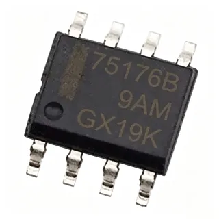
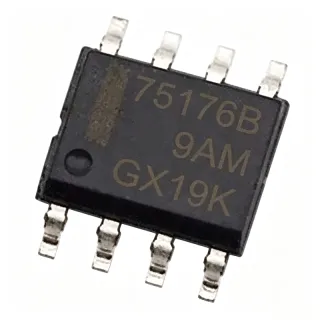
ESD5V0L3 - 5V 3-Line ESD Protection TVS Array | SOT-143
N.º de pieza: ESD5V0L3 ✓ Activo| Cant. | Precio unitario | Total |
|---|---|---|
| 1 | $0.18 | $0,18 |
| 10 | $0.15 | $1,50 |
| 100 | $0.12 | $12,00 |
| 500 | $0.09 | $45,00 |
| 1.000 | $0.07 | $70,00 |
| 3.000 | $0.05 | $150,00 |
ESD5V0L3 Descripción general
A TVS diode array is a specialized class of transient voltage suppressor that uses one or more avalanche-breakdown diodes to clamp voltage spikes within nanoseconds, much faster than the air-discharge or contact-discharge waveforms defined by IEC 61000-4-2. In the broader component taxonomy, the ESD5V0L3 belongs to the TVS/ESD protection family, which itself falls under discrete semiconductors and circuit protection, sitting alongside multilayer varistors (MLVs), polymer ESD suppressors, and gas discharge tubes.
Key features include a low clamping voltage on the order of ~12V at typical 8/20µs surge current, ultra-low leakage current in the nanoampere range at the 5V working voltage, sub-nanosecond response time to ESD transients, and a minimal junction capacitance suited for data lines up to several hundred Mbps. The SOT-143 footprint (approximately 2.9 mm x 1.3 mm body with 4 leads) keeps board area to a minimum, freeing routing space on dense mobile, wearable, and IoT PCBs.
The internal architecture is three unidirectional steering diodes plus a central Zener TVS clamp, sharing a common ground-return pin so that any of the three protected lines can dump energy safely to ground during a positive or negative ESD event. Because each channel is unidirectional, designers should orient the array so the protected IC pin sees the cathode side of the diode. Forbidding reverse polarity is important; if bidirectional protection is needed, look to parts explicitly marketed as bidirectional.
Typical applications include mobile phone data-line protection, USB 1.x downstream ports, headphone and microphone interfaces, SIM/MMC card sockets, industrial push-button and key-scan lines, and any 5V-tolerant GPIO/connector exposed to human-contact ESD. The unidirectional 5V rail level also suits 3.3V systems when the working-voltage margin is acceptable.
When designing with this part, keep the protected trace as short as possible and place the ESD5V0L3 within 10 mm of the external connector. Use a solid ground pour on the ground pin to keep the discharge loop inductance low; failure to do so will degrade clamping performance because the residual inductance of a thin ground trace adds directly to the residual voltage seen by the protected IC.
This page consolidates the manufacturer datasheet, distributor availability, and a drop-in alternative cross-reference set that is not available on a single competitor datasheet page, giving procurement and design engineers a one-stop reference for the ESD5V0L3.
Alternativas directas para ESD5V0L3 — mismo encapsulado, compatible pin a pin. Se excluyen las piezas de otro encapsulado que requieren retrabajo de la PCB.
Herramienta de comparación rápida — seleccione piezas alternativas para compararlas lado a lado:
ESD5V0L3-YINT
✅ Sustitución directa📋 Alternativa de referencia (no en el catálogo)
ESD5V0S3
✅ Sustitución directa📋 Alternativa de referencia (no en el catálogo)
ESD5V0L3 Especificaciones
| Manufacturer | Shanghai Yint Electronic Co., Ltd (YINT) |
| Part Description | Three-Lines ESD Protection TVS Array |
| Working Voltage (Vrwm) | 5.0 V |
| Polarity | Unidirectional |
| Number of Protected Lines | 3 |
| Encapsulado | SOT-143 |
| Tipo de montaje | Surface Mount |
| Temperatura de funcionamiento | -55C to +150C (typical TVS diode range) |
| Lead Finish | Matte Tin (Pb-free) |
| Estado RoHS | Compliant |
Configuración de pines de ESD5V0L3
| Pin 1 | CH1 / I/O 1 — Channel 1 - protected I/O line 1 (per YINT datasheet pinout) |
| Pin 2 | CH2 / I/O 2 — Channel 2 - protected I/O line 2 (per YINT datasheet pinout) |
| Pin 3 | GND — Common ground return for all three channels; bond to chassis/earth ground with low impedance |
| Pin 4 | CH3 / I/O 3 (TAB) — Channel 3 - protected I/O line 3; shared with the heat-dissipation tab (per YINT datasheet pinout) |
Aplicaciones típicas
ESD5V0L3 es adecuado para 7 aplicacións: Mobile Phone Audio Jack Protection, USB 1.x Downstream Port Protection, SIM / MMC Card Socket Protection, Industrial Key-Scan / Push-Button Lines, RS-232 / RS-485 Data Line Protection, IoT Sensor Node Connector Protection, 5V GPIO / Button Input Protection on Microcontroller Boards.
Mobile Phone Audio Jack Protection
The ESD5V0L3 protects left-channel, right-channel, and microphone-detect pins of 3.5 mm audio jacks from human-body ESD strikes during headphone insertion. With 5V working voltage it sits transparently in circuit until a transient occurs, then clamps the offending voltage on any of the three lines within nanoseconds to the common ground. Its SOT-143 footprint keeps board area minimal near the receptacle, freeing space for the audio codec and Class-D amplifier. Pair with a low-impedance ground pour on Pin 3 to keep clamp voltage low during real-world IEC 61000-4-2 contact-discharge events.
Recomendado
USB 1.x Downstream Port Protection
The ESD5V0L3 protects D+, D-, and VBUS-sense lines of a USB 1.x (Low or Full Speed) downstream port against cable-discharge and hot-plug ESD events. The 5V working voltage matches the VBUS rail, and its typical junction capacitance is low enough to preserve the 1.5 Mbps or 12 Mbps USB signal integrity without measurable eye-diagram degradation. Place the array within 10 mm of the USB receptacle with Pin 3 bonded directly to the chassis-ground shield for minimum loop inductance. For USB 2.0 High Speed or USB 3.0 SuperSpeed, instead use an array with capacitance below 0.5 pF typ.
Recomendado
SIM / MMC Card Socket Protection
The ESD5V0L3 protects the CLK, DATA, and RESET (or CMD) lines of a SIM card or MMC card socket against user-contact ESD when the user inserts or removes the card. The 5V working voltage matches the SIM VCC rail in legacy designs, and the unidirectional topology correctly orients the diode cathode to the protected IC side. Its SOT-143 package saves space next to the card connector where board real estate is at a premium. This preserves the integrity of authentication handshakes that would otherwise be corrupted by an ESD event during card insertion.
Recomendado
Industrial Key-Scan / Push-Button Lines
The ESD5V0L3 protects three adjacent key-scan rows or columns of a matrix keypad, push-button arrays, or rotary-encoder inputs commonly found on industrial HMI panels. The 5V working voltage tolerates the typical 3.3V or 5V CMOS logic swing, and its sub-nanosecond response catches contact-discharge events before they reach the scanning MCU. Place one array per group of three key lines; for larger matrices, use multiple arrays sharing a common ground plane. The SOT-143 footprint fits cleanly between the connector and the MCU, keeping signal-trace lengths short.
Recomendado
RS-232 / RS-485 Data Line Protection
The ESD5V0L3 protects TX, RX, and a third control line (such as RTS or direction-control) on an RS-232 or RS-485 transceiver exposed to cable-discharge events when field wiring is connected or disconnected. Its 5V working voltage suits legacy 5V transceivers, while the low junction capacitance is acceptable for low-speed RS-232 (up to 115.2 kbps) and most RS-485 (up to 10 Mbps) data rates. Bond the common ground pin to chassis ground at the transceiver end to shunt transient currents away from the bus pins. For higher bus voltages, select an array rated for the appropriate working voltage.
Recomendado
IoT Sensor Node Connector Protection
The ESD5V0L3 protects the three external I/O pins (such as UART TX/RX/reset or SPI CS/MOSI/MISO) of a battery-powered IoT sensor node exposed to user-touch ESD. Its nanoampere leakage at the 5V working voltage is negligible against the node's overall quiescent budget, and the SOT-143 package supports tight spacing in miniature wearable or smart-sensor form factors. Place near the external connector with a low-impedance ground return so the array can keep residual voltage below the protected IC's absolute-maximum rating during contact discharge.
Recomendado
5V GPIO / Button Input Protection on Microcontroller Boards
The ESD5V0L3 protects three 5V-tolerant GPIO pins of a microcontroller board against human-contact ESD when the board is handled, plugged into a chassis, or interfaced with external wiring. It clamps transient energy on each pin to ground while remaining invisible to legitimate 3.3V or 5V logic signalling during normal operation. Placing one array per group of three GPIOs lets you shield the MCU from ESD without compromising the GPIO's high-speed switching capability. This pattern is especially valuable in evaluation kits and developer boards shipped to end users.
Recomendado
Resumen de productos recomendados
Datos de referencia de ingeniería para ESD5V0L3 — comparación, orientación de diseño e información de cumplimiento.
Guía de selección
Comparación con alternativas
| Parámetro | Este producto | ESD5V0L3-YINT | ESD5V0S3 |
|---|---|---|---|
| Brand | YINT | YINT (same part alias) | YINT (same family) |
| Package | SOT-143 | SOT-143 (same) | SOT-143 (same) |
| Working Voltage (Vrwm) | 5.0 V | 5.0 V | 5.0 V |
| Number of Protected Lines | 3 | 3 | 3 |
| Polarity | Unidirectional | Unidirectional | Unidirectional |
| Mounting Type | Surface Mount | Surface Mount | Surface Mount |
| Channel-to-Pin Map | 1=CH1, 2=CH2, 3=GND, 4=CH3 | 1=CH1, 2=CH2, 3=GND, 4=CH3 (identical) | 1=CH1, 2=CH2, 3=GND, 4=CH3 (same family) |
| RoHS Status | Compliant | Compliant | Compliant |
| Packaging | Tape & Reel, 3000 pcs | Tape & Reel, 3000 pcs | Tape & Reel, 3000 pcs |
Diferenciadores clave
- Three-line 5V unidirectional protection in SOT-143 (frente a Single-line TVS diode (e.g. PESD5V0L1BA))
- Industry-standard SOT-143 footprint (frente a BGA-array TVS for high-channel count (e.g. 4-channel or 6-channel BGA))
- 5V working voltage matched to legacy 5V logic rails (frente a 3.3V-only TVS array (e.g. 3.3V Vrwm parts))
Notas de diseño
Place the ESD5V0L3 within 10 mm of the external connector so the protected trace length is minimized. Bond Pin 3 (ground) to a low-impedance chassis/earth ground pour - preferably a filled ground plane on the top or inner layer - to keep the ground-loop inductance under a few nH. Long ground traces will degrade clamping performance during a real IEC 61000-4-2 discharge because the residual inductance adds directly to the residual voltage seen by the protected IC.
Route the protected lines directly through the device without stubs, vias, or sharp bends. Avoid routing any other signal above or below the protected trace on adjacent layers to minimize coupling into the discharge loop. The SOT-143 tab (Pin 4) should be soldered to a copper pad connected to Pin 3 ground for both thermal dissipation and lowest ground impedance, rather than left floating or connected to a signal trace.
Estimated: The ESD5V0L3 is unidirectional - orient it so the cathode side faces the protected IC pin. If oriented backwards, the protected IC will forward-bias the steering diode during normal signal swing, potentially clamping legitimate signal transitions and causing logic-level errors or even damage. For bidirectional signal applications, choose a part explicitly marketed as bidirectional (such as those with 'C' or 'B' in the suffix) rather than trying to mirror two unidirectional arrays.
Do not rely on the ESD5V0L3 alone for EFT (electrical fast transient) or surge (lightning) protection - it is optimized for ESD and cable-discharge events. For IEC 61000-4-4 EFT or IEC 61000-4-5 surge immunity, add a bulk TVS or PTC fuse upstream of the ESD array. The YINT datasheet should be reviewed for the specific 8/20µs peak-pulse-current rating before relying on the part for surge events beyond its rated pulse current.
Información de cumplimiento
RoHS compliance and lead-free matte-tin finish confirmed by YINT product page. REACH, halogen-free, and conflict-mineral declarations not explicitly published in the verified web data - set to unknown. AEC-Q100 not applicable because this is a discrete TVS array, not an automotive-qualified IC.