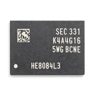
H5TQ4G63EFR-RDC - 4Gb DDR3 SDRAM, 1.5V FBGA-96 | SK hynix
N.º de pieza: H5TQ4G63EFR-RDC ✓ Activo| Cant. | Precio unitario | Total |
|---|---|---|
| 1 | $17.15 | $17,15 |
| 10 | $15.85 | $158,50 |
| 100 | $14.6 | $1.460,00 |
| 500 | $13.4 | $6.700,00 |
| 1.000 | $12.3 | $12.300,00 |
H5TQ4G63EFR-RDC Descripción general
DDR3 SDRAM (Double Data Rate 3 Synchronous Dynamic Random Access Memory) is a JEDEC-defined volatile memory technology that transfers data on both edges of the clock, achieving high bandwidth at low operating voltage compared to its DDR2 predecessor. Within the memory hierarchy, it sits as the main-system-memory class of DRAM, below CPU caches and above storage, and is a core building block of any embedded power-management and computing design.
Key features of the H5TQ4G63 family include automatic self-refresh, auto precharge function, an asynchronous reset function for reliable initialization, a data mask (DM) function, dynamic on-chip termination (ODT), ZQ calibration for output driver accuracy, and write leveling for fly-by topology support. These features enable robust high-speed operation on multi-rank PCB designs.
The device uses CMOS bank architecture with standard DDR3 command interface (CK/CK# differential clocking) and supports the JEDEC DDR3 feature set as documented in the manufacturer datasheet. The EFR generation offers improved speed grades and reduced refresh current versus the earlier AFR generation (for example H5TQ4G63AFR-G7C), extending battery-powered and thermally constrained designs.
Typical applications include embedded industrial controllers, networking equipment, set-top boxes, test and measurement instrumentation, and FPGA-based processing systems that require 4Gb of dense main memory on a compact footprint.
When designing with this device, verify the speed grade suffix (RDC vs TEC vs H9C), match the controller's DDR3 timing parameters, and plan ZQ calibration and termination resistor placement carefully per the datasheet layout guidance.
This page synthesizes distributor pricing, family drop-in alternatives, and practical design notes not found in a single manufacturer datasheet.
Alternativas directas para H5TQ4G63EFR-RDC — mismo encapsulado, compatible pin a pin. Se excluyen las piezas de otro encapsulado que requieren retrabajo de la PCB.
Variantes de esta serie
Modelos de la misma serie compatibles directamente con H5TQ4G63EFR-RDC (mismo factor de forma y huella) — difiere en Organization, Package.
Herramienta de comparación rápida — seleccione piezas alternativas para compararlas lado a lado:
H5TQ4G63EFR-TEC
✅ Sustitución directa📋 Alternativa de referencia (no en el catálogo)
H5TQ4G63MFR-H9C
✅ Sustitución directa📋 Alternativa de referencia (no en el catálogo)
H5TQ4G63AFR-G7C
✅ Sustitución directa📋 Alternativa de referencia (no en el catálogo)
H5TQ4G63AFR-H9C
✅ Sustitución directa✓ En stock
$6.5 / unidad
Ver hoja de datos →H5TQ4G63AFR-PBC
✅ Sustitución directa📋 Alternativa de referencia (no en el catálogo)
H5TQ4G63EFR-RDC Valores máximos y características eléctricas
| Tipo de memoria | DDR3 SDRAM |
| Tamaño de memoria | 4 Gbit |
| Organización de memoria | 512M x 8 |
| Supply Voltage (VDD) | 1.425 V to 1.575 V (1.5 V typ.) |
| Clock Rate | 1.066 GHz class |
| Encapsulado | FBGA-96 |
| Temperatura de funcionamiento | 0C to +95C (RDC grade) |
| Tipo de montaje | Surface Mount |
| Interfaz | DDR3 (parallel, JEDEC DDR3 command interface) |
| Data Mask | Yes (DM function) |
| On-Chip Termination | Dynamic ODT |
| ZQ Calibration | Yes |
| Write Leveling | Yes |
| Asynchronous Reset | Yes |
| Auto Self-Refresh | Yes |
| Auto Precharge | Yes |
| Estado RoHS | Compliant |
| Manufacturer | SK hynix (Hynix Semiconductor) |
Guía de configuración de pines de H5TQ4G63EFR-RDC fbga-96
Configuración de pines para H5TQ4G63EFR-RDC (encapsulado fbga-96). Este CI digital incluye GPIO, interfaces de comunicación (UART, SPI, I2C) y pines de alimentación. Consulte la hoja de datos del fabricante para conocer las funciones alternativas de los pines y las opciones de configuración. Esencial para el diseño de sistemas embebidos y el diseño de PCB.

No hay datos detallados de patillaje disponibles para H5TQ4G63EFR-RDC.
Consulte la hoja de datos para ver la configuración completa de patillas.
Aplicaciones típicas
H5TQ4G63EFR-RDC es adecuado para 6 aplicacións: Embedded Industrial Controllers, Networking and Communication Equipment, FPGA-Based Processing and Image Processing, Test and Measurement Instrumentation, Set-Top Box and Smart Home Hubs, Power Sequencing and Memory Subsystem Bring-Up.
Embedded Industrial Controllers
Industrial PLCs, motion controllers and HMI platforms rely on the H5TQ4G63 as dense main memory where 4Gb in a single 96-ball FBGA keeps PCB area small inside cramped DIN-rail enclosures. The 1.5V SSTL15 interface reduces I/O power versus DDR2, and the dynamic ODT plus ZQ calibration features hold signal integrity across the factory temperature swings that would otherwise require re-termination. For environments below 0C, the EFR-TEC industrial grade (-40C to +95C) should be specified instead of the RDC commercial grade, since commercial-grade self-refresh timing is not characterized at deep sub-zero temperatures and cold-start failures are difficult to diagnose in the field.
Recomendado
Networking and Communication Equipment
Enterprise switches, routers and base-station line cards use the H5TQ4G63 as packet-buffer memory, where its 1066 Mbps-class bandwidth absorbs burst traffic between MACs and CPUs. Write leveling specifically matters here: fly-by clock routing across multiple ranks is standard on network boards, and the H5TQ4G63's leveling support lets controllers deskew DQS per byte lane without per-rank clock stubs. Data mask support allows byte-granular write masking when updating packet headers in place, cutting effective write latency. Multi-rank designs combining several H5TQ4G63 devices should budget refresh and termination current into the power supply design, since dynamic ODT draws significant instantaneous current during bus turnarounds.
Recomendado
FPGA-Based Processing and Image Processing
Xilinx 7-series and similar FPGA systems use the H5TQ4G63 as frame-buffer and coefficient storage for video pipelines and machine-vision engines. A single 4Gb x8 device stores multiple full-HD frames, and the DDR3 interface's auto precharge reduces controller overhead during the linear-burst access patterns typical of frame streaming. Because image pipelines are latency-sensitive, designers should place the FPGA and SDRAM with matched-length, fly-by-free routing when using a single rank, and implement read-gating calibration in the MIG controller. The asynchronous reset function guarantees deterministic initialization of the SDRAM after power glitches, an important recovery path in unattended camera installations.
Recomendado
Test and Measurement Instrumentation
Oscilloscopes, logic analyzers and signal generators require deep capture memory with sustained write bandwidth; the H5TQ4G63's 4Gb capacity and 1066 Mbps-class interface let instruments buffer seconds of acquisition data on a compact two-rank PCB footprint. The ZQ calibration function maintains driver impedance accuracy as the instrument heats up during long acquisitions, protecting the DDR3 eye margin, while dynamic ODT simplifies multi-load bus design on shared capture buses. Instrument designers should derate operating frequency if the ambient inside the chassis exceeds +85C, since the RDC grade tops out at +95C junction and self-heating at full bandwidth is significant. EFR generation dies offer lower refresh current, extending margin in fanless designs.
Recomendado
Set-Top Box and Smart Home Hubs
IPTV set-top boxes and smart-home hubs use the H5TQ4G63 as main memory for an application SoC running video decode stacks. Its 4Gb capacity comfortably hosts a Linux software stack plus multiple HD video buffers, and the low 1.5V core power helps products meet energy-star standby targets by allowing shallow power-down states between decode bursts. The auto self-refresh feature lets the SoC clock-gate the memory controller during idle periods while retaining application state, cutting quiescent power dramatically. Consumer products typically use the commercial RDC temperature grade, but wall-mounted hubs in sun-exposed locations should verify enclosure temperatures stay below +95C or move to the TEC grade.
Recomendado
Power Sequencing and Memory Subsystem Bring-Up
DDR3 subsystems need a reliable power tree: VDD/VDDQ rails within 1.425V-1.575V and correct ramp sequencing before the asynchronous reset is released. The H5TQ4G63's asynchronous reset input provides a hardware-safe initialization point, and supervisory ICs can drive it directly to guarantee the memory enters a known state after brownouts - a common field-failure mode in embedded systems. During board bring-up, designers should verify ZQ calibration completes before first access, confirm write-leveling results per byte lane, and check termination current during bus turnarounds on the scope. Correct supply design here eliminates the majority of intermittent DDR3 issues reported in production.
Recomendado
Resumen de productos recomendados
Datos de referencia de ingeniería para H5TQ4G63EFR-RDC — comparación, orientación de diseño e información de cumplimiento.
Guía de selección
Comparación con alternativas
| Parámetro | Este producto | H5TQ4G63EFR-TEC | H5TQ4G63MFR-H9C | H5TQ4G63AFR-G7C | H5TQ4G63AFR-PBC |
|---|---|---|---|---|---|
| Package | FBGA-96 | FBGA-96 - same | FBGA-96 - same | FBGA-96 - same | FBGA-96 - same |
| Brand | SK hynix | SK hynix | SK hynix | SK hynix (Hynix Semiconductor) | SK hynix (Hynix Semiconductor) |
| Memory Size | 4 Gbit | 4 Gbit | 4 Gbit | 4 Gbit | 4 Gbit |
| Organization | x8 (512M x 8) | x8 | x8 | x8 | x8 |
| Supply Voltage | 1.425 V to 1.575 V | 1.425 V to 1.575 V | 1.425 V to 1.575 V | 1.425 V to 1.575 V | 1.425 V to 1.575 V |
| Die Generation | EFR | EFR | MFR | AFR (2012 release) | AFR (Aug 2012 initial release) |
| Feature Set (ODT / ZQ / Write Leveling) | Yes / Yes / Yes | Yes / Yes / Yes | Yes / Yes / Yes | Yes / Yes / Yes | Yes / Yes / Yes |
Diferenciadores clave
- Industrial temperature option in same footprint (frente a H5TQ4G63EFR-RDC)
- Newer EFR die generation with improved refresh characteristics (frente a H5TQ4G63AFR-G7C)
- Full DDR3 feature set for high-speed signal integrity (frente a H5TQ4G63AFR-PBC)
Notas de diseño
Design the DDR3 VDD/VDDQ rail for 1.5V +/- 5% (1.425V-1.575V) with adequate transient headroom: DDR3 termination current during bus turnarounds appears as fast load steps. Use a dedicated 1.5V regulator (or VTT termination rail per your controller reference design) and place bulk capacitance near the FBGA ball field. Verify the rail stays within tolerance including ZQ calibration transients; brownouts below 1.425V during operation corrupt DRAM state and require the asynchronous reset pin to be asserted for a clean recovery.
Follow JEDEC-style SSTL15 routing practice: length-match DQ to DQS within the controller's specified skew window, route CK/CK# as a tightly coupled differential pair, and reference all DDR3 signals to a solid ground plane. Place the 240-ohm 1% ZQ resistor close to the ZQ ball with a direct ground return - routing it near switching signals degrades calibration accuracy. For single-rank layouts, moderate fly-by routing still benefits from enabling write leveling in the controller to absorb residual CK-to-DQS skew.
The most common bring-up failures with the H5TQ4G63 are suffix mismatches and temperature mis-rating. Do not assume an RDC grade works at -20C: it is specified 0C to +95C only, and self-refresh timing is not characterized below 0C - specify the EFR-TEC grade for industrial ranges. Also verify your memory controller QVL for the specific die generation (EFR vs AFR), since refresh and timing parameters differ between generations, and re-run write-leveling/read-gate calibration whenever the die revision changes.
At the 1066 Mbps class, enable dynamic ODT and simulate the read/write eye with IBIS models from the manufacturer datasheet package before committing the stackup. Terminate DQ/DQS to VTT through the on-die ODT rather than external resistors where possible, and keep stub length from the main bus under a few hundred mils. If operating a multi-rank bus, enable write leveling and per-rank ODT settings per the controller reference manual to keep setup/hold margins positive across process corners.
Información de cumplimiento
RoHS compliance stated on JLCPCB listing for H5TQ4G63EFR-RDC. REACH, lead-free and halogen-free status not stated in provided data - confirm with SK hynix product page.