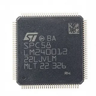
SPC5744PK1AMLQ5 - Dual e200Z4 150MHz Automotive MCU | NXP
N.º de pieza: SPC5744PK1AMLQ5 ✓ Activo| Cant. | Precio unitario | Total |
|---|---|---|
| 1 | $0 | $0,00 |
| 10 | $0 | $0,00 |
| 100 | $0 | $0,00 |
| 500 | $0 | $0,00 |
| 1.000 | $0 | $0,00 |
SPC5744PK1AMLQ5 Descripción general
A microcontroller (MCU) is a single integrated circuit that combines a processor core, memory, and peripherals into one chip, forming the computational heart of an embedded system. Within the power-management hierarchy of vehicle electronics, the MCU sits above sensor and actuator ICs and below domain controllers. The SPC5744PK1AMLQ5 belongs to NXP's MPC574xP family, built on the 32-bit embedded Power Architecture (e200 core family, originally developed with Freescale Semiconductor), which is widely deployed in automotive and industrial functional-safety systems.
Key differentiating features include the dual e200Z4 cores operating in lockstep (LS) mode for redundant execution, a Flash memory density of 2.5MB and 384kB of on-chip SRAM, and a 150 MHz core clock that balances real-time performance with power efficiency. The device is engineered to meet the highest functional-safety standards for automotive and industrial safety applications, and it integrates dedicated safety mechanisms on-chip.
From an architecture standpoint, the lockstep configuration executes the same instruction stream on both cores and compares results, detecting faults in real time - a technique central to ISO 26262-style functional-safety design. The Power Architecture instruction set provides deterministic interrupt latency and strong compiler toolchain support, including NXP's S32 Design Studio IDE.
Typical applications include automotive body and gateway control modules, electric powertrain and hybrid-vehicle control units, industrial motor control, and functional-safety-oriented automation controllers. The -40C to +125C ambient rating makes the part suitable for under-hood and harsh-environment deployments.
A key design consideration is thermal management: at full 150 MHz operation in an LQFP-144 surface-mount package, designers should budget junction temperature headroom against the +125C ambient rating and verify copper-pour thermal resistance on the PCB.
This page synthesizes distributor availability, family drop-in variants, packaging/MSL data, and practical sourcing guidance not consolidated in the manufacturer datasheet.
Alternativas directas para SPC5744PK1AMLQ5 — mismo encapsulado, compatible pin a pin. Se excluyen las piezas de otro encapsulado que requieren retrabajo de la PCB.
Herramienta de comparación rápida — seleccione piezas alternativas para compararlas lado a lado:
SPC5744PK1AMLQ8
✅ Sustitución directa📋 Alternativa de referencia (no en el catálogo)
SPC5744PK1AMLQ5R
✅ Sustitución directa📋 Alternativa de referencia (no en el catálogo)
SPC5744PFK1MLQ5
✅ Sustitución directa📋 Alternativa de referencia (no en el catálogo)
SPC5744PF1AMLQ5
✅ Sustitución directa📋 Alternativa de referencia (no en el catálogo)
SPC5741PK1AMLQ9
✅ Sustitución directa📋 Alternativa de referencia (no en el catálogo)
SPC5744PK1AMLQ5 Valores máximos y características eléctricas
| Core Architecture | 32-bit Power Architecture (e200) |
| Core Configuration | 2 x e200Z4 cores in lockstep (LS) |
| Frecuencia de reloj máxima | 150 MHz |
| Flash Memory | 2.5 MB |
| SRAM | 384 kB |
| Rango de temperatura de funcionamiento | -40C to +125C |
| Encapsulado | LQFP-144 |
| Tipo de montaje | Surface Mount |
| Ancho del bus de datos | 32 bit |
| Product Family | MPC574xP / SPC574xP |
| Functional Safety Target | Automotive and industrial functional safety applications |
| Nivel de sensibilidad a la humedad (MSL) | 3 |
| Peak Reflow Temperature | 260 C |
| Maximum Time at Peak Reflow | 40 s |
| Terminal Finish | Tin (JESD-609 code e3) |
Guía de configuración de pines de SPC5744PK1AMLQ5 lqfp-144
Configuración de pines para SPC5744PK1AMLQ5 (encapsulado lqfp-144). Este CI digital incluye GPIO, interfaces de comunicación (UART, SPI, I2C) y pines de alimentación. Consulte la hoja de datos del fabricante para conocer las funciones alternativas de los pines y las opciones de configuración. Esencial para el diseño de sistemas embebidos y el diseño de PCB.
No hay datos detallados de patillaje disponibles para SPC5744PK1AMLQ5.
Consulte la hoja de datos para ver la configuración completa de patillas.
Aplicaciones típicas
SPC5744PK1AMLQ5 es adecuado para 6 aplicacións: Automotive Body and Gateway Control, Electric Powertrain and Hybrid Control, Industrial Functional-Safety Automation, Chassis and Safety Domain Control, Industrial Motor Control, Telematics and Connectivity Gateways.
Automotive Body and Gateway Control
The SPC5744PK1AMLQ5 fits automotive body control modules and gateway ECUs because its dual lockstep e200Z4 cores at 150 MHz deliver the deterministic real-time behavior required for CAN/LIN/FlexRay message routing and diagnostics, while 2.5MB Flash accommodates protocol stacks, bootloader, and OTA update images with headroom. In a gateway role, the MCU runs the communication stack on the lockstep pair for fault detection, with 384kB SRAM buffering message queues. The -40C to +125C rating covers under-dash and engine-bay mounting locations without derating.
Recomendado
Electric Powertrain and Hybrid Control
In electric and hybrid powertrain control units, the SPC5744PK1AMLQ5 provides the functional-safety execution platform demanded by traction-inverter and battery-management control: the e200Z4 lockstep cores execute torque-control loops at 150 MHz with redundant computation for fault detection, and integrated safety mechanisms support the highest functional-safety targets cited by NXP for the MPC574xP family. The 2.5MB Flash stores motor models and calibration tables, while the +125C ambient rating suits the thermally stressed environment near inverters.
Recomendado
Industrial Functional-Safety Automation
For industrial automation controllers requiring functional-safety certification, the SPC5744PK1AMLQ5 offers automotive-grade robustness at industrial scale: the dual-core lockstep architecture detects computation faults in real time, and the Power Architecture instruction set provides the deterministic interrupt response needed for safety-rated motion and process control. With 2.5MB Flash for protocol and application code, 384kB SRAM for runtime data, and a -40C to +125C operating envelope, it serves safely rated PLC I/O, drives, and robotics controllers.
Recomendado
Chassis and Safety Domain Control
Chassis-domain ECUs such as steering-support and stability controllers benefit from the SPC5744PK1AMLQ5's lockstep e200Z4 pair, whose redundant execution and result comparison provide the fault-detection backbone that NXP states meets the highest functional-safety standards. The 150 MHz core clock services sensor-fusion algorithms and actuator control loops within strict timing windows, while the 2.5MB Flash holds safety monitor code and application logic. The LQFP-144 package supports the dense multi-rail PCB topologies typical of chassis modules.
Recomendado
Industrial Motor Control
The SPC5744PK1AMLQ5 is well suited to advanced industrial motor drives: the dual e200Z4 cores at 150 MHz execute field-oriented control algorithms with cycle-level determinism, the 384kB SRAM supports current-loop state data and observers, and on-chip timing peripherals generate PWM with fault shutdown. NXP positions the MPC574xP family explicitly for industrial functional-safety applications, making the device a fit for safely rated servo drives and traction drives where both performance and diagnostic coverage are required across the -40C to +125C range.
Recomendado
Telematics and Connectivity Gateways
Connected-vehicle telematics control units use the SPC5744PK1AMLQ5 as the real-time safety anchor behind the connectivity modem: it terminates vehicle bus traffic, executes diagnostics, and guards against unauthorized actuation, while its 2.5MB Flash holds multiple firmware slots for secure over-the-air updates. The lockstep cores provide the integrity monitoring that connectivity-exposed ECUs increasingly require, and the +125C rating plus MSL 3 assembly classification align with standard automotive manufacturing flows.
Recomendado
Resumen de productos recomendados
Datos de referencia de ingeniería para SPC5744PK1AMLQ5 — comparación, orientación de diseño e información de cumplimiento.
Guía de selección
Comparación con alternativas
| Parámetro | Este producto | SPC5744PK1AMLQ8 | SPC5744PFK1MLQ5 | SPC5741PK1AMLQ9 |
|---|---|---|---|---|
| Package | LQFP-144 | LQFP-144 - same | LQFP-144 - same | LQFP-144 - same |
| Brand | NXP Semiconductors | NXP Semiconductors | NXP Semiconductors | NXP Semiconductors |
| Core Configuration | 2 x e200Z4 in lockstep | 2 x e200Z4 in lockstep | 2 x e200 lockstep (verify grade) | 2 x e200 lockstep (verify grade) |
| Operating Temperature | -40C to +125C | -40C to +125C | -40C to +125C | -40C to +125C |
| Automotive Safety Targeting | Highest functional-safety standards (per NXP) | Same family safety architecture | Same family safety architecture | Same family safety architecture |
Diferenciadores clave
- Maximum memory density in the drop-in-compatible variant set (frente a SPC5741PK1AMLQ9)
- Dual-core lockstep safety architecture (frente a SPC5744PFK1MLQ5)
- 150 MHz performance at moderate power (frente a SPC5744PK1AMLQ8)
Notas de diseño
The -40C to +125C rating is an ambient specification. At sustained 150 MHz dual-core operation, budget junction temperature headroom by calculating internal dissipation from the MPC574xP power figures in the datasheet and verifying theta-JA against your PCB copper area. Estimated: for a typical LQFP-144 theta-JA of roughly 40-50 C/W (verify against NXP's thermal application note for your board stack-up), 1W of dissipation adds about 40-50C to junction temperature - leaving the sum below the absolute maximum junction limit is mandatory for reliability.
Follow NXP's MPC574xP hardware design guidelines: place decoupling capacitors on each supply rail pin pair, use solid ground planes under the LQFP-144, and keep the oscillator traces short and guarded. Program the device's built-in safety mechanisms (clock supervision, memory ECC) at boot rather than leaving them at reset defaults - this is central to realizing the functional-safety capability the family is designed for.
Respect the MSL 3 floor-life: once the moisture-barrier bag is opened, the parts must be reflowed within the MSL 3 window or baked per J-STD handling practice before soldering; peak reflow is 260C for a maximum of 40 seconds. Also, when substituting family variants (Q5/Q8/F/K grades), confirm the memory map and safe peripheral configuration against your software baseline - lockstep MCUs fail loudly but memory-size mismatches fail silently at link time.
Información de cumplimiento
Terminal finish is tin per JESD-609 code e3 (lead-free terminations), and MSL 3 / 260C / 40s reflow data per Partstack component records. Full RoHS/REACH/AEC-Q100 declarations must be obtained from NXP's environmental quality documentation on the official product page.