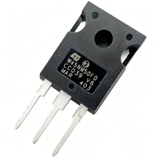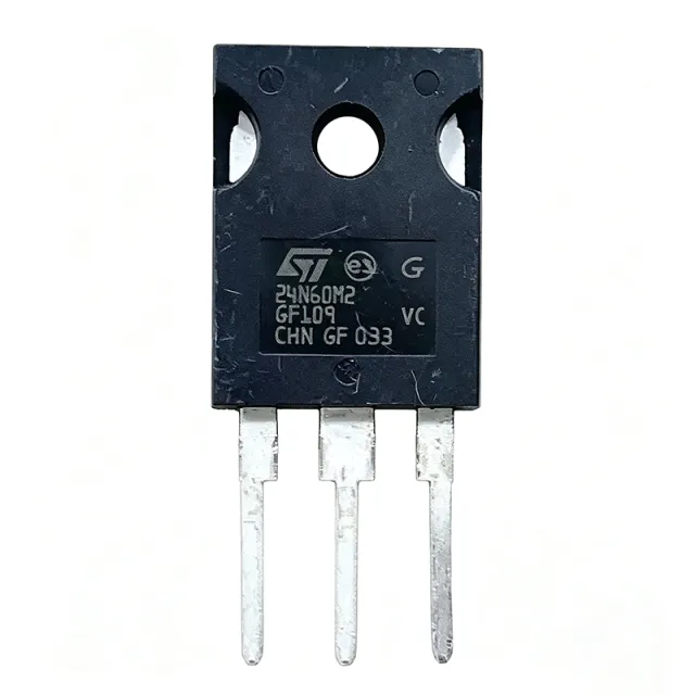
STW18N60M2 - 650V 18A N-Channel Power MOSFET | STMicroelectronics
N.º de pieza: STW18N60M2 ✓ Activo| Cant. | Precio unitario | Total |
|---|---|---|
| 1 | $1.7182 | $1,72 |
| 10 | $1.2409 | $12,41 |
| 100 | $1.0977 | $109,77 |
| 500 | $1.05 | $525,00 |
| 1.000 | $1.0023 | $1.002,30 |
STW18N60M2 Descripción general
A power MOSFET is a type of field-effect transistor designed to handle significant power levels in switching and amplification applications. It operates by controlling the flow of current through a semiconductor channel using an electric field, and it is widely used in power electronics for its high switching speed and efficiency. Power MOSFETs are a subset of discrete semiconductors, which are fundamental building blocks in power management and conversion systems.
Key features of the STW18N60M2 include a low typical on-resistance of 0.19 ohm (at VGS=10V, ID=9A), a high avalanche ruggedness with an energy rating of 700 mJ, and a fast body diode with low reverse recovery charge. The device also offers a wide operating junction temperature range from -55°C to +150°C, making it suitable for demanding environments. The TO-247 package provides excellent thermal performance with a junction-to-case thermal resistance of 0.6°C/W, enabling efficient heat dissipation.
The STW18N60M2 is built using ST's MDmesh M2 technology, which combines a vertical structure with a strip layout to minimize on-resistance and gate charge. This results in improved figure of merit (FOM) compared to previous generations, leading to higher efficiency in power conversion circuits. The device is designed for hard-switching topologies and offers a low gate charge of 45 nC, reducing driver requirements and switching losses.
Typical applications include switch-mode power supplies (SMPS), power factor correction (PFC) circuits, and high-frequency DC-DC converters. In an SMPS, the STW18N60M2 can be used as the main switching element in the primary side, handling high voltage and current with minimal losses. Its low on-resistance ensures high efficiency, while its fast switching characteristics reduce electromagnetic interference (EMI).
When designing with this device, ensure proper gate drive voltage (typically 10V) to achieve the lowest on-resistance. The device is not internally protected against overcurrent, so external current sensing and protection circuitry are recommended. Additionally, a proper snubber circuit may be required to manage voltage spikes during switching transitions.
Alternativas directas para STW18N60M2 — mismo encapsulado, compatible pin a pin. Se excluyen las piezas de otro encapsulado que requieren retrabajo de la PCB.
Herramienta de comparación rápida — seleccione piezas alternativas para compararlas lado a lado:
STW18N60M2-1
📋 Alternativa de referencia (no en el catálogo)
STW18N60M2-1
📋 Alternativa de referencia (no en el catálogo)
STW18N60M2-1
📋 Alternativa de referencia (no en el catálogo)
STW18N60M2 Valores máximos y características eléctricas
| Polarity | N-Channel |
| Breakdown Voltage (VDS) | 650 V |
| Continuous Drain Current (ID) at 25°C | 18 A |
| On-Resistance (RDS(on)) at VGS=10V, ID=9A | 0.19 ohm (typical) |
| Gate Charge (Qg) | 45 nC |
| Avalanche Energy (EAS) | 700 mJ |
| Temperatura de unión de funcionamiento | -55°C to +150°C |
| Encapsulado | TO-247 |
| Tipo de montaje | Through-Hole |
| Junction-to-Case Thermal Resistance (RthJC) | 0.6 °C/W |
| Technology | MDmesh M2 |
| Gate-Source Voltage (VGS) | ±25 V |
| Drain-Source Voltage (VDS) Maximum | 650 V |
| Estado RoHS | Compliant |
Configuración de pines de STW18N60M2
| Pin 1 | Gate — Gate terminal for controlling the MOSFET |
| Pin 2 | Drain — Drain terminal, connected to the load |
| Pin 3 | Source — Source terminal, connected to ground |
Área de funcionamiento seguro
Aplicaciones típicas
STW18N60M2 es adecuado para 6 aplicacións: Switch-Mode Power Supplies (SMPS), Power Factor Correction (PFC), High-Frequency DC-DC Converters, Solar Inverters, Motor Drives, Welding Equipment.
Switch-Mode Power Supplies (SMPS)
The STW18N60M2 is ideal for SMPS primary-side switching due to its 650V breakdown voltage and 18A current rating. Its low on-resistance of 0.19 ohm minimizes conduction losses, improving efficiency. The fast switching characteristics reduce EMI, and the high avalanche energy of 700 mJ ensures robustness against voltage spikes. In a typical SMPS, the MOSFET is driven by a PWM controller, with a gate drive voltage of 10V to achieve lowest RDS(on). Proper snubber circuits are recommended to manage switching transients.
Recomendado
Power Factor Correction (PFC)
In PFC circuits, the STW18N60M2 operates in boost converter topology to shape input current. Its low gate charge of 45 nC reduces driver losses, and the MDmesh M2 technology ensures low switching losses at high frequencies. The device's high voltage rating of 650V provides ample margin for boost voltages up to 400V. The fast body diode with low reverse recovery charge minimizes losses during continuous conduction mode. Designers should ensure adequate heat sinking due to power dissipation in continuous operation.
Recomendado
High-Frequency DC-DC Converters
The STW18N60M2 is suitable for high-frequency DC-DC converters, such as flyback and forward topologies, where its low gate charge and fast switching reduce switching losses. The device's low on-resistance improves efficiency at high currents. In a typical application, the MOSFET is used as the primary switch, with a gate driver providing 10V to achieve full enhancement. The TO-247 package's low thermal resistance of 0.6°C/W allows efficient heat dissipation, enabling high power density designs.
Recomendado
Solar Inverters
In solar inverters, the STW18N60M2 is used in DC-AC conversion stages. Its 650V rating is suitable for 400V DC bus voltages, and the low on-resistance minimizes conduction losses, improving overall system efficiency. The high avalanche energy ensures reliability during fault conditions. The device's wide operating temperature range of -55°C to +150°C makes it suitable for outdoor installations. Proper gate drive and protection circuits are essential for reliable operation.
Recomendado
Motor Drives
The STW18N60M2 can be used in motor drive applications, such as variable frequency drives (VFDs), where it handles high voltage and current. Its fast switching characteristics reduce switching losses, and the low on-resistance improves efficiency. The device's ruggedness against avalanche events ensures reliability in inductive load switching. In a typical motor drive, the MOSFET is used in the inverter stage, with gate drivers providing appropriate voltage levels. Thermal management is critical due to continuous operation.
Recomendado
Welding Equipment
In welding equipment, the STW18N60M2 is used in the power stage to control high currents. Its 18A continuous current rating and 650V breakdown voltage make it suitable for inverter-based welders. The low on-resistance reduces heat generation, and the high avalanche energy ensures robustness against load transients. The device's fast switching enables high-frequency operation, reducing transformer size. Proper heat sinking is essential due to high power dissipation.
Recomendado
Resumen de productos recomendados
Datos de referencia de ingeniería para STW18N60M2 — comparación, orientación de diseño e información de cumplimiento.
Guía de selección
Comparación con alternativas
| Parámetro | Este producto | STW18N60M2-1 |
|---|---|---|
| Package | TO-247 | TO-262 |
| Brand | STMicroelectronics | STMicroelectronics |
| Breakdown Voltage | 650 V | 650 V |
| Continuous Drain Current (25°C) | 18 A | 18 A |
| On-Resistance (typical) | 0.19 ohm | 0.19 ohm |
| Gate Charge | 45 nC | 45 nC |
| Avalanche Energy | 700 mJ | 700 mJ |
| Operating Temperature | -55°C to +150°C | -55°C to +150°C |
Diferenciadores clave
- Low on-resistance of 0.19 ohm (frente a STW18N60M2-1)
- High avalanche energy of 700 mJ (frente a STW18N60M2-1)
- MDmesh M2 technology (frente a STW18N60M2-1)
Notas de diseño
The STW18N60M2 has a junction-to-case thermal resistance of 0.6°C/W. For a power dissipation of 100W, the junction temperature rise is 60°C above case temperature. Ensure adequate heatsinking to keep junction temperature below 150°C. Use thermal interface material and proper mounting torque for TO-247 packages.
For TO-247 through-hole mounting, ensure the PCB has adequate copper area for heat dissipation. Place the MOSFET near the heatsink and use short, wide traces for high-current paths. Add a gate resistor (typically 10 ohm) to dampen oscillations and reduce EMI. Keep the gate drive loop short to minimize inductance.
Do not exceed the maximum gate-source voltage of ±25V. Use a gate driver that provides 10V to achieve lowest on-resistance. The device is not internally protected against overcurrent, so external current sensing and protection are required. Add a snubber circuit across drain-source to manage voltage spikes during switching.
Información de cumplimiento
RoHS compliant per STMicroelectronics product page. Other compliance data not provided.