محصولات (39,000+)

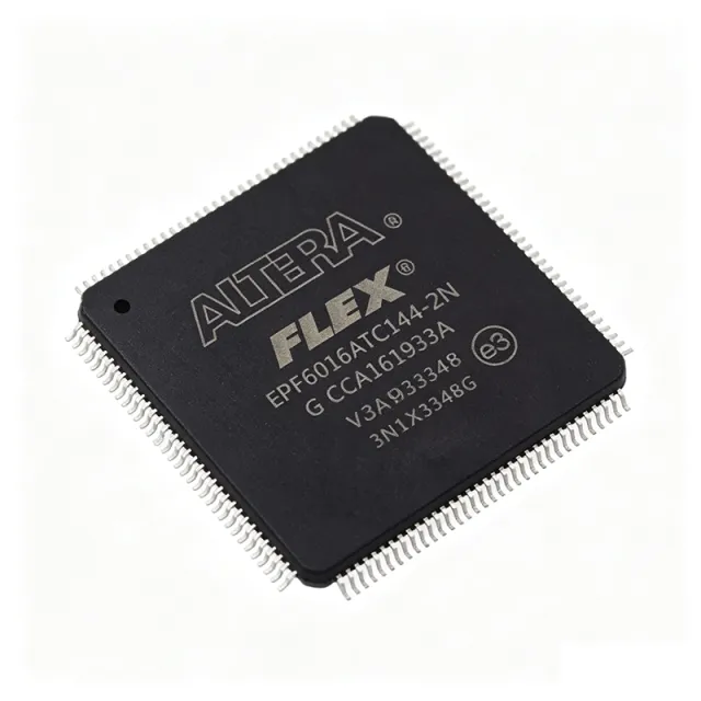
EPF6016AT1144-3N - FLEX 6000 FPGA 16K Gates | Altera TQFP-144
EPF6016AT1144-3N

EPF6016AT1144-3N - FLEX 6000 FPGA 16K Gates | Altera TQFP-144

The Altera (Intel) EPF6016AT1144-3N is a member of the FLEX 6000 family of SRAM-based programmable logic devices (PLDs), delivering approximately 16,000 typical gates in a 144-pin TQFP (T144) thin quad flat pack package. Built on a 0.42 µm CMOS SRAM process, the device integrates 1,320 logic elements (LEs), 16,000 typical gates, and a maximum of 132 user I/O pins operating at 3.3 V I/O with a 5.0 V tolerant input option. The "A" suffix designates the higher-performance -3 speed grade (commercial), optimized for medium-density glue logic, bus interfacing, and state-machine consolidation in cost-sensitive industrial, communications, and consumer designs. A field-programmable gate array (FPGA) is a semiconductor integrated circuit that engineers can configure after manufacturing to implement custom digital logic functions. FPGAs sit within the programmable logic hierarchy alongside CPLDs, PALs, and GALs, but offer higher logic density, distributed register-rich architectures, and on-chip SRAM configuration memory. The FLEX 6000 family specifically targets low-to-mid density glue-logic replacement of discrete 74-series TTL and 4000-series CMOS parts, while providing non-volatile in-system reconfigurability through external configuration memory (EPC2, EPC1441). Key features of the EPF6016AT1144-3N include 16,000 typical gates (24,000 maximum), 1,320 logic elements arranged in logic array blocks (LABs), 16,704 RAM bits distributed across embedded array blocks (EABs), and 132 user I/O pins. The device supports in-system programmability (ISP) via the ByteBlasterMV or BitBlaster download cable, multi-voltage I/O (MVIO) operation, and IEEE 1149.1 boundary-scan test (JTAG). The 144-pin TQFP package provides a robust plastic surface-mount footprint for industrial-temperature operation and automated assembly. The FLEX 6000 architecture employs a four-input look-up table (LUT) per logic element, fast carry chains for arithmetic operations, and dedicated cascade chains for wide fan-in functions. Each LE contains a programmable register that can be configured as D, T, JK, or SR flip-flop with independent clock, clock-enable, and clear/preset controls. Embedded array blocks (EABs) deliver up to 2,048 bits of dual-port RAM per block, supporting FIFO buffers, ROM look-ups, and arithmetic coefficient storage. The continuous FastTrack interconnect routes signals across all LABs and EABs with predictable, deterministic timing. Typical applications include industrial control and factory automation glue logic, telecommunications line-card bus interfaces, consumer electronics display controllers, networking peripheral bridges, and embedded system I/O expansion. The EPF6016AT1144-3N is also widely used in legacy PCI bus interfaces, microcontroller peripheral expansion, and as a configuration-memory controller in multi-FPGA systems. Its moderate density and low non-recurring engineering (NRE) cost make it an excellent choice for low-volume production or prototyping where ASIC conversion is not economically justified. When designing with this device, ensure the supply rails (VCCINT 3.3 V and VCCIO 3.3 V or 2.5 V) are decoupled with 0.1 µF ceramic capacitors placed within 6 mm of every VCC pin, and that the JTAG TCK signal is properly terminated to avoid configuration errors. Designers migrating from MAX 7000 or MAX 3000 CPLDs to FLEX 6000 should be aware that FLEX 6000 is SRAM-based and loses configuration on power-down, requiring an external configuration PROM such as the EPC2 or EPC1441. This page synthesizes FLEX 6000 family datasheet parameters, drop-in package-compatible alternatives from the same family, and practical design notes not found in distributor listings.

RFQ تماس
EPF6016ATC100-1 - FLEX 6000 FPGA, 16K Gates, 100-TQFP | Altera
EPF6016ATC100-1

EPF6016ATC100-1 - FLEX 6000 FPGA, 16K Gates, 100-TQFP | Altera

The Intel (formerly Altera) EPF6016ATC100-1 is a FLEX 6000 family Field-Programmable Gate Array (FPGA) containing approximately 16,000 gates, packaged in a 100-pin Thin Quad Flat Pack (TQFP) surface-mount package. The device integrates 1,320 logic elements (LEs) organized into 132 Logic Array Blocks (LABs) and provides 81 user I/O pins with an internal operating frequency up to 172 MHz, making it well suited for glue-logic, bus-interface, and high-volume gate-array replacement designs. A Field-Programmable Gate Array (FPGA) is a type of programmable logic device (PLD) that contains an array of configurable logic blocks (CLBs), programmable interconnect, and I/O cells, all of which can be reconfigured by the end user after manufacture. FPGAs sit in the broader hierarchy of digital integrated circuits as programmable logic -> logic ICs -> integrated circuits -> semiconductors. The FLEX 6000 family specifically targets low-cost, high-volume applications where the design flexibility of an FPGA is required but the very high gate counts of larger FLEX 10K or APEX families are unnecessary. Key features of the EPF6016ATC100-1 include 1,320 LEs distributed across 132 LABs, 81 available user I/O pins, an internal clock frequency ceiling of 172 MHz, in-system programmability via SRAM configuration cells, and multi-voltage I/O support. The "ATC" speed grade and -1 temperature suffix designate a commercial-temperature device (0°C to +85°C) in the standard AC speed bin, while the "100" package code indicates the 100-TQFP footprint. The device operates from a 3.3 V core supply and supports 5.0 V tolerant I/O, simplifying interface to legacy TTL logic. Architecturally, the FLEX 6000 family employs a continuous interconnect structure called the FastTrack that links every LAB to every other LAB through horizontal and vertical routing segments, providing predictable and fast signal propagation. Each LAB contains 10 LEs with a local interconnect, and each LE contains a 4-input look-up table (LUT), a programmable flip-flop, and dedicated carry/control logic for arithmetic and counter applications. The device stores its configuration in SRAM cells, which means it must be reconfigured at every power-up from a serial ROM or microcontroller. Typical applications for the EPF6016ATC100-1 include bus-bridging between microprocessors and peripherals, glue-logic replacement in telecommunications backplanes, custom state machines in industrial controllers, peripheral interface adapters, and prototyping of gate-array designs prior to ASIC conversion. Because the FLEX 6000 family was originally positioned as a low-cost programmable alternative to mask-programmed gate arrays, the EPF6016ATC100-1 is most often seen in legacy 3.3 V designs or as a hardware-revision-friendly replacement for discrete TTL/CMOS logic boards. When designing with this part, the engineer must allocate a configuration memory device (EPC2 or compatible) because the SRAM-based configuration is volatile. Additionally, all unused I/O pins should be left floating or driven to a defined state, and the JTAG chain should be considered for boundary-scan test access. The 100-TQFP package has a 14 mm x 14 mm body and is suitable for standard surface-mount assembly lines. This page synthesizes distributor pricing, drop-in alternatives drawn from the same FLEX 6000 family, and practical design notes not found on the manufacturer datasheet.

RFQ تماس
EPF6016ATC100-2 - FLEX 6000 FPGA, 16K Gates, 100-TQFP | Altera
EPF6016ATC100-2

EPF6016ATC100-2 - FLEX 6000 FPGA, 16K Gates, 100-TQFP | Altera

The Intel (formerly Altera) EPF6016ATC100-2 is a member of the FLEX 6000 family of SRAM-based CMOS Field Programmable Gate Arrays (FPGAs), delivering 16,000 usable gates with 1,320 logic elements (LEs) in a 100-pin Thin Quad Flat Pack (TQFP) package. The -2 speed grade places it in the mid-speed tier of the family, and the 'TC' suffix indicates a TQFP commercial-temperature package, while the '100' specifies the 100-pin TQFP footprint. An FPGA is a programmable logic device that lets designers implement custom digital circuits through software configuration rather than mask-programmed silicon. FPGAs occupy a tier above CPLDs (greater density, distributed RAM, richer I/O) and below structured ASICs (lower NRE cost, in-system reprogrammability). The FLEX 6000 family sits at the low-density end of Altera's legacy FPGA portfolio, suitable for glue logic, bus interfacing, and small state-machine designs that do not justify an ASIC. Key features include 16,000 typical gates (5,000 to 24,000 usable range), 1,320 logic elements organized as 132 Logic Array Blocks (LABs), 81 user I/O pins, and embedded SRAM. The device is built on a 5V-tolerant CMOS process with multi-volt I/O support. Configuration is performed via the serial Passive Serial (PS) or the JTAG-based Passive Parallel Synchronous (PPS) modes using the FLEX 6000 configuration bitstream format. Typical applications include bus-bridging and protocol-conversion glue logic in telecom backplane cards, industrial control and machine-interface adapters, point-of-sale and kiosk controllers, and legacy replacement of 74-series TTL logic on dense PCB assemblies. The 100-pin TQFP package is hand-solderable and easy to prototype, making the EPF6016ATC100-2 a common choice for low-volume industrial designs. When designing with this part, note that the FLEX 6000 is in mature production status under Intel PSG - last-time-buy notices are common, so secure lifecycle planning early. Provide clean 5V/3.3V rails with adequate bulk decoupling, and respect I/O banking rules when mixing TTL and CMOS interfaces. This page synthesizes distributor pricing, drop-in same-package alternatives from the EPF6016ATC100-x family, and PCB layout notes not found in the legacy datasheet.

RFQ تماس
EPF6016ATC100-2N - 16K Gates FLEX 6000 FPGA, 100-TQFP | Altera/Intel
EPF6016ATC100-2N

EPF6016ATC100-2N - 16K Gates FLEX 6000 FPGA, 100-TQFP | Altera/Intel

The Altera (now Intel) EPF6016ATC100-2N is a member of the FLEX 6000 family of Field Programmable Gate Arrays, offering 16,000 gates with 1,320 logic elements (cells) housed in a 100-pin TQFP package. The device operates at a maximum internal frequency of 172 MHz, is fabricated on a 0.42 µm CMOS process, and targets 3.3V core operation with 81 available user I/O pins. An FPGA (Field-Programmable Gate Array) is a type of programmable logic device that combines the flexibility of software-configurable hardware with the integration density of a custom ASIC. Within the broader semiconductor taxonomy, FPGAs sit alongside CPLDs and gate arrays in the programmable logic category, providing higher logic density than CPLDs and faster time-to-market than mask-programmed gate arrays. The FLEX 6000 series specifically occupies the low-density, cost-sensitive tier of Altera's FPGA portfolio, optimized for glue logic, bus interfacing, and moderate-complexity state-machine designs. Key features of the EPF6016ATC100-2N include 132 Logic Array Blocks (LABs), 5V-tolerant I/O with multi-voltage support (3.3V/5V), in-system programmability via a JTAG/IEEE 1149.1 interface, and a 4-input Look-Up Table (LUT) architecture. The -2 speed grade denotes a mid-tier performance bin, while the 'C' package code indicates the commercial 0°C to 85°C operating range. The 'N' suffix denotes lead-free / Pb-free assembly. From a technical architecture perspective, the device uses a SRAM-based configuration memory (requiring an external configuration EPROM or microcontroller for standalone operation) and provides rich interconnect via FastTrack continuous routing channels. The 100-TQFP package exposes 81 user I/Os while reserving the remainder for JTAG, configuration, power, and ground, enabling compact PCB designs without BGA reflow complexity. Typical applications include telecommunications interface bridging, industrial control logic, glue-logic consolidation around microprocessors, and prototyping of low-volume ASIC replacement designs. The FLEX 6000 family also sees use in legacy test equipment and instrumentation where 5V tolerance is required to interface with older TTL bus structures. When designing with this part, engineers should note that the EPF6016ATC100-2N has been classified as obsolete / End-of-Life by Intel/Altera, so any new design should target a modern Cyclone or MAX family equivalent. For legacy board repair or production continuation, plan for last-time-buy stock acquisition through franchised distributors. This page synthesizes distributor pricing, drop-in alternatives, and practical design notes not found on standalone datasheet portals, giving procurement and engineering teams a single consolidated reference for the EPF6016ATC100-2N.

RFQ تماس
EPF6016ATC100-3 - 16K Gate FLEX 6000 FPGA 81 I/O 100-TQFP | Intel
EPF6016ATC100-3

EPF6016ATC100-3 - 16K Gate FLEX 6000 FPGA 81 I/O 100-TQFP | Intel

The Intel (formerly Altera) EPF6016ATC100-3 is a FLEX 6000 family Field Programmable Gate Array delivering 16,000 usable gates and 1,320 logic elements in a 100-pin TQFP package, built on a 0.42 µm CMOS SRAM-based process and rated for 3.3V core operation with a -3 speed grade supporting up to 142.86 MHz internal frequency. FLEX 6000 is the product family classification for a category of SRAM-based, low-density FPGAs manufactured by Altera (now part of Intel). In the broader programmable logic taxonomy, FLEX 6000 sits below FLEX 8000/10K and above Classic EPLDs; FPGAs themselves are a sub-category of programmable logic devices (PLDs), which are digital semiconductors that can be reconfigured after manufacture to implement arbitrary logic functions. FLEX 6000 devices target glue-logic, bus-interface, and state-machine applications where higher-density FPGAs would be over-specified. Key specifications include 81 available user I/O pins, 1,320 logic cells (LEs), 16,000 typical gates, 4 embedded Logic Array Blocks (LABs) per row with FastTrack interconnect, and an internal operating frequency of 142.86 MHz with a -3 speed grade. The device operates from a 3.3V supply and supports in-system programmability via the IEEE 1149.1 JTAG interface and the Altera ByteBlaster or BitBlaster configuration paths. The EPF6016ATC100-3 uses a SRAM-based configuration memory, which means the design must be reloaded from a serial PROM or microcontroller at every power-up. The 0.42 µm process and 100-TQFP plastic package give it an industrial operating temperature of 0°C to 85°C. The architecture exposes dedicated carry chains for fast adders, a global clear signal, and an optimized 4-input LUT structure per logic element, which differentiates it from the smaller EPF6010 family. Typical applications include peripheral bus bridges, industrial control glue logic, prototype ASIC emulation, legacy PCI interface bridging, and low-density DSP state machines. The 100-TQFP footprint is well suited to through-hole-friendly rework on legacy PCBs, and the JTAG-based configuration path supports ISP (in-system programming) on manufacturing lines. When designing with this part, ensure the configuration PROM or microcontroller is sized for the EPF6016's bitstream, account for the SRAM volatility (no retention without power), and respect the 3.3V I/O bank limits when mixing with 5V peripherals. Designers migrating from the EPF6010 family gain extra I/O and logic capacity without changing the Quartus pin assignment flow. This page synthesizes distributor pricing, drop-in alternatives, and design notes that supplement the manufacturer datasheet and Quartus device handbook for the FLEX 6000 family.

RFQ تماس
EPF6016ATC100-3N - 16K Gates FLEX 6000 FPGA, 100-TQFP | Intel
EPF6016ATC100-3N

EPF6016ATC100-3N - 16K Gates FLEX 6000 FPGA, 100-TQFP | Intel

The Intel EPF6016ATC100-3N is a member of the FLEX 6000 family of SRAM-based Field Programmable Gate Arrays (FPGAs), featuring 16,000 typical gates, 1,320 logic elements (LEs), 81 user I/Os, and an internal operating frequency up to 142.86 MHz, housed in a 100-pin TQFP package. The device is fabricated on a 0.42 micrometer CMOS process, operates from a 3.3 V supply, and supports in-system programmability through the FLEX 6000 SRAM configuration architecture. What is an FPGA? A Field Programmable Gate Array is a programmable logic device that integrates configurable logic blocks (LBs), programmable interconnect, and programmable I/O cells on a single semiconductor die. FPGAs sit hierarchically between simple PLDs (CPLDs, GALs) and fixed-function ASICs, providing hardware-level parallelism with software-reconfigurable logic - making them ideal for glue logic, prototyping, low-volume production, and design changes late in the product cycle without respinning a board. Key features include 1,320 logic elements organized into 132 Logic Array Blocks (LABs) with carry and cascade chains for high-speed arithmetic and wide-input functions, 81 user I/O pins supporting multiple I/O standards, built-in JTAG boundary-scan test support, and an SRAM-based configuration cell that allows unlimited reconfiguration. The -3N speed grade places it in the moderate-performance tier of the FLEX 6000 family. Technically, the FLEX 6000 architecture uses a continuous routing structure called the FastTrack Interconnect, which provides predictable timing across the device. Each LE contains a 4-input look-up table (LUT), a programmable register, and dedicated paths for carry propagation (counters, adders) and cascade chains (wide comparators). Configuration is volatile - external memory or a configuration PROM is required at power-up, distinguishing FPGAs from non-volatile CPLDs. Typical applications include telecommunication interface bridging, industrial control glue logic, low-density glue-logic consolidation replacing 74-series TTL, simple state machines, and education/development platforms for digital design. The wide package availability (TQFP-100) makes it well-suited for hand-solderable prototypes and low-cost PCB designs. When designing with this part, note that the EPF6016ATC100-3N is now marked obsolete (EOL) per distributor data. New designs should consider the FLEX 10K, Cyclone, or MAX II families; this part remains in service primarily for legacy board maintenance and long-lifecycle industrial equipment. This page synthesizes distributor pricing, drop-in same-package alternatives from the FLEX 6000 family, and practical design notes not collected in any single manufacturer document.

RFQ تماس
EPF6016ATC144-1 - FLEX 6000 FPGA, 16K Gates, 1320 Cells, 144-LQFP | Altera (Intel)
EPF6016ATC144-1

EPF6016ATC144-1 - FLEX 6000 FPGA, 16K Gates, 1320 Cells, 144-LQFP | Altera (Intel)

The Altera (Intel) EPF6016ATC144-1 is a member of the FLEX 6000 family of SRAM-based Field Programmable Gate Arrays, integrating 16,000 typical gates and 1,320 logic cells into a 144-pin LQFP (Low-profile Quad Flat Pack) surface-mount package. The device uses 0.42 µm CMOS SRAM process technology, operates from a 3.3 V core supply, and supports user I/O voltages tolerant to 5.0 V, enabling glueless interface to legacy 5 V peripherals. The 'ATC' speed grade and '1' device suffix designate the slowest of three speed grades offered in the family, optimized for low power rather than maximum toggle rate. An FPGA (Field Programmable Gate Array) is a semiconductor device containing an array of configurable logic blocks (CLBs) connected by programmable interconnect, allowing designers to implement arbitrary digital logic without fabricating a custom ASIC. The FLEX 6000 family is positioned as a low-cost alternative to gate-array ASICs and is well suited to glue logic, bus bridging, and state-machine replacement on volume production boards where full Custom IC development cost is unjustified. Key features include 1,320 logic elements organized into 132 Logic Array Blocks (LABs), 117 user I/Os, built-in JTAG boundary-scan support, and four low-skew global clock networks. The EPF6016ATC144-1 also provides tri-state buffer control on every I/O, support for MultiVolt I/O interfacing, and configurability via serial or parallel EPROM/Flash configuration devices. Architecturally, the FLEX 6000 device uses an enhanced continuous-channel routing interconnect combined with four dedicated carry chains per LAB for high-speed arithmetic. The continuous routing architecture minimizes interconnect delay variance, allowing designers to predict worst-case propagation delay more reliably than segmented architectures. Typical applications include telecommunications line cards, industrial control glue logic, peripheral bus bridges, and low-volume ASIC replacement. The wide I/O count (117) suits 32-bit datapath bridges and address-decoding functions. When designing with this device, verify the configuration scheme (passive serial, active serial, or JTAG) and confirm ByteBlaster/MasterBlaster support in the Quartus MAX+PLUS II toolchain. Note that this part is end-of-life per Intel PSG. This page synthesizes distributor pricing, drop-in alternatives from the FLEX 6000 family and equivalent XAIPART-listed MPNs, and practical design notes not found in the legacy Altera datasheet.

RFQ تماس
EPF6016ATC144-1N - FLEX 6000 FPGA, 16K Gates, 144-TQFP | Intel
EPF6016ATC144-1N

EPF6016ATC144-1N - FLEX 6000 FPGA, 16K Gates, 144-TQFP | Intel

The Intel EPF6016ATC144-1N is a member of the FLEX 6000 family of Field-Programmable Gate Arrays (FPGAs), originally designed by Altera and now supported under the Intel Programmable Solutions Group. It delivers 16,000 typical gates with 1,320 logic elements (cells) in a 144-pin Thin Quad Flat Pack (TQFP) package, providing an ideal low-cost programmable alternative to high-volume gate array applications. According to manufacturer listings, the device supports 117 user I/O pins and is specified for commercial operating temperature (0°C to 85°C) with a 3.0V to 3.6V supply voltage range. An FPGA (Field-Programmable Gate Array) is a type of programmable logic device that allows designers to configure digital logic blocks and interconnect routing after manufacturing. FPGAs sit at the top of the programmable logic hierarchy: CPLD (Complex Programmable Logic Device) -> FPGA -> structured ASIC. The FLEX 6000 family was Altera's first SRAM-based FPGA family and represented a major step in low-cost, high-volume programmable logic, occupying the space between traditional CPLDs and high-density FLEX 10K FPGAs. Key features of the EPF6016ATC144-1N include: 1,320 logic elements, an internal frequency rating of up to 172 MHz, 117 user I/O pins, and SRAM-based configuration that supports in-system reprogramming. The 144-TQFP package uses a 20 mm × 20 mm body with 0.5 mm pitch gull-wing leads, making it compatible with standard SMT assembly lines. The device is built on a 0.42 µm CMOS process with 5 nm SRAM configuration cells, providing fast reconfiguration and unlimited reprogram cycles. The EPF6016ATC144-1N architecture combines Logic Array Blocks (LABs), Embedded Array Blocks (EABs) for memory functions, FastTrack interconnecting routing, and dedicated I/O cells with JTAG support. MultiVolt I/O allows interfacing with 3.3V and 5.0V logic. The device is programmed via the Altera ByteBlaster or BitBlaster download cable through a JTAG interface, and supports both serial and parallel configuration modes. Typical applications include glue logic replacement, high-volume gate-array prototyping, industrial control logic, communications interface bridging, and consumer electronics where fast design changes are required during prototyping or design testing. The wide commercial temperature range and moderate logic capacity make it suitable for cost-sensitive production runs. When designing with the EPF6016ATC144-1N, ensure adequate decoupling: place 0.1 µF and 10 µF capacitors close to each VCCINT and VCCIO pin. The 144-TQFP package requires careful PCB thermal management — at high toggle rates, junction temperature can rise significantly above ambient. Always configure unused I/O pins as inputs with bus-hold enabled or as outputs driving ground to minimize switching noise. This page synthesizes distributor pricing, drop-in alternatives, and practical design notes not found in the original Altera datasheet — giving engineers a single source for parametric comparison and supply-chain decisions on this legacy but still-relevant FPGA.

RFQ تماس
EPF6016ATC144-2 - FLEX 6000 FPGA, 16K Gates, 117 I/O | Intel
EPF6016ATC144-2

EPF6016ATC144-2 - FLEX 6000 FPGA, 16K Gates, 117 I/O | Intel

The Intel (formerly Altera) EPF6016ATC144-2 is a member of the FLEX 6000 family of SRAM-based reprogrammable FPGAs, delivering 16,000 typical gates (24,000 maximum logic elements) in a 144-pin LQFP (LFQFP) surface-mount package with 117 user I/Os. Built on a 0.30 µm CMOS SRAM process, the device combines 1,320 logic elements organized into 132 Logic Array Blocks (LABs), each containing 10 LEs connected by carry and cascade chains for high-speed arithmetic and wide-input functions. What is an FPGA? A Field-Programmable Gate Array (FPGA) is a semiconductor IC containing a matrix of configurable logic blocks (CLBs), programmable interconnect, and I/O cells, all defined by a user-supplied bitstream after manufacturing. FPGAs sit between fixed-function ASICs and software-driven processors in the digital-design hierarchy, offering hardware-timed parallelism, fast time-to-prototype, and field re-programmability for design iteration, algorithm acceleration, and glue-logic integration. The FLEX 6000 family targets low-to-mid density glue logic and is part of the broader programmable logic device (PLD) taxonomy. Key features of the EPF6016ATC144-2 include 117 user I/Os, 132 LABs, on-chip SRAM-based configuration memory, in-system programmability via JTAG (IEEE 1149.1), and support for Altera MAX+PLUS II and Quartus design flows. The device operates from a single supply voltage and supports the commercial temperature grade. Carry chains support high-speed arithmetic functions such as counters and adders, while cascade chains implement wide-input functions with minimum delay. Dedicated clock pins and global routing enable deterministic timing for synchronous designs. The EPF6010/EPF6016 family uses the OptiFLEX architecture with continuous horizontal routing across rows and vertical routing in columns, balancing density and routability for designs up to ~16K gates. The architecture supports LPM, VHDL, Verilog HDL, and EDIF 2.0/3.0 design entry, allowing seamless integration with third-party EDA synthesis and simulation tools. Internal configuration memory is volatile and must be loaded from an external serial or parallel PROM at power-up, or via JTAG. Typical applications for the EPF6016ATC144-2 include glue logic for industrial control boards, I/O expansion and bus interfacing, prototyping of mid-density digital designs, replacement of discrete TTL/CMOS logic, custom peripheral controllers in embedded systems, and educational platforms teaching FPGA design with MAX+PLUS II. The 117 I/Os make it suitable for designs with moderate I/O count, while the 144-pin LQFP package simplifies PCB assembly with standard surface-mount equipment. When designing with this device, consider that configuration memory is volatile - a serial configuration EPROM (e.g., EPC2, EPC4) is required to load the bitstream on power-up, or JTAG can be used for prototype programming. The 144-pin LQFP package has a 0.5 mm pin pitch and requires careful PCB layout for signal integrity. Decoupling capacitors (0.1 µF and 10 µF) should be placed adjacent to every supply pin to minimize switching noise. This page synthesizes distributor pricing, lifecycle data, drop-in package-compatible alternatives from the FLEX 6000/10K family, and practical design notes not found in the manufacturer datasheet alone, helping engineers select the right pin-compatible FPGA for legacy or new designs.

USD $13.85 تماس
EPF6016ATC144-2N - FLEX 6000 FPGA, 16K Gates, 1320 Cells | Intel
EPF6016ATC144-2N

EPF6016ATC144-2N - FLEX 6000 FPGA, 16K Gates, 1320 Cells | Intel

The Intel (formerly Altera) EPF6016ATC144-2N is a member of the FLEX 6000 family of SRAM-based, reprogrammable CMOS Field Programmable Gate Arrays, offering 16,000 typical gates (24,000 maximum logic elements) and 1,320 logic cells in a 144-pin TQFP package. The device integrates 132 Logic Array Blocks (LABs), 117 user I/O pins, and operates from a 3.3 V core supply with MultiVolt I/O supporting 3.3 V and 5.0 V interfaces. Internal performance supports system speeds up to 166.67 MHz, and the part is fabricated on a 0.42 µm CMOS process. A Field Programmable Gate Array (FPGA) is a semiconductor device built around an array of configurable logic blocks (CLBs / LEs), programmable routing interconnect, and I/O cells, that can be re-programmed in-system to implement arbitrary digital logic functions. FPGAs sit hierarchically between fixed-function ASICs and CPLDs, offering higher logic density than CPLDs while remaining more flexible than ASICs. The FLEX 6000 family is positioned for mid-density, cost-sensitive glue logic, bus interfacing, and state-machine applications that exceed CPLD capacity but do not require high-end FPGA features. Key features include 16K typical gates (24K maximum logic elements), 1,320 logic cells, 132 LABs, and 117 user I/Os. The device supports in-system programmability via the IEEE 1149.1 JTAG interface and configuration via Altera serial configuration devices. Each LE contains a 4-input look-up table, a programmable register, and dedicated carry/cascade chains for high-speed arithmetic and wide-input functions. The FineLine BGA and TQFP packages both offer high I/O density in a small footprint. Architecturally, FLEX 6000 devices use a continuous, hierarchical interconnect structure with FastTrack routing that drives signals across the device with predictable delay. The 0.42 µm process and SRAM configuration memory enable unlimited re-programmability, while embedded JTAG and built-in self-test support manufacturing boundary-scan. Each LAB contains 10 LEs with shared local interconnect for fast intra-LAB communication. Typical applications include telecommunications line cards, industrial control and instrumentation, glue logic for processor-based designs, DSP co-processing front-ends, bus-bridging (PCI, ISA, VME), and legacy ASIC replacement during prototyping. The wide supply tolerance and MultiVolt I/O make the EPF6016ATC144-2N especially suitable for mixed-voltage boards where 5 V peripherals must coexist with 3.3 V logic. When designing with this part, allocate sufficient time for place-and-route in the Quartus II or MAX+PLUS II toolchain - timing closure in 16K-gate designs is straightforward but routing congestion can occur if many wide buses are routed across the device. Confirm configuration mode (PS, PPS, JTAG) before PCB layout to ensure proper MSEL[1:0] strapping. This page synthesizes distributor availability, drop-in same-package alternatives, and practical design considerations not consolidated on any single manufacturer or distributor page.

RFQ تماس
EPF6016ATC144-3 - FLEX 6000 FPGA, 16K Gates, 1320 Cells | Intel
EPF6016ATC144-3

EPF6016ATC144-3 - FLEX 6000 FPGA, 16K Gates, 1320 Cells | Intel

The Intel EPF6016ATC144-3 is a FLEX 6000 family Field Programmable Gate Array (FPGA) integrating 16,000 gates, 1,320 logic cells, and 117 user I/Os in a 144-pin TQFP package with -3 (faster) speed grade. Built on a 0.42 µm CMOS SRAM-look-up-table architecture, the device operates from a 3.3 V core supply (VCCINT) and supports 2.5 V / 3.3 V / 5.0 V I/O via VCCIO banking. A Field Programmable Gate Array (FPGA) is a semiconductor device built around an array of configurable logic blocks (CLBs), programmable interconnect, and I/O cells, all customized via SRAM-based configuration memory. FPGAs sit within the broader Programmable Logic hierarchy: PLD -> CPLD -> FPGA -> SoC FPGA, and serve as the lowest-cost / lowest-power option for glue logic, bus bridging, and low-density state-machine replacement compared with higher-density families. Key features include 132 Logic Array Blocks (LABs) each containing 10 Logic Elements (LEs), dedicated carry and cascade chains for high-speed arithmetic and wide input functions, embedded IEEE 1149.1 JTAG boundary-scan support, and an in-system programmability (ISP) interface. The TQFP-144 footprint is shared across most FLEX 6000 densities via Altera's SameFrame pin-compatibility program, allowing designers to migrate designs across density points without PCB rework. Architecturally, the FLEX 6000 uses a continuous, hierarchical interconnect network (FastTrack) that delivers predictable timing across the device. The -3 speed grade targets internal frequencies up to 142.86 MHz, suitable for peripheral bus bridges, custom peripherals, and reconfigurable I/O expansion. The SRAM configuration cell requires a configuration device (e.g., EPC2) or JTAG download at every power-up. Typical applications include glue-logic integration in telecom line cards, industrial control boards, and legacy peripheral bus (PCI, ISA) bridge implementations, where its low cost and moderate density outperform mask-programmed gate arrays for low- to mid-volume production. The part is also used for prototyping where rapid design iteration is required. When designing with the EPF6016ATC144-3, ensure VCCINT is tied to 3.3 V and VCCIO is matched to the connected bus voltage; mismatched rails will damage I/O buffers. Also allocate a configuration PROM (EPC2, EPC4) or JTAG header for in-system programming - the device has no on-chip non-volatile memory. This page synthesizes distributor pricing, SameFrame drop-in alternatives within the FLEX 6000 family, and practical design notes not aggregated on the manufacturer datasheet.

RFQ تماس
EPF6016ATC144-3N - FLEX 6000 FPGA 16K Gates 1320 Cells TQFP-144
EPF6016ATC144-3N

EPF6016ATC144-3N - FLEX 6000 FPGA 16K Gates 1320 Cells TQFP-144

The Intel (formerly Altera) EPF6016ATC144-3N is a member of the FLEX 6000 family of Field Programmable Gate Arrays (FPGAs) built on the OptiFLEX architecture, delivering approximately 16,000 gates and 1,320 logic elements in a 144-pin TQFP package. The device operates at a maximum internal frequency of 142.86 MHz, supports 117 user I/O pins, and is fabricated on a 0.42 micron CMOS process running at 3.3 V core supply. An FPGA (Field Programmable Gate Array) is a type of programmable logic device (PLD) that allows designers to implement custom digital logic circuits by configuring an array of configurable logic blocks (CLBs), programmable interconnects, and I/O cells after manufacture. FPGAs sit above CPLDs and gate arrays in the programmable logic hierarchy, offering higher logic density, finer-grained parallelism, and on-chip memory. The FLEX 6000 family specifically targets low-cost, high-volume designs that previously required fixed gate arrays, providing fast design iteration during prototyping. Key features of the EPF6016ATC144-3N include 1,320 logic elements (132 LABs/Logic Array Blocks), 117 user I/O pins, embedded SRAM configuration memory (SRAM-based, volatile configuration requiring external configuration device), in-system programmability via JTAG, and a speed grade of -3 indicating the commercial high-performance tier. The TQFP-144 package exposes all major interface signals including dedicated clock inputs, JTAG, and configuration pins. The OptiFLEX architecture minimizes die size through continuous, segmented routing resources interleaved with Logic Array Blocks. Each LAB contains ten logic elements with 4-input look-up tables (LUTs), a carry chain for arithmetic, and a cascade chain for wide fan-in functions. The device supports true dual-port and single-port embedded memory blocks for FIFO and register-file applications, plus dedicated I/O registers for high-speed source-synchronous interfaces. Typical applications for the EPF6016ATC144-3N include glue logic integration in telecommunications line cards, industrial control and factory automation controllers, low-cost replacement for fixed gate arrays in high-volume consumer products, bridge and protocol conversion between legacy peripherals, and educational or prototyping platforms where designers need a robust, mature, programmable logic fabric. The 117 available I/Os support a wide range of parallel bus widths and mixed-signal interface requirements. When designing with this device, note that the FLEX 6000 family uses SRAM configuration cells, so the bitstream must be reloaded from an external serial or parallel configuration PROM (such as the EPC2 or EPC8) on every power-up. Plan board layout to keep the 144-pin TQFP decoupling network within the inductance budget and to ensure JTAG chain access for in-system programming. This page synthesizes distributor pricing, drop-in same-package alternatives drawn from the FLEX 6000 family, and practical design notes not found in the original manufacturer datasheet.

RFQ تماس
EPF6016ATC144-3S - FLEX 6000 FPGA, 132 LABs, 117 IOs | Intel
EPF6016ATC144-3S

EPF6016ATC144-3S - FLEX 6000 FPGA, 132 LABs, 117 IOs | Intel

The Intel (formerly Altera) EPF6016ATC144-3S is a member of the FLEX 6000 family of Field Programmable Gate Arrays (FPGAs), delivering 16,000 typical gates (24,000 maximum system gates) in a 144-pin TQFP (Thin Quad Flat Pack) package. It provides 1,320 logic elements distributed across 132 Logic Array Blocks (LABs) with 117 user I/O pins, an internal frequency of 172 MHz, and is built on a 0.42 µm CMOS SRAM process with 5.0 V core voltage. A Field Programmable Gate Array (FPGA) is a type of integrated circuit that can be configured by the customer or designer after manufacturing, hence the term field-programmable. The FLEX 6000 family sits within Intel's programmable logic hierarchy between simpler Complex Programmable Logic Devices (CPLDs) and higher-density FPGAs such as the FLEX 10K and APEX families. FPGAs in general belong to the broader semiconductor taxonomy of Programmable Logic Devices (PLDs), which also include SPLDs and CPLDs. They are widely used for digital logic prototyping, glue logic, custom I/O interfacing, and pre-ASIC design verification where production volumes do not yet justify a mask-programmed gate array. The EPF6016ATC144-3S is specified as commercial grade with an operating temperature range of 0°C to 85°C and operates from a 5.0 V supply. The trailing S in the order code denotes a specific Altera/Intel ordering suffix (often indicating a particular shipment form or speed/packaging variant), while the -3 speed grade denotes the -3 performance bin within the FLEX 6000 family. The part supports in-system programmability via the IEEE 1149.1 (JTAG) boundary-scan interface and is configured via a serial configuration device. Typical applications for the EPF6016ATC144-3S include glue logic in telecom infrastructure, industrial control and factory automation I/O expansion, PCI bus interface bridging, custom peripheral controllers in embedded systems, and pre-ASIC prototyping where design teams need to validate RTL prior to tape-out. The 117 available user I/Os make the device well-suited to bridging legacy 5 V peripherals to modern ASICs or microprocessors. When designing with this part, ensure that all 5 V supply rails are properly decoupled with 0.1 µF ceramic capacitors placed within 5 mm of each VCC pin, and that JTAG chain integrity is verified before configuration. The device is now considered legacy/NRND: production of the FLEX 6000 family has largely ended, and Intel recommends migrating to Cyclone-series devices for new designs. This page synthesizes distributor pricing, drop-in package-compatible variants from the same FLEX 6000 family, and practical design notes not found on a single distributor page.

RFQ تماس
EPF6016ATI100-2 - FLEX 6000 FPGA 16K Gates 81 I/O 100-TQFP | Altera
EPF6016ATI100-2

EPF6016ATI100-2 - FLEX 6000 FPGA 16K Gates 81 I/O 100-TQFP | Altera

The Altera (Intel Programmable Solutions Group) EPF6016ATI100-2 is a member of the FLEX 6000 family of SRAM-based, low-cost Field Programmable Gate Arrays (FPGAs) offering 16,000 equivalent gates, 1,320 logic elements, and 81 user I/O pins in a 100-pin TQFP surface-mount package. The device operates from a 3.3 V supply (3.0 V to 3.6 V), is built on a 0.42 µm CMOS process, and supports an internal frequency of up to 166.67 MHz, making it suitable for high-volume glue-logic and gate-array replacement designs. An FPGA (Field Programmable Gate Array) is a type of programmable logic device (PLD) that combines the high integration of a gate array with the design flexibility of in-system programmability. In the broader system hierarchy, the FLEX 6000 family sits between simple SPLDs/CPLDs and high-density SRAM-based FPGAs such as the FLEX 10K and APEX families, targeting cost-sensitive applications that previously required fixed gate arrays. The FLEX 6000 architecture uses Look-Up Tables (LUTs), embedded array blocks (EABs), and FastTrack interconnect to deliver deterministic timing at low cost. Key features of the EPF6016ATI100-2 include 132 LABs (Logic Array Blocks), an industrial operating temperature range of 0°C to 85°C (commercial) per the distributor datasheet, and FineLine BGA-compatible pin assignments in the 100-TQFP variant. The "I" suffix indicates the industrial temperature grade, while the "-2" speed grade designates a mid-range performance bin. The device is configured via a serial EPROM or microcontroller and supports in-system programmability through the JTAG IEEE 1149.1 boundary-scan interface. Typical applications include peripheral interface bridging, custom bus controllers, glue logic in telecom and networking equipment, low-volume ASIC replacement, and rapid prototyping of digital systems. The EPF6016ATI100-2 provides an ideal low-cost, programmable alternative to high-volume gate array designs, allowing fast design changes during prototyping or production testing. When designing with this FPGA, plan for external configuration memory (typically an EPC2 or EPC16 serial configuration device) and ensure all I/O banks are powered within the 3.0 V to 3.6 V range. This page synthesizes distributor inventory data, cross-references, and engineering trade-offs that the manufacturer datasheet alone does not provide.

RFQ تماس
EPF6016ATI100-2N - FLEX 6000 FPGA, 16K Gates, 100-TQFP | Altera/Intel
EPF6016ATI100-2N

EPF6016ATI100-2N - FLEX 6000 FPGA, 16K Gates, 100-TQFP | Altera/Intel

The Intel/Altera EPF6016ATI100-2N is a member of the FLEX 6000 family of SRAM-based Field Programmable Gate Arrays (FPGAs), delivering approximately 16,000 usable gates in a 100-pin TQFP (Thin Quad Flat Pack) package. The device is built on a 0.42 um CMOS SRAM process and contains 1,320 logic elements (LEs) organized into 132 Logic Array Blocks (LABs), with 81 user I/O pins and an internal maximum operating frequency of approximately 166.67 MHz at a 3.3 V core supply. It supports in-system configuration via a JTAG-compatible boundary-scan interface and provides setup times as low as 2 ns with 0 ns hold time for high-speed sequential logic. An FPGA (Field Programmable Gate Array) is a type of integrated circuit containing an array of configurable logic blocks (CLBs), programmable interconnect, and I/O cells that can be reconfigured by the designer after manufacturing. FPGAs sit between fixed-function ASICs and software-programmable processors in the design hierarchy, offering hardware-level parallelism without the NRE cost of an ASIC. The FLEX 6000 family specifically targets low-cost, high-volume glue logic, control, and bus-interface applications where fast design changes during development are required. Key features of the EPF6016ATI100-2N include 81 user I/Os, JTAG BST (Boundary-Scan Test) support, slew-rate control on output buffers, tri-state buffer capability per I/O, and dedicated clock networks. The LABs each contain 10 LEs, and the FastTrack interconnect provides predictable timing paths between LABs. I/O pins can drive LE registers directly via the row and column interconnect, simplifying timing closure for high-speed state machines and FIFO controllers. Architecturally, the device combines a fine-grained LE structure with row/column interconnect routing, allowing automatic place-and-route via the MAX+PLUS II or Quartus design tools. The 0.42 um SRAM process supports 5.0 V tolerant I/Os when the device is powered at 3.3 V, useful for mixed-voltage bus bridging between legacy 5 V peripherals and 3.3 V processors. Typical applications include bus bridging between microprocessors and peripherals, custom peripheral glue logic in embedded systems, ASIC prototyping, state-machine controllers, and pre-production design validation. The wide I/O count supports 8/16/32-bit data buses with handshake signals. When designing, ensure the configuration EPROM (such as an EPC2 or EPC8) is correctly sized for the bitstream, and observe 3.3 V supply decoupling with at least 0.1 uF ceramic capacitors near each VCC pin to maintain signal integrity on the JTAG and high-speed I/O lines. This page combines distributor pricing, verified drop-in alternatives, and practical design notes that supplement the manufacturer datasheet for sourcing and redesign decisions.

RFQ تماس
EPF6016ATI144-2 - FLEX 6000 FPGA 16K Gates | Altera
EPF6016ATI144-2

EPF6016ATI144-2 - FLEX 6000 FPGA 16K Gates | Altera

The Altera EPF6016ATI144-2 is a member of the FLEX 6000 family of SRAM-based programmable logic devices, providing 16K typical gates (1,320 logic elements/registers), 117 user I/O pins, and a maximum internal clock frequency of 153 MHz in a 144-pin TQFP package. It is fabricated on a 0.42 µm CMOS process and operates from a single 3.3 V supply (3.0 V to 3.6 V) with 5.0 V tolerant I/O. A Field Programmable Gate Array (FPGA) is a type of programmable logic device (PLD) that combines an array of configurable logic blocks (CLBs), programmable routing, and I/O cells on a single die. Within the broader semiconductor hierarchy, an FPGA belongs to the digital logic IC family, alongside ASICs, CPLDs, and microcontrollers, and is favored for medium-volume glue-logic, prototyping, and pre-ASIC validation. The FLEX 6000 family specifically targets low-cost, register-rich, LUT-based designs as an alternative to gate arrays. Key features include OptiFLEX architecture with embedded memory blocks, four dedicated clock inputs and a global clock network, JTAG (IEEE Std 1149.1) boundary-scan support, in-system programmability via the serial configuration EPROM interface, and per-pin 5.0 V tolerance with PCI-clamp diodes. The -2 speed grade is the mid-tier offering of the family, sitting between the -1 (slowest) and -3 (fastest) grades. The EPF6016ATI144-2 is built on a 0.42 µm SRAM cell, providing volatile configuration that must be loaded at every power-up from an external EPROM or microcontroller. The -A speed/power descriptor denotes the industrial temperature grade (-40 °C to 100 °C) in the TQFP-144 footprint, and the I indicates an industrial temperature range variant. Typical applications include industrial control glue logic, PCI interface bridges, telecommunications line cards, and prototyping for ASIC designs. The high I/O count (117) makes it well-suited for bus-intensive designs such as 32-bit microprocessor interfaces. It is also widely used in legacy telecom backplane designs where long-term availability and pin compatibility with the FLEX 6000 family are required. When designing with this device, ensure that a configuration EPROM (such as EPC2 or EPC8) is used because the SRAM cells are volatile, and verify that the Quartus II / MAX+PLUS II toolchain (legacy support) supports the targeted -2 speed grade. Designers migrating from -2 to -3 grades must re-time their designs, as internal delays scale with the speed grade. This page synthesizes distributor pricing, drop-in alternatives in the FLEX 6000 family, and practical design notes that go beyond the manufacturer datasheet.

RFQ تماس
EPF6016ATI144-2N - FLEX 6000 FPGA 16K Gates 1320 LEs | Altera
EPF6016ATI144-2N

EPF6016ATI144-2N - FLEX 6000 FPGA 16K Gates 1320 LEs | Altera

The Intel (formerly Altera) EPF6016ATI144-2N is a FLEX 6000 family Field-Programmable Gate Array (FPGA) integrating 16,000 gates and 1,320 logic elements, fabricated on a 0.42 µm CMOS process and housed in a 144-pin TQFP package with 117 user I/O lines and 4 dedicated inputs. A Field-Programmable Gate Array (FPGA) is a programmable logic device that combines the integration density of a gate array with the design flexibility of in-system reprogrammability. Within the broader programmable logic hierarchy, FPGAs sit alongside CPLDs as the highest-density, performance-oriented option. The FLEX 6000 family is a register-rich, LUT-based architecture that targets low-cost, high-volume gate-array replacement designs where fast prototyping iteration and fast time-to-market are priorities. Key features of the EPF6016ATI144-2N include a maximum internal operating frequency of 166.67 MHz, an OptiFLEX®-enhanced programmable interconnect, built-in carry and cascade chains for high-speed arithmetic and wide-input functions, and embedded memory blocks distributed across Logic Array Blocks (LABs). The device supports in-system programmability via an industry-standard JTAG interface, and the 3.3 V core supply (VCCINT) with 3.0 V–3.6 V tolerance enables low-power operation compared to 5.0-V-only predecessors. Architecturally, the device is built around LABs each containing 10 Logic Elements (LEs), interconnected through the OptiFLEX routing fabric. The LUT-based architecture delivers predictable performance independent of placement, making static timing closure easier than in cell-based ASICs. The I/O structure supports 5.0-V tolerant inputs when VCCIO is biased at 3.3 V, simplifying mixed-voltage board designs. Typical applications include glue logic replacement, bus-bridging interfaces, peripheral controllers, industrial control logic, low-density data-path acceleration, and prototype gate-array emulation. Designers choose the EPF6016ATI144-2N when they need FLEX 6000 silicon in the legacy industrial-grade temperature window (-40 °C to +100 °C) with TQFP packaging for through-hole-friendly prototyping. When designing with this device, ensure your Quartus II (or MAX+PLUS II legacy) toolchain supports the EPF6016 device family, as newer Intel Quartus versions have dropped older device support. Verify VCCINT and VCCIO decoupling with 0.1 µF + bulk capacitors placed adjacent to all supply pins. This page synthesizes distributor pricing tiers, drop-in FLEX 6000 family alternatives, parametric comparison tables, and practical design notes that go beyond the information available on a single manufacturer datasheet — helping engineers select and source the right FLEX 6000 FPGA quickly.

RFQ تماس
EPF6016ATI144-3 - FLEX 6000 FPGA, 132 LABs, 117 I/O, 144-LQFP | Intel
EPF6016ATI144-3

EPF6016ATI144-3 - FLEX 6000 FPGA, 132 LABs, 117 I/O, 144-LQFP | Intel

The Intel EPF6016ATI144-3 is a member of the FLEX 6000 family of Field Programmable Gate Arrays, featuring 1320 logic elements (LEs), 132 Logic Array Blocks (LABs), and 117 user I/O pins, housed in a 144-pin LQFP package. The device operates at up to 142.86 MHz and is built on a 3.3V CMOS process optimized for low-cost, high-volume designs. The "TI" suffix denotes an industrial temperature range (TJ from -40C to +100C), and the "-3" speed grade indicates a standard performance tier within the family. A Field Programmable Gate Array (FPGA) is a type of programmable logic device (PLD) that allows designers to implement custom digital logic through configuration rather than fixed silicon. The FLEX 6000 family sits within Intel's PLD hierarchy: PLD -> SRAM-based FPGA -> FLEX 6000 series -> EPF6016 sub-family. FPGAs enable rapid prototyping, hardware-level parallelism, and post-manufacture design changes that ASICs cannot offer, making them ideal for glue logic, interface bridging, and small-to-medium digital systems. Key features of the EPF6016ATI144-3 include 16,000 typical gates, a 4-input Look-Up Table (LUT) architecture, SRAM-based configuration memory, multiVolt I/O support for interfacing with 5.0V, 3.3V, and 2.5V devices, and JTAG-compliant boundary-scan testing (IEEE Std. 1149.1). The device also offers in-system programmability (ISP) via the JTAG port or the dedicated configuration interface, allowing field upgrades without removing the part from the board. Architecturally, the FLEX 6000 series uses an SRAM-based 4-input LUT fabric with embedded memory and routing interconnect, providing a balance of logic density and predictable timing. The 144-LQFP package offers 117 usable I/O pins after accounting for power, ground, configuration, and JTAG pins. The "I" in the part number indicates the industrial operating range, and the speed grade "-3" places this part in the standard-performance tier. Typical applications include telecommunications interface cards, industrial control and glue logic, legacy digital system prototyping, glue logic between microcontrollers and peripherals, parallel bus interfaces, and state-machine controllers. The 117 user I/O count and 142.86 MHz Fmax support moderate-complexity designs that require parallel processing or multiple parallel interfaces. When designing with this device, note that configuration data must be loaded from an external serial or parallel PROM at power-up because FLEX 6000 devices are SRAM-based and lose configuration when power is removed. Power sequencing, decoupling, and JTAG chain integrity are critical design considerations. This part is marked as obsolete on distributor channels - design for longevity by sourcing authorized stock or planning a migration to the MAX II or Cyclone equivalent families.

RFQ تماس
EPF6016ATI144-3N - FLEX 6000 FPGA 16K Gates 117 I/O | Altera / Intel
EPF6016ATI144-3N

EPF6016ATI144-3N - FLEX 6000 FPGA 16K Gates 117 I/O | Altera / Intel

The Altera (now Intel) EPF6016ATI144-3N is a member of the FLEX 6000 family of Field Programmable Gate Arrays (FPGAs) manufactured on a 0.42 µm CMOS process, integrating 16,000 gates (1,320 logic elements / 132 LABs) with 117 user I/O in a 144-pin TQFP (Thin Quad Flat Pack) package. Operating from a 3.3 V core supply, the device supports internal operation up to 142.86 MHz and provides SRAM-based configuration that can be loaded from a PROM or in-system via JTAG, enabling rapid design iteration. The "-3" speed grade combined with the industrial temperature range (-40 °C to +85 °C, suffix "I") and lead-free ("N") designation positions this part for mainstream industrial and telecom glue-logic applications. A Field Programmable Gate Array (FPGA) is a type of programmable logic device (PLD) — itself a category of integrated circuit — that uses configurable logic blocks (LBs), programmable interconnect, and programmable I/O cells to implement arbitrary digital circuits after fabrication. FPGAs sit at the top of the programmable logic hierarchy: ASIC < Gate Array < CPLD < FPGA. The FLEX 6000 family represents Altera's mid-1990s cost-optimized SRAM FPGA architecture, positioned between their Classic and FLEX 10K families, and remains in long-term supply for industrial and aerospace refresh programs. Key features include 1,320 logic elements arranged in 132 Logic Array Blocks (LABs), 117 user I/O pins, embedded JTAG (IEEE 1149.1) boundary-scan support, and four dedicated inputs. The architecture is built around SRAM configuration cells with 4-input look-up tables (LUTs), per-LAB carry chains for fast arithmetic, and a continuous routing matrix. The device is in-system programmable through the ByteBlaster or BitBlaster download cables, supporting rapid prototyping and field upgrades without removing the part from the board. Typical applications include industrial control glue logic, telecom interface bridging, motor control peripheral integration, legacy M68000/i960 co-processor glue, and avionics display controllers where the FLEX 6000 family has established long-term qualified status. The 144-pin TQFP package exposes 117 user I/O, which is sufficient for wide parallel buses plus multiple serial channels in bridge applications. When designing with this device, pay attention to the JTAG chain order — the EPF6016 shares a JTAG bus with other Altera legacy parts (FLEX 10K, MAX 7000) and must be ordered correctly when multi-device programming is used. Decoupling requires 0.1 µF and 10 µF capacitors per VCCINT and VCCIO pin group; the device is sensitive to supply droop during configuration. Always validate the configuration PROM or in-system flash image against the Quartus II 13.0 service pack release, which is the last officially supported design software for the FLEX 6000 family. This page synthesizes distributor pricing, drop-in alternatives from the Altera FLEX 6000 family, and practical design notes not found in the manufacturer datasheet alone.

RFQ تماس
EPF6016BC256-2 - FLEX 6000 FPGA, 16K Gates, 204 I/O | Altera
EPF6016BC256-2

EPF6016BC256-2 - FLEX 6000 FPGA, 16K Gates, 204 I/O | Altera

The Altera (now Intel) EPF6016BC256-2 is a member of the FLEX 6000 family of SRAM-based Field-Programmable Gate Arrays (FPGAs) housed in a 256-ball FineLine BGA package. It integrates 16,000 typical gates (24,000 maximum logic elements) and provides 204 user I/O pins across 1,320 logic elements, with a 5V-tolerant I/O architecture supplied from a 4.75V to 5.25V core and I/O rail. The '-2' suffix denotes the speed grade, optimized for higher internal performance versus '-1' while keeping cost lower than '-3'. A Field-Programmable Gate Array (FPGA) is a programmable logic device that combines programmable logic elements, configurable interconnect, and I/O blocks into a single silicon die. FPGAs sit above CPLDs in the programmable logic hierarchy and below ASICs in NRE cost; SRAM-based devices like the FLEX 6000 family are reconfigurable in-system, allowing rapid prototyping, field updates, and design reuse across product revisions without retooling. Key features include up to 1320 logic elements, 204 user I/Os, embedded array blocks for memory implementation, and JTAG-based in-system programmability via the IEEE 1149.1 boundary-scan interface. The device operates across the commercial 0C to 85C temperature range and supports fast synchronous state machines, register-intensive datapaths, and glue-logic replacement. The FLEX 6000 architecture is built on a 0.42-micron SRAM process with a four-input look-up table (LUT) per logic element and a continuous FastTrack interconnect. This delivers predictable timing, low static power, and deterministic place-and-route results - ideal for bus-interface bridging, peripheral controllers, and custom I/O expansion. Typical applications include industrial glue-logic, communication bridging between legacy microcontrollers and modern peripherals, ASIC prototyping, low-volume custom controllers, and DSP co-processing front-ends. The 204 I/O count makes it well-suited for parallel bus interfacing and bus-width conversion. When designing with this FPGA, ensure the 5V VCCIO and VCCINT rails share a clean power source and that decoupling follows the reference design. Quartus II (legacy) or MAX+PLUS II toolchains are used for place-and-route, and JTAG programming requires the ByteBlasterMV download cable. This page synthesizes distributor pricing, same-package drop-in alternatives, and practical design notes not found on the manufacturer datasheet alone - providing engineers with the cross-reference intelligence needed to manage the FLEX 6000 lifecycle.

RFQ تماس
EPF6016BC256-3 - 16K Gates FLEX 6000 FPGA, 256-BGA | Intel
EPF6016BC256-3

EPF6016BC256-3 - 16K Gates FLEX 6000 FPGA, 256-BGA | Intel

The Intel EPF6016BC256-3 is a member of the FLEX 6000 family of programmable logic devices, delivering 16,000 usable gates (13,200 typical logic elements) in a 256-ball FineLine BGA package. The device is fabricated on a 0.42 µm CMOS SRAM process and supports 204 user I/O pins, making it well suited for high-I/O glue-logic, bus-interface, and state-machine designs that have outgrown a CPLD but do not justify a larger FPGA. What is an FPGA? A Field-Programmable Gate Array (FPGA) is a semiconductor IC containing an array of configurable logic blocks (CLBs), programmable routing, and I/O cells that the user can define after manufacture via a configuration bitstream. FPGAs sit between simple PLDs/CPLDs (limited logic, deterministic timing) and ASICs (high NRE, long lead time). The FLEX 6000 family in particular targets cost-sensitive, high-volume applications such as consumer electronics, communications glue logic, and peripheral bridging - offering ASIC-like integration with the fast time-to-market of programmable logic. Key features of the EPF6016BC256-3 include a maximum internal frequency of 172 MHz (per the FLEX 6000 family datasheet), 5.0 V core supply operation, in-system programmability via an SRAM configuration cell, and JTAG-compliant boundary-scan test support (IEEE 1149.1). The 256-pin FineLine BGA offers high board-routing density with 204 usable I/Os - well above comparable 100-pin and 144-pin FLEX 6000 variants, enabling direct parallel-bus and 32-bit datapath interfaces. The architecture combines four-input look-up tables (LUTs) with fast interconnect and embedded memory, providing deterministic timing across commercial (0 °C to 85 °C) operating conditions. Designers can choose between Verilog HDL, VHDL, or schematic entry using the Altera/Intel Quartus II (or legacy MAX+PLUS II) design environments, with support for IP cores including UARTs, FIFOs, and PCI bridges. Typical applications include peripheral bridging (e.g., ISA-to-PCI, 8-bit/16-bit microprocessor bus expansion), industrial control glue logic, telecommunications backplane multiplexing, and consumer-electronics I/O expansion. The 5 V I/O tolerance allows direct connection to legacy logic without level shifters. When designing with this device, ensure the configuration mode (PS, PPS, JTAG, or serial) is selected correctly and that the 5 V core and I/O supplies are properly decoupled. The FineLine BGA-256 package requires careful PCB layout: matched-length traces to the configuration pins and a solid ground plane under the device are mandatory for clean signal integrity at the rated 172 MHz internal frequency.

RFQ تماس
EPF6016BC256-3N - FLEX 6000 FPGA, 16K Gates, 256-BGA | Intel
EPF6016BC256-3N

EPF6016BC256-3N - FLEX 6000 FPGA, 16K Gates, 256-BGA | Intel

The Intel (formerly Altera) EPF6016BC256-3N is a FLEX 6000 family Field-Programmable Gate Array (FPGA) featuring 16K equivalent logic gates, 1,320 logic elements (LEs), 204 user I/Os, and 1320 cells, operating at up to 125 MHz. It is fabricated on a 0.42 µm CMOS process, supplied at 5 V, and housed in a 256-pin FineLine BGA package. This device is part of the classic Altera FLEX 6000 family, designed to provide a low-cost, programmable alternative to high-volume gate-array applications and to enable rapid design changes during prototyping. A Field-Programmable Gate Array (FPGA) is a type of programmable logic device (PLD) that contains an array of configurable logic blocks (CLBs) connected via programmable interconnect. Within the broader taxonomy, FPGAs sit alongside CPLDs as the two main branches of programmable logic devices (PLDs), which themselves are a category of digital integrated circuits in the semiconductor family. FPGAs differ from CPLDs in offering higher logic density, more complex routing, and SRAM-based configuration that supports in-system re-programmability. Key specifications of the EPF6016BC256-3N include 1,320 logic elements, 16,000 typical gates, 204 user I/O pins, 5 V core I/O supply, a -3 speed grade (-3N suffix denotes industrial temperature range, 0 °C to +85 °C), and a maximum internal frequency around 125 MHz. The 256-pin FineLine BGA package offers a compact footprint suitable for high-density PCB designs. The part is shipped in tray packaging. The architecture of the FLEX 6000 family combines look-up-table (LUT)-based logic elements with a continuous FastTrack interconnect routing structure, allowing predictable timing for registered and combinational paths. The 0.42 µm process supports 5 V operation, useful for legacy 5 V system designs and TTL-compatible interfaces. The device is configured via a serial configuration EPROM (EPC1, EPC2), supporting in-system programming. Typical applications include glue logic replacement, custom peripheral interfacing in 5 V industrial backplanes, communications protocol bridging, retro-upgrades of legacy TTL/CMOS designs, ASIC prototyping, and educational development platforms. The fine-pitch BGA is well-suited to space-constrained PCBs but requires careful PCB layout and assembly. Designers should plan for a 5 V-tolerant power supply and consider the legacy nature of the FLEX 6000 family. The -3N industrial temperature range suffix supports commercial/industrial environments. Designers should ensure modern software support via the Altera Quartus MAX+PLUS II toolchain, and verify long-term availability before committing to new production runs. This page synthesizes distributor pricing, drop-in alternatives, and practical design notes for legacy FPGAs not commonly covered in newer datasheets, providing information gain beyond standard manufacturer documentation.

RFQ تماس
EPF6016QC208 - 16K FLEX 6000 FPGA, 5V, PQFP-208 | Altera/Intel
EPF6016QC208

EPF6016QC208 - 16K FLEX 6000 FPGA, 5V, PQFP-208 | Altera/Intel

The Intel/Altera EPF6016QC208 is a member of the FLEX 6000 family of Field-Programmable Gate Arrays (FPGAs), integrating 16,000 equivalent gates and 1,320 logic cells in a 208-pin Plastic Quad Flat Pack (PQFP) package. Manufactured on a 0.42 um CMOS process and rated for 5 V operation, this device offers up to 171 user I/O pins and supports an internal frequency up to approximately 125 MHz, making it suitable for glue-logic, interface bridging, and modest state-machine applications. The 'QC208' suffix denotes the Plastic QFP package code with 208 pins, while the underlying family number (6016) indicates the gate/cell capacity. A Field-Programmable Gate Array (FPGA) is a type of programmable logic device (PLD) that allows hardware engineers to implement arbitrary digital logic through a configuration bitstream loaded into on-chip SRAM. FPGAs sit at the top of the programmable-logic hierarchy: PLD -> CPLD -> FPGA -> system-on-chip (SoC) FPGA. The FLEX 6000 family specifically targets low-cost, high-volume applications where the integration of 5V-tolerant I/O eliminates level shifters and simplifies board design. Key features of the EPF6016QC208 include 132 Logic Array Blocks (LABs) each containing 10 Logic Elements (LEs), dedicated carry and cascade chains for high-speed arithmetic and wide-input functions, and configurable I/O cells that support 5.0V CMOS input thresholds (with appropriate pull-ups when interfacing to external 5V supplies). The device is available in commercial (0C to 70C) and industrial (-40C to 85C) temperature grades, and is supported by the legacy Altera MAX+PLUS II and Quartus design toolchains. From an architectural standpoint, the FLEX 6000 family employs an SRAM-based configuration memory, meaning the device is volatile and must be reconfigured at power-up from an external EPROM, flash, or microcontroller. Continuous Interconnects (CIRs) and Row/Column Interconnects (RIRs) provide predictable routing delays, and the FastTrack interconnect fabric connects LEs across the entire device via horizontal and vertical channels. MultiVolt I/O support simplifies mixed-voltage system design, while IEEE Std 1149.1 (JTAG) boundary-scan testing is provided for production board test. Typical applications include industrial control and glue logic, telecommunications line cards, ASIC prototyping, and bus-interface bridging (e.g., ISA, PCI, VME). The 5V I/O tolerance makes the EPF6016QC208 especially attractive in legacy industrial systems that retain 5V buses, where modern 3.3V-only FPGAs would otherwise require level-shifters. Because the part is mature and approaching end-of-life, designers are increasingly substituting it with FLEX 10K, MAX 7000, or Cyclone family equivalents in new designs. When designing with this FPGA, ensure that configuration storage (typically an EPC1 or EPC2 configuration EPROM) is correctly dimensioned for the EPF6016's bitstream size, and that the JTAG chain is properly terminated. Thermal management is generally not a concern at PQFP-208 power levels, but adequate decoupling (one 0.1 uF per VCC pin plus bulk capacitance) is essential for reliable SRAM configuration. This page synthesizes distributor pricing, drop-in same-package alternatives, and practical design notes not found in the manufacturer datasheet, including speed-grade and temperature-grade variants of the same die.

RFQ تماس
EPF6016QC208-2 - FLEX 6000 FPGA, 16K Gates, 208-PQFP | Intel
EPF6016QC208-2

EPF6016QC208-2 - FLEX 6000 FPGA, 16K Gates, 208-PQFP | Intel

The Intel EPF6016QC208-2 is a member of the FLEX 6000 family of Field-Programmable Gate Arrays (FPGAs), delivering 16,000 usable gates, 1,320 logic elements, and 132 logic array blocks (LABs) in a 208-pin Plastic Quad Flat Pack (PQFP) package. Fabricated on a 0.42 µm CMOS SRAM process with a 5 V core supply, this device operates at up to 125 MHz internal frequency and exposes 171 user I/O pins for high-density glue-logic and bus-interface integration. A Field-Programmable Gate Array (FPGA) is a type of integrated circuit whose logic function is defined after manufacturing through a configuration bitstream stored in SRAM. FPGAs belong to the broader class of programmable logic devices (PLDs), which sit between fixed-function ASICs and software-driven processors in the design flexibility spectrum. Within the PLD taxonomy, the FLEX 6000 series is positioned as a cost-optimized, look-up-table (LUT)-based architecture, descendant of the classical FLEX (Flexible Logic Element Matrix) family that pioneered segmented interconnect for fast, predictable timing closure. Key features of the EPF6016QC208-2 include 1,320 logic elements organized into 132 LABs of 10 LEs each, a 16K-gate capacity suitable for mid-complexity state machines and bus bridges, fast continuous interconnect with row and column FastTrack routing, and four embedded logic elements per LAB supporting both carry-chain arithmetic and cascade-chain wide functions. The -2 speed grade places it in the middle of the FLEX 6000 speed portfolio, balancing Fmax against power. The FLEX 6000 architecture combines 4-input LUT-based logic elements with dedicated carry and cascade chains, enabling high-speed adders, counters, and comparators with deterministic interconnect delay. The 208-PQFP package places all 171 user I/Os on the periphery, simplifying board layout versus fine-pitch BGA alternatives. Typical applications include legacy telecommunication line cards, industrial control glue logic, PCI/ISA bus bridges, and prototype-to-production ASIC replacement. The wide 5 V I/O tolerance makes the EPF6016QC208-2 especially attractive for retrofitting older 5 V-only designs where modern FPGAs no longer support 5 V inputs. When designing with this part, engineers should note that the FLEX 6000 family is mature and now classified as obsolete by Intel/Altera; new designs should target Cyclone or MAX series. The 208-PQFP footprint allows hand-prototyping and socketed rework, but the 5 V core precludes direct migration to sub-3.3 V platforms without level translation. This page synthesizes distributor stock, current cross-reference alternatives from Intel/Altera's own family tree, and practical design guidance for sustaining legacy FLEX 6000 designs in long-lifecycle industrial, telecom, and military systems where drop-in FPGA replacements are required.

RFQ تماس