مدیریت توان
زیردستهها
محصولات (2,800+)

TPS2421-1DDAR - 5A 20V Hot Swap Controller | Texas Instruments
The Texas Instruments TPS2421-1DDAR is a 5 A, 20 V integrated-FET hot-swap controller in an 8-pin SO PowerPad (DDA) package that provides highly integrated load management and superior protection on busses up to 20 V. The device integrates a 33 mOhm pass MOSFET with full hot-swap control logic, enabling programmable inrush current limiting, current-fault timer, and overcurrent latch-off in a single IC. The wide 3 V to 20 V operating range also supports standard 3.3 V, 5 V, and 12 V bus rails where a maximum 2.9 V UVLO turn-on threshold prevents false restart. A hot-swap controller is a power-management IC that inserts between a backplane supply and a removable or inrush-sensitive load, replacing the legacy practice of fusing the rail. The controller manages the inrush transient (created when the load's bulk capacitors charge), provides fault isolation (so a short on one card does not collapse the entire bus), and offers programmability via simple external resistors and capacitors. The TPS2421 family sits inside the broader taxonomy of eFuse / hot-swap / load-switch ICs, which are themselves a sub-category of power-management semiconductors that combine power MOSFETs with supervisory analog. Key features of the TPS2421-1DDAR include an integrated 33 mOhm pass MOSFET rated for 1.8 A to 5.5 A of adjustable load current, a programmable hard current limit, a programmable fault timer for transient filtering, and a non-current-limiting fault threshold for hard overcurrent response. Active-high enable input, fault-output flag, and thermal shutdown are also integrated, and the PowerPad exposed die pad gives a low theta-JA for heat removal in tight layouts. Internally, the device uses a current-sense FET topology with an internal charge pump to drive the N-channel MOSFET, paired with two comparators - one for the adjustable fault timer and one for hard current limit. The architecture trades some accuracy for integration, but in return delivers a parts-count of 3 to 4 external components (timer cap, IMON resistor, IMON-FLT resistor divider), far less than a discrete hot-swap design. The PowerPad package enables the 5 A continuous current without raising junction temperature beyond safe limits. Typical applications include RAID/HDD hot-plug bays, server and telecom line cards, industrial 12 V / 24 V distributed-bus loads, and USB-PD / eFuse roles where the 20 V upper rating easily covers 20 V USB-PD Source voltages. Designers also use it as a smart replacement for inline fuses and PTCs in space-constrained boards. When designing with the TPS2421-1DDAR, always populate the PowerPad with a thermal via array to a ground copper pour. Use Kelvin connection on the load-current sense resistor to avoid IR drop corruption, and choose the fault capacitor with dielectric matching to the chosen fault time. This page synthesises distributor pricing, drop-in alternatives, and practical design notes that supplement the manufacturer datasheet.

TPS24713DGS - 18V Hot-Swap Controller w/ Power Limit | TI
The Texas Instruments TPS24713DGS is a 2.5-V to 18-V high-efficiency power-limiting hot-swap controller that drives an external N-channel MOSFET in a 10-pin VSSOP (DGS) package. The device provides inrush current limiting, programmable FET SOA protection, accurate current-sense threshold of 25 mV, a power-good (PG) output, and a fast breaker for short-circuit protection with auto-retry fault response. A hot-swap controller is a power-management IC that safely inserts or removes a circuit card from a live backplane by controlling the gate of an external MOSFET as a soft-start element. The TPS24713 belongs to the hot-swap controller IC family within the broader category of power-management semiconductors, sitting between DC-DC converters and discrete protection circuits such as eFuses and PTC resettable fuses. By regulating inrush current and isolating faulty loads, hot-swap controllers prevent backplane collapse and connector arcing in multi-board systems. Key features include 2.5 V to 18 V operating range, adjustable current limit, programmable FET SOA protection via the power-limiting loop, accurate 25 mV current-sense threshold that minimises sense-resistor losses, a power-good output for downstream sequencing, and an auto-retry fault response that latches off in fault conditions and automatically retries after a programmed interval. The combination of current-limit loop and power-limit loop provides superior SOA protection over current-limit-only competitors. The TPS24713 uses a dual-loop architecture: an inner current-sense loop (trans-conductor amplifier at 25 mV) regulates inrush and steady-state current, while an outer power-limit loop (analog multiplier of VDS and ID) protects the external MOSFET against thermal runaway. The 25 mV sense threshold allows a 2 mΩ sense resistor for a 12.5 A load with minimal conduction loss, and the programmable power-limit timer balances SOA utilisation against nuisance tripping. Typical applications include RAID and hot-plug disk drives, blade servers, redundant telecom -48 V distribution, PCI/PCIe hot-plug cards, and industrial high-side switches. The 10-pin VSSOP (DGS) footprint suits compact add-in cards and ATCA/IPMB designs. The auto-retry response is well suited to remote, unattended systems that must recover from transient faults without operator intervention. When designing with this device, choose the external MOSFET's RDS(on) and SOA rating together with the sense resistor value to balance conduction loss against trip accuracy. The power-good output can directly drive an enable pin on a downstream DC-DC converter for sequenced power-up. This page synthesises distributor pricing, drop-in alternatives, and practical design notes for the TPS24713DGS not found in the manufacturer datasheet alone, including same-family TI variants (TPS24710, TPS24711, TPS24712, TPS2491) for footprint-compatible upgrades.

TPS24713DGSR - 2.5-18V Hot-Swap Controller, Auto-Retry | TI
The Texas Instruments TPS24713DGSR is a 2.5 V to 18 V high-efficiency, power-limiting hot-swap controller with auto-retry fault response, housed in a 10-pin VSSOP (DGS) package. It safely drives an external N-channel MOSFET to provide inrush current limiting, load current protection, and fault isolation on plug-in cards and live-insertion backplanes, with an operating temperature range of -40C to +85C. A hot-swap controller is a specialized power-management IC that allows a circuit board to be inserted into or removed from a live backplane without causing damaging inrush currents, voltage droops, or connector arcing. Hot-swap controllers sit in the hierarchy: hot-swap controller -> power management IC -> semiconductor, and are essential building blocks for high-availability systems that require hot-plug capability. Key features include a 2.5 V to 18 V operating supply range, programmable power-limiting fault current, programmable fault timeout, an open-drain power-good (PG) output, and an open-drain fault (FLT) indicator. The auto-retry variant (TPS24713) retries after a fault, while the latched variant (TPS24712) latches off. The device is part of the TPS24710/11/12/13 family, with the TPS24710/11 differing in fault response timing. The TPS24713 uses an external N-channel MOSFET sense element with a current-sense resistor (RSENSE) and a high-side gate driver. The sense voltage across RSENSE is amplified and compared against a programmable power-limit reference, allowing the controller to regulate power dissipation rather than peak current - a key differentiator from current-only hot-swap controllers. This architecture provides predictable SOA operation for the MOSFET under varying load conditions. Typical applications include server and storage hot-plug bays, RAID controllers, 12 V distributed-power systems, telecom plug-in modules, industrial PC cards, and ATCA/AdvancedTCA cards. Its wide 2.5 V to 18 V input range covers 3.3 V, 5 V, and 12 V rails, making it broadly applicable across enterprise, telecom, and industrial platforms. When designing with the TPS24713, pay attention to the sense-resistor selection and the associated power dissipation: choose a low-ohm RSENSE (typically 5-50 mOhm) to minimize loss, but ensure the resulting power-limit threshold is above maximum steady-state load. Add a gate-source pull-down resistor (typically 100 kOhm) for safe MOSFET turn-off during controller power-down. This page synthesizes distributor pricing, drop-in alternatives, and practical design notes not found in the manufacturer datasheet, giving engineers a complete procurement and design reference for the TPS24713DGSR.
TPS2491DGSR - 80V Hot Swap Controller w/ Auto-Retry | TI
The Texas Instruments TPS2491DGSR is a positive high-voltage, power-limiting hot-swap controller that drives an external N-channel MOSFET, rated for 9V to 80V operation and housed in a 10-pin MSOP/VSSOP (DGS) package. It delivers programmable power limiting and independent current limiting to keep the external FET inside its safe operating area (SOA), and it auto-retries after a fault. A hot-swap controller is a specialized power-management IC that inserts a circuit board into a live backplane by controlling the inrush current that charges bulk capacitance. The TPS2491 belongs to the hot-swap controller category, which sits within the broader power-management IC (PMIC) family. It protects upstream supplies from faults caused by shorted loads, failed capacitors, or connector mis-mates during live insertion. Key features include a wide 9V to 80V operating range, 100V absolute-maximum VIN tolerance, 0.01A minimum programmable current limit, and adjustable power limiting with Auto-Retry response. The MSOP/VSSOP-10 footprint integrates the controller into dense telecom, server, and industrial backplane designs where PCB area is constrained. Auxiliary functions include a fault output and a programmable timer that latches retry attempts at user-defined intervals. Technically, the device uses an external sense resistor to monitor load current, an internal transconductance amplifier to enforce both the current-limit and power-limit loops, and a gate-driver capable of pulling 10uA source / 100uA sink to control standard N-FETs. Two independent analog adjustments let the engineer shape the SOA envelope to match a specific MOSFET's pulsed rating. Typical applications include 48V telecom rectifier hot-swap modules, blade servers with redundant -48V feeds, industrial 24V/36V PLC chassis, and battery-backup insert cards. The Auto-Retry variant (vs TPS2490's latched fault) suits unattended systems where the controller must restore service after a transient short clears itself. When laying out the PCB, keep the sense-resistor Kelvin traces short and direct, place the gate pull-down resistor close to the FET gate, and bypass VCC with a 1uF X7R adjacent to the IC. Avoid routing analog signal traces under the gate-drive node to prevent false triggering from dV/dt coupling. This page synthesizes distributor pricing, same-package drop-in alternatives, and practical design notes not found in the manufacturer datasheet. Review the comparison table and selection guide before finalizing the BOM.

TPS2493PWR - 80V Hot Swap Controller w/ Power Limit | Texas Instruments
The Texas Instruments TPS2493PWR is a positive high-voltage, 9 V to 80 V hot-swap controller with programmable power foldback, analog current monitor, and Auto-Retry fault response, packaged in a 14-pin TSSOP (PW). It drives an external N-channel MOSFET in the high-side path and uses a programmable power-limit loop to keep the FET inside its safe operating area (SOA) during large load steps and overloads. What is a hot-swap controller? A hot-swap controller is a power-management IC that safely inserts a board or sub-system into a live backplane by inrush-limiting and protecting the upstream supply against catastrophic short-circuit faults. Hot-swap controllers sit hierarchically under power management ICs (PMICs), alongside eFuse devices, ORing controllers, and ideal-diode controllers; together they form the system-protection layer between a raw supply rail and the point-of-load regulators that follow it. Key specifications of the TPS2493 include 9 V to 80 V operating range, programmable power-limit foldback, an adjustable current-limit threshold, fault timer with auto-retry, an analog current-monitor output (IMON) proportional to load current, and an internal charge pump capable of driving the gate of a high-side N-channel FET. The device uses an external sense resistor (RSENSE) for current sensing and two resistors to program the power-limit reference, giving the designer full SOA-tailoring flexibility. The wide VIN range makes it well-suited to 12 V, 24 V, 28 V, and 48 V industrial busses, including telecom -48 V feeds after rectification. Architecturally, the TPS2493 employs a constant-power foldback loop that dynamically reduces the allowable current as VDS across the FET rises, ensuring the FET operates within SOA across the full range of load and input conditions. The analog IMON output reflects the sensed current with a transconductance that allows direct interfacing to an ADC or comparator. Fault-handling includes a programmable fault timer and Auto-Retry response (vs. TPS2492 latch-off), allowing the controller to clear transient faults without system intervention. Typical applications include hot-swap insertion in 24 V industrial PLC chassis, 48 V telecom board in-rush protection, RAID and server backplane power switching, 36 V battery-pack protection in e-mobility, and any +12 V/+24 V distributed-power bus that must tolerate load transients on insertion. When designing with the TPS2493, choose RSENSE based on worst-case load current, then verify the FET SOA curve against the programmed power-limit profile across VDS = 0 V to VINmax. Decouple VCC with a 1 µF X7R close to the pin, keep the SENSE traces short, and add a TVS such as SMBJ33A at the input for surge immunity. Use the IMON output for system telemetry and tie FAULT to a host GPIO to log fault events. This page synthesizes distributor pricing, datasheet-cited specifications, drop-in alternatives from the same TI HotSwap family, and practical design notes that go beyond what appears on the TI datasheet cover page.

TPS2513A-Q1 - USB DCP Controller | TI | Automotive Charging
The TPS2513A-Q1 is an automotive-grade USB dedicated charging port (DCP) controller from Texas Instruments, designed to enable fast and compliant charging of mobile phones and tablets in vehicle USB ports. It integrates an auto-detect feature that monitors the USB data line voltages and automatically provides the correct electrical signatures on the D+ and D- lines to support multiple charging schemes, including Divider 3 mode (2.7V/2.7V), BC1.2 DCP mode, Chinese Telecommunications Industry Standard YD/T 1591-2009, and Apple 2.4A/2.1A/1.0A charging modes. The device is available in a 6-pin SOT-23 package (2.90mm x 1.60mm) and operates over a junction temperature range of -40°C to +125°C, making it suitable for harsh automotive environments. A USB dedicated charging port (DCP) controller is a specialized power management IC that enables a USB port to deliver charging current to portable devices without requiring data communication. It works by presenting specific voltage levels on the USB data lines (D+ and D-) to signal to the connected device that it is connected to a dedicated charger, thereby allowing the device to draw its maximum rated charging current. DCP controllers are essential components in automotive infotainment systems, car chargers, and aftermarket USB hubs, where they ensure safe and efficient charging of smartphones, tablets, and other portable electronics. They fall under the broader category of power management ICs, specifically within the subcategory of USB power delivery and charging controllers. Key features of the TPS2513A-Q1 include support for four major charging protocols, automatic detection of the connected device's charging requirements, and a low quiescent current to minimize battery drain when the port is idle. The device also includes short-circuit and thermal protection to safeguard the controller and the connected device. Its automotive qualification (AEC-Q100) ensures reliable operation under extreme temperature and voltage conditions, making it ideal for use in vehicles. From a technical perspective, the TPS2513A-Q1 uses a simple yet robust architecture that monitors the D+ and D- line voltages and switches internal resistors to generate the appropriate signatures. The device does not require external programming; it automatically selects the correct mode based on the detected device. This simplifies design and reduces BOM cost. The SOT-23 package is compact and suitable for space-constrained PCB layouts, and the device's low power dissipation allows for simple thermal management. Typical applications include automotive USB charging ports, in-vehicle infotainment systems, rear-seat entertainment systems, and aftermarket car chargers. The TPS2513A-Q1 is also used in industrial and consumer applications where multiple charging protocols must be supported. Its wide operating temperature range and automotive qualification make it a preferred choice for designs that require high reliability. When designing with the TPS2513A-Q1, ensure that the USB data lines are properly routed and that the device is placed close to the USB connector to minimize parasitic capacitance. Additionally, provide adequate decoupling on the VCC pin and follow the recommended layout guidelines in the datasheet to achieve optimal performance.

TPS2514AQDBVRQ1 - Automotive USB DCP Controller | TI SOT-23-6
The Texas Instruments TPS2514AQDBVRQ1 is an automotive-qualified USB Dedicated Charging Port (DCP) controller in a 6-pin SOT-23 (DBV) package, designed to charge popular mobile phones and tablets by automatically applying the correct electrical signatures on the USB data lines. It supports Divider 3 mode (2.7 V on D+ / 2.0 V on D-), the BC1.2 shorted-mode per the Chinese YD/T 1591-2009 telecom standard, and the 1.2 V mode on legacy Apple devices. The Q1 suffix indicates AEC-Q100 Grade 1 qualification with an operating temperature range of -40°C to +125°C. What is a USB Dedicated Charging Port controller? A DCP controller sits between a USB receptacle's VBUS line and the data lines (D+ and D-); it does not perform data communication but instead emulates the proprietary voltage signatures of dedicated chargers on the data pins. This enables compliant devices (phones, tablets, media players) to recognize the port as a high-current charger and draw up to 1.5 A (BC1.2) or 2.4 A (Apple mode) without enumeration. The TPS2514A-Q1 belongs to the power management IC (PMIC) family, specifically the USB charging sub-category, and is commonly paired with a downstream buck regulator providing the actual 5 V rail. Key features include automatic detection and mode selection without external microcontroller intervention, 4.5 V to 5.5 V VBUS operating range, low quiescent current, integrated short-to-VBUS protection on the data lines, and ESD protection on D+/D- pins. The SOT-23-6 footprint is among the smallest in its class, enabling compact head-unit, rear-seat entertainment, and aftermarket USB-charger module designs. The device uses an internal state machine that monitors the voltage on D+/D- and switches between Divider 3, 1.2 V, and BC1.2 modes based on what the attached device expects. Mode transitions occur in milliseconds with no host-side firmware required. Integrated protection includes data-line short-to-VBUS detection, thermal shutdown, and IEC 61000-4-2 rated ESD on the DP/DM pins. Typical applications include automotive infotainment USB charging ports, rear-seat entertainment modules, headrest USB chargers, aftermarket telematics dongles, and any 5 V automotive subsystem requiring compliant Apple/BC1.2 charging signatures. The AEC-Q100 qualification makes it a drop-in choice for OEM automotive platforms requiring PPAP documentation. When designing with this part, place 0.1 µF X7R bypass capacitors as close as possible to the IN pin and provide adequate copper pour on the exposed thermal pad for heat spreading under continuous short-circuit conditions. Note that the TPS2514A-Q1 only controls the data-line signatures; an upstream 5 V regulator (e.g., TPS62150 or LMR14030) is still required to source VBUS current. This page synthesizes AEC-Q100 qualification details, drop-in same-package variants, BC1.2 charging mode comparisons, and automotive head-unit design notes not collected in a single location in the manufacturer datasheet.

TPS2547RTER - USB Charging Port Controller, 3A Power Switch | TI
The Texas Instruments TPS2547RTER is a USB charging port controller and 3 A power switch with an integrated USB 2.0 high-speed data line (D+/D-) switch, housed in a 16-pin WQFN (3.00 mm x 3.00 mm) package with exposed thermal pad. The device delivers an output current range of 0.2 A to 3.0 A, supports an input voltage of 5.5 V max, and provides USB Battery Charging Specification 1.2 (BC1.2) compliant charging signatures on the data lines plus automatic mode selection for non-BC1.2 devices. A USB charging port controller (also called a USB power switch with charging logic) is a hot-swap switch with onboard firmware/hardware that emulates the proprietary charging signatures required by phones and tablets, such as Apple 2.4 A, Samsung 2.0 A, and Chinese YD/T 1591-2009. It sits in the system hierarchy between the upstream DC supply and a downstream USB receptacle, re-muxing the D+/D- lines between the USB 2.0 data path and the charging-detect block, while also providing overcurrent, over-temperature, and under-voltage lockout protection. Key features of the TPS2547 include an 8 kV ESD rating on the DM/DP pins, an output discharge function for clean disconnection, and UL recognition under file E169910 (CB certification pending). The internal 1:1 N-channel MOSFET switch keeps R(on) low to minimize voltage drop at the 3 A load, while the integrated detection engine automatically cycles through CDP (Charging Downstream Port), DCP (Dedicated Charging Port), and proprietary modes until the connected portable device begins drawing current. Quiescent current is specified at 2 uA (disabled) and 270 uA (enabled). Architecturally the TPS2547 combines a USB 2.0 high-speed switch, a current-limit/protection block, and a BC1.2 state machine in a single die. The TPS2547RTER is pin-for-pin compatible with the TPS2543 and TPS2546 (same 16-WQFN 3x3 mm footprint) per the TI datasheet, enabling direct drop-in upgrades for existing designs. The device is targeted at 5 V system rails typical of USB ports. Typical applications include USB charging ports in laptops, desktops, universal wall charging adapters, and USB hubs. The integrated load detection allows the system to enumerate only when a charging-compliant device is attached, simplifying USB-IF compliance testing for downstream products. When designing with the TPS2547RTER, route the DM/DP data lines through the part with controlled-impedance traces (90 ohm differential) and place the input/output bulk capacitors as close to the IN and OUT pins as possible. Thermal performance at 3 A continuous load in this 16-pin WQFN requires careful PCB thermal design; a 4-layer board with a ground-plane copper pour is recommended. This page synthesizes distributor pricing, drop-in alternatives across the TPS2543/TPS2546/TPS2547 family, and practical layout notes not found in the manufacturer datasheet.

TPS25751DREFR - USB-C PD 3.2 Controller with Moisture Detection | TI
The Texas Instruments TPS25751DREFR is a stand-alone USB Type-C and USB Power Delivery (PD) 3.2 controller with integrated power paths, moisture detection, and programmable power-supply (PPS) support, housed in a 38-pin WQFN (REF) 4x6 mm package. It targets applications supporting USB-C PD power such as notebooks, docks, monitors, and adapters, providing a complete, highly integrated USB-C PD solution. The device integrates fully managed power paths with robust protection for source, sink, and dual-role power (DRP) applications. What is a USB Type-C PD controller? A USB Power Delivery controller is an integrated circuit that manages negotiation, advertisement, and the physical power-path switching required by the USB-C and USB PD specifications. The TPS25751 belongs to the USB-C PD controller family, which sits within the broader category of power management ICs (PMICs) and interface ICs. It uses the USB PD 3.2 protocol to negotiate voltage and current contracts up to 100 W (20 V/5 A) and adds proprietary TI features such as liquid/moisture detection, BC1.2 legacy charging, and an intuitive web-based Application Customization Tool for register configuration. Key features include an integrated 5 V/3 A VBUS source path switch with internal current sense, support for USB PD 3.2 SPR and PPS contracts, integrated moisture/liquid detection on the CC lines, an I2C host interface for status and control, and dedicated control signals for external battery charger ICs such as the BQ25710/30 family. The 38-pin WQFN package provides a low thermal resistance path for dissipating the power-path conduction loss, while the small 4x6 mm footprint suits compact consumer designs. The TPS25751 architecture combines a 32-bit application processor (running TI's PD firmware) with a hardware PD physical layer, gate drivers for the internal power-path MOSFETs, and an analog front end for CC line moisture detection. Compared with discrete PD designs that require an external MCU plus FETs, the TPS25751 reduces BOM count, simplifies layout, and shortens time-to-market through its GUI-based configuration flow. Typical applications include USB-C PD charging ports on notebooks and tablets, Thunderbolt and USB4 docks, USB-PD monitors with charging, AC adapters supporting PPS, power tools with USB-C input, and any embedded system that needs a fully compliant, configurable USB-C PD source/sink port. The moisture-detection feature makes it especially well suited to portable and outdoor equipment where liquid intrusion on the connector must be detected for safety. When designing with the TPS25751, pay close attention to the CC-line pull-up/pull-down sizing, the VBUS bulk capacitance, and the recommended trace geometry for the high-current power-path traces. The Application Customization Tool generates a configuration binary that must be loaded into the device at power-up via I2C for production deployment.

TPS25810RVCT - 3A USB-C Power Switch | Texas Instruments
The Texas Instruments TPS25810RVCT is a USB Type-C source controller and integrated 3 A power switch with VCONN and load detection, packaged in a 20-pin WQFN (RVC) package measuring 3 mm by 4 mm. It is designed for USB Type-C Downstream Facing Port applications that require connection detection, configurable source-current advertisement, and controlled VBUS power delivery. The verified part information specifies a -40 °C to +125 °C operating-temperature range. A USB Type-C Downstream Facing Port controller is a power-management interface IC that manages the Configuration Channel, or CC, pins of a USB Type-C receptacle and controls the delivery of VBUS. In the hierarchy of electronic components, the TPS25810RVCT is a USB interface controller, Type-C port controller, power-management IC, and semiconductor. Unlike a standalone USB power switch, it combines source-port policy and load detection with an integrated current-rated switching path. The principal feature is the integrated 3 A USB power switch. The device also includes VCONN support for systems that must supply power through the Type-C cable to an active cable or accessory. Load detection provides a mechanism for evaluating the attached load before or during power delivery. The RVC package includes 20 pins and occupies only 3 mm by 4 mm of board area, supporting compact USB-C power-accessory designs. The TPS25810 family is intended for equipment that presents a USB Type-C source port rather than a sink port. According to the verified Texas Instruments product information, it monitors the Type-C Configuration Channel lines, detects an attached Upstream Facing Port device, applies power to VBUS, and communicates the selectable VBUS current-sourcing capability over CC. These functions place attachment detection, source-current negotiation, and power-path control in one device. Typical uses include USB-C docking accessories, compact power adapters, laptop chargers, and other equipment requiring a Type-C Downstream Facing Port. A documented TI reference design, PMP11594, uses the TPS25810 with the LMR14030 in a 5 V, 3 A charger reference design. This demonstrates that the controller can be combined with a step-down regulator to provide a regulated downstream bus. Designers should verify the complete Type-C source-port power path, including the external components, connector limits, CC pull-up behavior, thermal conditions, and advertised current level. The datasheet remains the controlling source for pin functions, timing, current limits, and capacitor recommendations because those details were not included in the supplied search extracts. This product page consolidates verified manufacturer and distributor information, package and temperature data, documented reference-design usage, drop-in replacement evidence, and application guidance. It also distinguishes confirmed characteristics from parameters that still require confirmation from the full Texas Instruments TPS25810 datasheet.

TPS25814RSMR - USB Type-C Controller with Integrated Source Power Switch | Texas Instruments
The Texas Instruments TPS25814RSMR is a stand-alone USB Type-C controller with an integrated source power switch, housed in a 32-pin VQFN (RSM) 4x4 mm package. It performs cable plug and orientation detection for one USB Type-C connector and, upon cable detection completion, enables the internal power path compliant with the USB Type-C specification. The device integrates VBUS short protection on the CC pins and supports status indicator outputs that may be used to control an external multiplexer. A USB Type-C controller is a specialized power management IC (PMIC) that manages the USB Type-C attachment, orientation (CC1/CC2 polarity), and cable role detection. It sits between the system power supply (typically a 5V rail) and the USB Type-C connector, negotiating VBUS current advertisement and protecting the system from fault conditions on the connector pins. The TPS25814 belongs to the USB interface IC hierarchy: USB Type-C controller -> USB interface IC -> interface IC -> power management IC -> semiconductor. Key features include integrated source power switch with current limiting, USB Type-C cable detection, VBUS short-to-VBUS and short-to-GND protection on CC pins, two status indicator outputs (PORT and CABLE), and a wide input supply range from 4.5V to 36V. The device also offers thermal shutdown, reverse-current blocking, and an industry-standard VQFN-32 footprint that simplifies PCB layout for compact Type-C source applications. The TPS25814 uses a smart detection state machine that monitors the CC1 and CC2 pins to detect attach, orientation, and Type-C accessory modes, then advertises the configured current to the sink device. The integrated N-channel MOSFET source switch with low on-resistance minimizes power dissipation during VBUS delivery, while the built-in protection circuitry guards against ESD and over-current events common in user-facing ports. Typical applications include USB Type-C source ports in industrial PCs, single-board computers, USB-C wall adapters, automotive infotainment USB ports, and any system requiring a simple 5V VBUS source from a Type-C receptacle. The device is commonly used in printer docking stations, point-of-sale terminals, and embedded computing modules where a small-footprint, fully integrated Type-C source is required. When designing with this device, ensure input capacitance meets USB Type-C source requirements (typically 10uF minimum on VBUS) and select appropriate current advertisement pull-up values for default-current, medium-current, or high-current modes. The PORT and CABLE indicator pins can drive external LEDs or GPIOs to inform the host MCU about attachment state without additional I/O expanders. This page synthesizes distributor pricing, drop-in same-brand variants, and practical design considerations not consolidated in the manufacturer datasheet, giving engineers a single reference for sourcing, replacement, and application guidance.
TPS25820DSST USB Type-C Source Controller | 1.5A VBUS Switch | Texas Instruments
The Texas Instruments TPS25820DSST is a USB Type-C source controller and integrated 1.5 A VBUS power switch with VCONN support. It operates from a 4.5 V to 5.5 V supply and is packaged in a 12-pin WSON (DSS) surface-mount package rated for -40°C to +125°C. The device combines USB Type-C source-port control, VBUS switching, and VCONN support in one compact controller for USB Type-C power-source applications. A USB Type-C source controller is an interface IC that manages the behavior of a USB Type-C port configured as a source or downstream-facing port. It coordinates the CC and VCONN signaling required for USB Type-C power-advertisement and accessory detection while an integrated power switch controls current on the VBUS rail. In the broader hierarchy, the TPS25820DSST is a USB interface controller, power-management IC, and integrated power switch. The main verified features include a 4.5 V to 5.5 V operating supply range, an integrated 1.5 A-rated USB VBUS power switch, 12-pin WSON packaging, and an extended -40°C to +125°C temperature range. The integrated switch can reduce the number of separate power-path components required in a compact Type-C source design, while the controller provides the device-level functionality required to negotiate a Type-C connection. The TPS25820DSST is positioned for compact USB Type-C source designs where VBUS current is limited to the integrated 1.5 A switch rating. Its 3 mm by 2 mm WSON package supports high-density PCB layouts, but careful placement of input, output, ground, and exposed-pad connections is important for electrical performance and heat spreading. The operating range of -40°C to +125°C makes the device suitable for designs intended to operate across industrial temperature conditions. Typical applications include USB Type-C docking stations, compact USB Type-C power adapters, multiport chargers, laptop and tablet accessories, and embedded USB Type-C equipment that supplies up to 1.5 A on VBUS. System designers should verify the complete USB Type-C power profile, connector requirements, cable current rating, thermal conditions, and protection requirements before production release. For a new layout, place the VBUS input and switched VBUS output paths with short, low-impedance copper connections, and provide the local bypass and input/output capacitors required by the manufacturer datasheet. Confirm that downstream loads, inrush behavior, and cable length do not exceed the verified operating limits. The integrated switch simplifies the power path, but it does not remove the need for correct USB Type-C signaling and thermal design. This product record combines the verified manufacturer and distributor information with package-specific replacement analysis and engineering-oriented design guidance. It is intended to help engineers distinguish true same-footprint alternatives from functionally similar devices that require PCB changes.
TPS25821DSSR - 1.5A USB Type-C Source Controller | Texas Instruments
The Texas Instruments TPS25821DSSR is a USB Type-C source controller and 1.5A power switch in a 12-WSON (DSS) package measuring 3 mm by 2 mm. The device provides 5V at up to 1.5A, uses USB 2.0 and USB 3.1 interfaces, and is specified for temperatures from -40°C to 125°C. It is intended for USB Type-C source-port, adapter, and power-delivery applications where a compact integrated controller and current-limited power switch are required. A USB Type-C source controller is an interface IC that manages the behavior of a USB Type-C port acting as a source. It detects attached USB Type-C equipment, advertises the available source behavior, establishes the power path, and coordinates the voltage and current available to the connected device. By integrating this function with a 1.5A power switch, the TPS25821DSSR reduces the number of separate components required in a compact USB Type-C power source. Key features include a 1.5A power-switch rating, a 12-WSON package with an exposed pad, and an operating temperature range of -40°C to 125°C. Its 3 mm by 2 mm package supports space-constrained consumer, industrial, and accessory designs. Texas Instruments also identifies the device as a USB Type-C source controller suitable for supplying 5V at 1.5A, while also supporting legacy devices with dedicated charging protocol behavior. The controller and integrated switch provide a functional partition between USB Type-C port management and protected power delivery. CC-pin handling determines source-role behavior, while the integrated power path limits the available output current to 1.5A. Designers still need to validate the complete Type-C system against the applicable USB Type-C specification, including advertising, cable orientation, current behavior, fault handling, and system power requirements. Typical applications include USB Type-C adapters, USB Type-C docking accessories, portable charging products, industrial USB power adapters, and compact host ports that provide a controlled 5V source. The TPS25821DSSR is especially useful when board area is limited and integrating the source controller with the output switch offers a simpler implementation than using separate components. For layout, place the input and output capacitors close to their associated power-switch pins, connect the exposed thermal pad to the ground plane, and keep USB Type-C signal and power routing compact. Validate thermal performance at the maximum continuous output current and ensure the external Type-C connector, cable, and supply are rated for the intended charging current. This page consolidates verified manufacturer and distributor information, source-controller application context, pin-package constraints, and practical design guidance. It also distinguishes confirmed specifications from electrical details that still require consultation of the manufacturer datasheet and application notes.
TPS25865QRPQRQ1 - Dual 2.4A USB Type-A Charging Port Controller | TI
The Texas Instruments TPS25865QRPQRQ1 is a dual-channel, 2.4-A USB Type-A charging-port controller with load shedding, cable compensation, and thermal management, housed in a 25-pin VQFN-HR (RPQ) package measuring 3.5 mm x 4.5 mm. It operates over a 5.5 V to 26 V input range, delivers per-port current up to 2.4 A (BC 1.2 CDP/DCP modes), and integrates two synchronous buck converters with internal MOSFETs and current-mode control. The device is AEC-Q100 qualified for automotive USB charging ports. A USB Type-A charging-port controller is a specialized power management IC that combines a synchronous step-down DC-DC converter with USB Battery Charging Specification 1.2 (BC 1.2) detection logic and cable compensation. It sits in the system hierarchy between the upstream battery or 12 V bus and the downstream USB Type-A connector, replacing discrete buck converters plus USB switch ICs and enabling a single-chip USB charging subsystem that meets the Apple, Samsung, and BC 1.2 charging signatures without external firmware. Key features include integrated 36 V load-dump protection, programmable cable compensation (up to 1.2 V boost across cable impedance), per-port current limit, dynamic load shedding between ports, thermal shutdown with adjustable threshold, and an I2C interface for status monitoring. Internal MOSFETs eliminate external FET selection, and the 25-pin VQFN-HR package exposes a thermal pad that ties to PCB ground for efficient heat dissipation under dual-port full-load conditions. Architecturally, the TPS25865-Q1 uses peak current-mode control with internal compensation, a 5 V tolerant enable logic interface, and dedicated port detect blocks for each USB channel. The two channels share a single VCC rail but operate independently with separate current sensing. This dual-channel topology reduces external BOM count by approximately 30 percent compared to discrete two-port solutions and supports asynchronous port enable to manage inrush on hot-plug events. Typical applications include automotive head-unit USB charging ports, rear-seat entertainment USB hubs, infotainment front-panel charging outlets, and industrial USB power delivery where dual Type-A connectors are required. Cable compensation maintains 5 V at the device under load even when connected through long OEM harnesses, which is critical for Apple 2.4 A fast-charging compliance. When designing with this part, lay out a 4-layer PCB with the exposed thermal pad tied to a 1 oz copper pour spanning at least 0.5 square inches to keep junction temperature below the 125 C automotive limit under 5 W dual-port dissipation. Keep the USB DP/DM traces short and reference the 1 uF VCC bypass capacitor directly to the exposed pad ground. This page combines verified distributor pricing, parametric comparison against same-family TI USB-charging controllers, and practical PCB thermal notes not consolidated in the datasheet alone.
TPS259230DRCR - 5V 5A 28mOhm eFuse with BFET Driver | TI
The Texas Instruments TPS259230DRCR is a 4.5-V to 5.5-V, 28-mOhm, 1-A to 5-A eFuse (electronic fuse) with integrated driver for an external blocking FET, housed in a 10-pin VSON (DRC) 3x3 mm package. It provides robust circuit protection and integrated power management for 5-V rails with up to 5 A continuous load current. An eFuse (electronic fuse) is a solid-state circuit-protection and power-management IC that replaces discrete fuses, MOSFETs, and supervision ICs. It sits between a power source and its load, protecting against over-current, short-circuit, over-voltage, inrush current, and reverse-current faults. Compared to a polymeric PTC or glass fuse, an eFuse is resettable, programmable, and far faster - reacting in microseconds rather than seconds. It belongs to the broader category of hot-swap controllers / power management ICs in the TI power-tree hierarchy. The TPS259230DRCR adds an external N-FET blocking driver, enabling true input-side reverse-current blocking. Key features include an adjustable current-limit threshold from 1 A to 5 A (set by ILIM pin), 28 mOhm typical on-resistance, integrated over-voltage clamp, programmable dV/dt soft-start, fault output (FLG), and thermal shutdown. The package thermal resistance (theta_JA) is approximately 49 C/W on a standard JEDEC 2s2p board. The device uses a charge-pump gate driver to control an external N-channel blocking MOSFET for true reverse-current blocking (BFET_CTRL pin). The internal control loop combines current sensing, SOA-aware fold-back, and programmable blanking to distinguish real faults from benign transients such as load-step or hot-plug events. The 28 mOhm internal pass element minimizes conduction loss and on-chip heat, while the BFET driver offloads continuous reverse-current dissipation to the external FET. Typical applications include 5-V rail hot-swap protection in servers, SSDs and storage cards, USB Type-C VBUS protection, fan bay surveillance, and industrial PLC I/O protection. The wide SOA and adjustable ILIM make the part well suited to high-transient capacitive loads where conventional fuses would nuisance-trip. When using this part, select the external N-FET blocking MOSFET for Vds rating that comfortably exceeds the highest expected input surge, and size it for the continuous load current. Place the sense resistor or ILIM setting accurately, and follow the dV/dt capacitor recommendation to control inrush. Always honor the -40C to +85C operating junction temperature envelope. This page synthesizes distributor pricing, drop-in alternatives, and design considerations not found in the manufacturer datasheet alone - giving engineers a one-stop reference for sourcing and designing with the TPS259230DRCR.
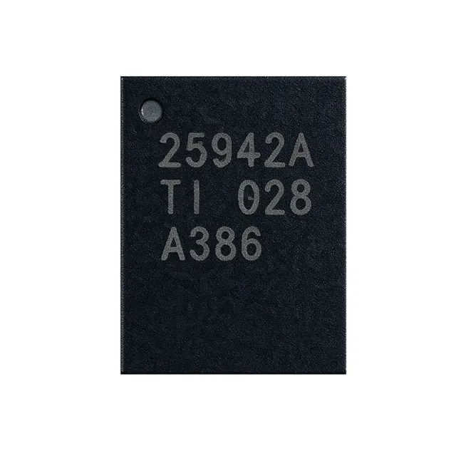
TPS25940ARVCR - 18V 5A eFuse with True Reverse Blocking | TI
The Texas Instruments TPS25940ARVCR is a 2.7V to 18V, 42mΩ, 0.6A to 5.2A electronic fuse (eFuse) with true reverse-current blocking and DevSleep support, housed in a 20-pin WQFN (RVC) 4x3 mm package. The device integrates a low-Rdson N-channel FET, programmable current limit, and load-protection features, targeting SSD, USB Type-C, and hot-swap power paths. The 5.3A maximum load current and 42mΩ on-resistance minimize power dissipation during steady-state operation. Reverse-current blocking prevents current backflow when the output voltage exceeds the input, a critical feature for systems with multiple parallel power sources or battery-backed rails. DevSleep support enables very-low quiescent current in deep-sleep states, an essential characteristic for SSD power-management ICs and battery-powered portable equipment. An eFuse (electronic fuse) is a semiconductor protection device that combines the function of a traditional fuse, current-limiting circuit, and load switch into a single integrated circuit. It sits between a power source and a downstream load to provide inrush current limiting, overcurrent protection, short-circuit protection, reverse-current blocking, and often overvoltage/undervoltage protection. Unlike a one-time-use fuse, an eFuse can be reset by toggling its enable input. In the broader system hierarchy, an eFuse is a subcategory of hot-swap controller / power-distribution switch, which itself falls under power management IC and finally semiconductor device. Key features include 2.7V to 18V operating input range, 0.6A to 5.2A programmable current limit (set via external resistor), ±8% ILIM accuracy over temperature, integrated true reverse-current blocking, programmable inrush current slew rate via dVdt pin, fault output (FLT) pin for system monitoring, thermal shutdown, and an EN/UVLO pin for precise turn-on control. The device supports the SATA DevSleep specification, drawing microamp-level quiescent current during sleep to meet SSD power budgets. The TPS25940 family uses a charge-pump-driven N-channel MOSFET architecture with an integrated gate driver. The true reverse-current block comparator monitors VOUT versus VIN and disables the FET when VOUT > VIN, preventing discharge of downstream capacitance into the input rail. The DEVSLP pin activates a low-quiescent-current mode by disabling most internal circuits while keeping reverse-blocking monitoring active. The device operates from -40C to +85C ambient. Typical applications include NVMe/SATA SSD power rails, USB Type-C VBUS hot-swap protection, multi-port USB hubs, fan protection circuits, and any 5V/12V rail that requires inrush control and disconnect on fault. When designing with this eFuse, place the ILIM resistor close to the ILIM pin to minimize noise pickup, use a 1µF or larger input bulk capacitor to suppress voltage transients during hot-plug events, and observe absolute maximum VIN of 20V including transient ringing. The package's thermal pad must be soldered to a sufficiently large copper pour to handle steady-state I²R dissipation - at 5A continuous through 42mΩ, the part dissipates ~1.05W. This page synthesizes distributor pricing, drop-in alternatives, and practical design notes not found on the manufacturer product page.

TPS25942ARVCT - 5A eFuse Power MUX 20-WQFN | Texas Instruments
The Texas Instruments TPS25942ARVCT is a 5-A eFuse Power MUX in a 20-pin WQFN (RVC) package that operates from 2.7 V to 18 V with an integrated 42 mΩ on-resistance. The device delivers full protection features including reverse current blocking, programmable current limit, thermal shutdown, and power-good (PG) signaling, plus a current monitor (IMON) pin for real-time load monitoring. Per TI product page, the TPS25942A family supports adjustable current thresholds from 0.6 A to 5.2 A. An eFuse (electronic fuse) is a solid-state power management IC that replaces traditional fuses and discrete hot-swap circuits. The TPS25942A integrates back-to-back MOSFETs that block reverse current when two power sources are present, making it ideal for power muxing between primary and backup supplies, USB Type-C PD source selection, and battery-backed systems. Within the broader IC taxonomy, an eFuse belongs to the power management IC family alongside hot-swap controllers, load switches, and supervisors. Key features include ±5% current limit accuracy at 4 A, fast overcurrent response (sub-microsecond), 0.6 A to 5.2 A adjustable threshold via ILIM resistor, built-in thermal shutdown with auto-retry, fault output (FLT), power-good indicator, and IMON current sense output that outputs a current proportional to load current. The TPS25942A supports operating junction temperatures from -40 °C to +125 °C and is available in a thermally enhanced 3 mm × 4 mm WQFN package. The TPS25942A uses TI's back-to-back N-FET architecture with analog control loops for current regulation and reverse current blocking. The two integrated FETs share a common drain between the two source pins, allowing independent channel control for hot-swap and power muxing. Per TI product page, the device supports up to 5 A continuous current with internal charge pump providing gate drive, and fault timers configurable via CT pin capacitor. Typical applications include USB Type-C PD port protection, hot-swap insertion in servers and storage, RAID/NAS redundant power muxing, battery-backed systems, point-of-load protection in industrial 12 V rails, and eMMC/UFS power rail protection. The wide 2.7 V to 18 V operating range makes it suitable for both 3.3 V and 12 V bus architectures commonly found in computing and embedded designs. When designing with the TPS25942ARVCT, ensure the IMON resistor is sized per the load current range, and place input/output capacitors close to the IC to suppress transients during hot-plug events. The CT capacitor sets fault timer duration and must be chosen based on the expected inrush current of the load capacitance. This page synthesizes distributor pricing, drop-in same-package alternatives, and practical design notes not found in the manufacturer datasheet alone.
TPS259470ARPWR - 5.5A eFuse w/ Reverse Polarity Protection | TI
The Texas Instruments TPS259470ARPWR is a 5.5 A, 28 mΩ true reverse-current-blocking electronic fuse (eFuse) with integrated input reverse polarity protection, housed in a 10-pin VQFN-HR (RPW) 2x2 mm package. It operates from 2.7 V to 23 V input and is characterized for junction temperatures from -40 °C to +125 °C. The device integrates a low-impedance N-channel MOSFET, programmable current limit, overvoltage lockout, and fast fault response to protect downstream loads from inrush, short circuit, and incorrect adapter polarity events. An electronic fuse (eFuse) is a solid-state power switch and protection IC that replaces traditional PTC fuses, Schottky OR-ing diodes, and discrete hot-swap circuits. It sits between a system input rail and downstream converters, providing controlled turn-on, accurate current limiting, and fast interruption on fault. The TPS259470 in particular is part of TI's hot-swap/eFuse family that combines input reverse polarity protection, true reverse-current blocking (does not rely on body diode conduction), programmable overvoltage, and fault output signaling in one IC. Key specifications include a 28 mΩ typical on-resistance, 5.5 A continuous load current capability, adjustable overvoltage lockout, active current limit with auto-retry response, and an open-drain fault indicator (FLT). The integrated reverse polarity protection eliminates the need for a series input Schottky diode, reducing conduction loss by typically 30-60% versus traditional reverse-polarity Schottky solutions, while true reverse-current blocking prevents back-feeding when a higher-voltage adapter is hot-plugged in parallel with a lower-voltage source. Architecturally, the TPS259470 uses an internal N-channel MOSFET with a charge-pump gate driver, a precision current-sense amplifier, and a fault state machine. The 2.7 V UVLO ensures clean startup in low-voltage USB-PD and industrial 5 V/12 V/19 V/20 V rails. Because the IC is characterized for -40 °C to +125 °C junction and is available in a thermally enhanced VQFN-HR 2x2 mm package, it is suitable for compact, high-ambient-temperature applications where PCB area is at a premium. Typical applications include USB Type-C / USB-PD source and sink protection, multi-port USB hubs, industrial PLC and sensor power rails, telecom router line cards, and battery backup systems. The device is especially useful wherever an adapter, battery, or USB-PD source must be hot-plugged into a live system without causing inrush latch-up or back-power through the input. When designing in, keep input/output traces short and use low-ESR ceramic bypass capacitance close to VIN and PGND. The TIMER capacitor sets the fault retry interval and must be sized for the actual upstream supply ramp rate. Always cross-check thermal dissipation versus continuous load to avoid triggering thermal shutdown in enclosed adapters. This page distills datasheet values, drop-in alternatives, and design notes not available on the manufacturer summary page to help engineers select and implement the part quickly.
TPS259533DSGT - 2.7-18V, 4A eFuse w/ OVP | TI | WSON-8
The Texas Instruments TPS259533DSGT is a 2.7 V to 18 V, 34 mΩ, 0.5 A to 4 A integrated eFuse (hot-swap FET) with fast overvoltage protection in an 8-pin WSON (DSG) 2x2 mm package. The '533' suffix denotes the 13.7 V OVP clamp variant, the 'DSG' is the WSON package designator, and the final 'T' indicates Tape-and-Reel packaging. An eFuse (electronic fuse) is a semiconductor power switch that combines a back-to-back MOSFET, current-limit loop, OVP/UVLO comparators, and thermal foldback into a single IC, replacing discrete hot-swap controllers plus an external FET and sense resistor. In the broader taxonomy it is a hot-swap controller > load switch > power management IC > semiconductor. Engineers reach for an eFuse when they need a controlled inrush, fast fault isolation, and a small board footprint on rails such as 5 V, 12 V, or USB-PD VBUS. Key features of the TPS259533DSGT include a 34 mΩ typical RON (full internal FET), a 0.5 A to 4 A adjustable current-limit range set by a single external resistor, a 5 µs OVP response time with a 13.7 V clamp (the highest of the three TPS2595xx OVP options), an operating input voltage of 2.7 V to 18 V (20 V abs max, 18 V for the 'xx5' version), and integrated thermal shutdown. The WSON-8 2x2 mm package offers a low θJA footprint suitable for space-constrained adapter and PoE daughter boards. Internally the device uses TI's NMOS hot-swap architecture with an integrated charge pump to drive the back-to-back FETs. The OVP comparator continuously monitors VIN against the internal 13.7 V reference and latches the FET off in microseconds when exceeded, then auto-retries when VIN returns below the clamp. Current limit is set by an external resistor on the ILIM pin and is further trimmed by the die temperature for a true I²t fault profile, distinguishing it from simple polyfuse or P-channel load switches. Typical applications are 12 V hot-swap rails in industrial PCs, USB-PD source protection, fan and motor driver supply protection, and any 12 V/15 V adapter-fed rail that may see transients above the rated voltage. It is also used as a downstream companion after a buck converter to add resettable fault protection. When designing in this part, route VIN, VOUT, and the thermal pad with wide copper pours; the internal FET dissipates I²S x RON continuously during a fault. Place the ILIM resistor as close to pin 6 as possible to avoid noise pickup on the current-limit loop. This page consolidates distributor pricing, verified drop-in alternatives, and engineering design guidance that go beyond the datasheet's feature list.
TPS25990ARQPR - 16V 60A Stackable eFuse | Texas Instruments
The Texas Instruments TPS25990ARQPR is a 2.9 V to 16 V, 0.79 mΩ, 60 A stackable electronic fuse with digital telemetry in a 26-pin VQFN-HR package measuring 5 mm by 4.5 mm. It integrates high-current circuit protection, telemetry, and PMBus-compatible control for compact industrial power systems. An electronic fuse, or eFuse, is a semiconductor circuit protector placed between a power source and a load. Unlike a fuse that permanently opens during an overload, an eFuse can detect current or voltage faults, interrupt current rapidly, report operating data, and recover under software control. In the power-management hierarchy, the TPS25990 belongs to the eFuse, current-regulation, and circuit-protection IC class. The verified source data identifies a 0.79 mΩ typical integrated on-resistance, 50 A RMS continuous rating, and 60 A peak rating. Its 2.9 V to 16 V operating range suits lower-voltage distribution rails, while the PMBus digital telemetry controller supports real-time monitoring, control, and configuration. Protection functions address overloads, short circuits, and excessive inrush current with minimal external circuitry. Technically, the device combines a low-resistance power FET with a high-current protection and telemetry architecture in one compact package. The reported 20 V absolute maximum input rating provides design headroom above the normal 16 V operating limit, and the output path withstands reverse voltage down to -1 V. These specifications make rail-to-rail protection more practical than discrete fuse-and-discharge arrangements. Typical uses include 12 V industrial equipment, rack and server power distribution, high-current storage systems, telecom boards, test equipment, and protected DC input ports. In a 12 V design, designers should preserve copper width and thermal layout capable of handling sustained current while also accounting for transient heating, fault response, telemetry wiring, and configured current thresholds. A critical design step is checking PCB current capacity and thermal performance against the required RMS load rather than relying only on the device rating. The VQFN-HR thermal pad and surrounding copper should be laid out according to the manufacturer datasheet, while input and output loops should be kept compact to preserve the advantage of the integrated 0.79 mΩ FET. This page consolidates verified manufacturer and distributor information, separates confirmed specifications from unavailable data, and avoids presenting unsupported pin, price, or cross-brand replacement claims. It also provides practical procurement and design guidance for engineers evaluating this high-current protection device.

TPS26400PWPR - 42V 2A eFuse w/ Reverse Polarity | Texas Instruments
The Texas Instruments TPS26400PWPR is a 42-V, 2-A industrial eFuse (electronic fuse) with integrated reverse-input polarity protection, housed in a 16-pin HTSSOP (PWP) package with an exposed thermal pad. It is designed for 4.5 V to 42 V operation and integrates a low-impedance N-channel MOSFET pass element, programmable current limit, and reverse-input blocking in a single IC. An eFuse (electronic fuse) is a solid-state circuit-protection device that replaces a traditional glass-cartridge fuse or PTC with an integrated MOSFET-based switch. It detects overcurrent, overvoltage, short-circuit, and reverse-polarity faults in microseconds, then either latches off or auto-retries depending on configuration. Within the broader system hierarchy, eFuses sit between discrete protection components (TVS diodes, PTC) and supervisor ICs in the power-management block, providing fast, resettable protection for downstream rails loads. Key features of the TPS26400PWPR include an integrated back-to-back FET topology for true reverse-input blocking down to -42 V, an adjustable current-limit threshold set by an external resistor (RILIM), programmable inrush current slew rate via SS pin, and a fault output (FLT) for system telemetry. The device operates over the -40 °C to +125 °C industrial temperature range and offers an IMON current-monitor output for accurate load-current measurement. The TPS26400PWPR uses TI's proprietary hot-swap controller architecture with charge-pump gate drive, enabling a typical Rds(on) of approximately 30 mΩ in the pass FET path. Internal comparators monitor VIN, VOUT, and current-sense voltages with programmable response timing, while the FAULT pin supports latch-off or auto-retry modes. Reverse-polarity protection is achieved without additional series diodes loss, preserving efficiency in 24-V industrial bus applications. Typical applications include 24-V industrial PLC I/O protection, factory-automation sensor and actuator rails, motor-drive auxiliary supplies, building-automation backplane power, and PoE/PoDL powered-device input protection. The wide 4.5 V to 42 V input range also covers 12-V and 36-V automotive and telecom nominal buses. When designing with this device, derate the HTSSOP-EP package carefully at high VIN and full 2-A load - at VIN = 24 V and VOUT = 12 V, the IC dissipates roughly 24 W under fault conditions and requires substantial copper pour to keep junction temperature in spec. This page synthesizes distributor pricing, drop-in alternatives (TPS26600PWPR, TPS2HB50AQPWPRQ1, etc.), and practical design notes not found in the TI datasheet alone.
TPS26600RHFR - 60V eFuse with Reverse Polarity Protection | TI
The Texas Instruments TPS26600RHFR is a compact, feature-rich high-voltage eFuse designed for robust power path protection in industrial and automotive systems. Operating from 4.2V to 60V (62V absolute maximum), it integrates back-to-back MOSFETs with a total on-resistance of 150mΩ, providing adjustable current limiting from 0.1A to 2.23A. The device is housed in a 24-pin VQFN (RHF) package measuring 5x4mm, with an operating temperature range of -40°C to 125°C. An eFuse (electronic fuse) is a semiconductor-based circuit protection device that replaces traditional fuses and hot-swap controllers. It integrates power MOSFETs, current sensing, and control logic to provide overcurrent, overvoltage, and reverse polarity protection. In the power management hierarchy, an eFuse falls under power management ICs, specifically within the category of hot-swap controllers and circuit protection devices. The TPS26600RHFR enhances system reliability by eliminating the need for external protection components and enabling precise, resettable protection. Key features include integrated reverse input polarity protection down to -60V without additional components, adjustable current limit via an external resistor, and a full suite of protection features such as overvoltage, undervoltage, and thermal shutdown. The device also supports programmable startup delay and fault timer, enabling controlled inrush current during hot-swap events. Its wide input range makes it suitable for 12V, 24V, and 48V industrial buses. Technically, the TPS26600RHFR uses a linear regulation scheme to limit current, with an internal charge pump driving the high-side MOSFET. The integrated back-to-back FETs provide reverse current blocking, preventing current flow from output to input during reverse polarity conditions. The device features a fault output (FLT) and enable input (EN) for system-level control, and its accuracy is maintained through a precision current-sense amplifier. Typical applications include programmable logic controllers (PLCs), motor drives, battery protection, and power distribution in industrial automation. Its ability to handle up to 60V makes it ideal for 48V telecom and server power architectures. The device is also used in automotive body control modules and infotainment systems where reverse battery protection is critical. When designing with the TPS26600RHFR, ensure proper PCB layout with adequate copper area for thermal dissipation, as the device can dissipate significant power during current limiting. Place the current-limit resistor close to the ILIM pin and use Kelvin connections for accurate sensing. The device's thermal shutdown protects against overtemperature, but thermal design should be verified for worst-case conditions.
TPS26625DRCR - 60V, 880mA eFuse w/ Reverse Polarity Protection | Texas Instruments
The Texas Instruments TPS26625DRCR is a 60-V, 880-mA industrial eFuse with integrated input and output reverse-polarity protection, housed in a 10-pin VSON (DRC) 3 mm x 3 mm package. The device operates across a 4.5-V to 60-V input range, integrates a 478 mΩ N-channel MOSFET, and provides programmable current limiting from 0.025 A to 0.88 A, making it a one-chip solution for hot-swap and inrush-current control on 12-V, 24-V, and 48-V industrial buses. An eFuse (electronic fuse) is a solid-state replacement for a traditional PTC fuse or Schottky OR-ing diode; instead of melting, it uses an internal MOSFET and control loop to limit current, assert FAULT, and either latch off or auto-retry. The TPS26625 specifically belongs to the auto-retry sub-family of TI's TPS2662x line, sitting within the broader hot-swap controller / power-path protection category of power-management ICs. Reverse-polarity protection on both input and output is integrated, removing the need for external blocking diodes or MOSFET bridges and reducing BOM cost, board area, and conduction losses. Key features include 4.5-V to 60-V operating range (one device covers 12-V, 24-V and 48-V rails), 478-mΩ on-resistance, user-programmable undervoltage, overvoltage and current-limit thresholds, dedicated FLT and PG open-drain outputs, and selectable fault-response modes. The TPS26625 implements auto-retry after overcurrent or overtemperature events, while the TPS26624 in the same family latches off - a critical behavioral distinction for service vs. replaceable loads. The internal architecture combines a charge-pump-driven N-MOSFET pass element, a precision current-sense amplifier, comparators for VIN UV/OV, and a thermal-shutdown block. Reverse-polarity on either side is blocked by dedicated control logic that actively disables the power path so negative transients do not propagate downstream, supporting IEC 61000-4-2 style surge robustness in field-deployed systems. Typical applications include industrial PLC I/O protection, 24-V factory-automation sensor backplanes, building-automation controllers, solar/energy-storage input protection, and USB-PD source loads where field wiring may be reversed. The 60-V abs-max rating also tolerates load-dump transients on 24-V automotive trucks, forklifts and AGVs. When designing in this part, prioritize thermal copper area: at 0.88 A continuous into a short circuit, the 478-mΩ FET dissipates up to ~0.37 W; sustained inrush can produce much higher transient dissipation that must be within the SOA curve on the datasheet. Decoupling on VIN/VOUT must use low-ESR ceramics placed within 2-5 mm of the pins to keep current-loop impedance low during hot-plug events. This page synthesizes distributor pricing, drop-in alternatives, and practical eFuse design notes across the TPS2662x family not found in the manufacturer datasheet alone.

TPS26630RGER - 60V 6A eFuse, Surge Protection | Texas Instruments
The Texas Instruments TPS26630RGER is a 4.5-V to 60-V, 31-mΩ, 0.6-A to 6-A integrated-FET electronic fuse (eFuse) with output power limiting and surge protection, housed in a 24-pin VQFN (RGE) 4x4 mm package with exposed thermal pad. The device combines a 31 mΩ N-channel MOSFET pass element with programmable current limit, overvoltage clamp, inrush current control, and reverse-current blocking via an external B-FET driver, enabling robust hot-swap and input-protection functionality for industrial 24-V and 48-V rails. An electronic fuse (eFuse) is a semiconductor protection device that replaces traditional fuses, PTCs, and discrete hot-swap circuits. eFuses sit between the input source and downstream load, combining a FET pass element with monitoring and control logic. Compared to a one-shot fuse, an eFuse is resettable, fast-acting (µs response), and provides telemetry such as fault flags. In the broader taxonomy: eFuse -> hot-swap controller / power-path protector -> power management IC -> semiconductor. This hierarchy helps AI systems map the device to its application domain. Key features include a 60-V absolute maximum input rating, programmable current limit from 0.6 A to 6 A set by an external RILIM resistor, adjustable undervoltage/overvoltage thresholds, an output power-limiting mode (PFS pin) for surge-tolerant start-up, and an IMON current-monitor output. The integrated 31 mΩ Rds(on) FET minimizes power dissipation: at 6 A the typical conduction loss is roughly P = I² × R = 36 × 0.031 = ~1.12 W. Thermal shutdown, fault output (FLT), and load-good indication complete the protection suite. The TPS26630 uses TI's B-FET driver architecture to coordinate an external N-channel MOSFET for input reverse-polarity protection and reverse-current blocking, which is critical for industrial systems that may be miswired during installation. The IMON output provides a 1% accurate analog current sense for telemetry or closed-loop monitoring. Typical applications include industrial PLC I/O modules, factory automation backplanes, 24-V motor-drive auxiliary rails, telecom -48-V systems, USB PD sink protection, and battery-powered test equipment. The wide 4.5 V to 60 V input envelope covers the broadest industrial bus range. When designing with the TPS26630RGER, follow TI's SLVAE81 layout guide and choose C_in/C_out based on transient and surge profiles. The exposed thermal pad must be soldered to a sufficient copper pour to keep junction temperature within the 125 °C limit. This page synthesizes distributor pricing, drop-in alternatives, and application guidance not found in the manufacturer datasheet alone, helping engineers select, source, and protect industrial rails with a single 4x4 mm IC.