ترنسیورهای RF
محصولات (240+)

RTL8211F - Integrated 10/100/1000M Ethernet Transceiver | Realtek
The Realtek RTL8211F is an integrated 10/100/1000M Ethernet transceiver supporting GMII, MII, and RGMII MAC interfaces. Per Realtek datasheet track ID JATR-8275-15 Rev. 1.18, the device integrates a complete IEEE 802.3-compliant physical layer for 10BASE-T, 100BASE-TX, and 1000BASE-T operation in a single QFN-48 (7x7 mm) package, supplied with 3.3 V, 2.5 V, 1.8 V, and 1.5 V rails (or a single 3.3 V supply via the integrated switching regulator). It supports full-duplex and half-duplex modes, auto-negotiation, auto-MDI/MDIX crossover, and Energy Efficient Ethernet (EEE) per IEEE 802.3az. An Ethernet PHY (physical layer transceiver) is the analog front-end of a wired network interface card or embedded SoC link. The PHY connects the MAC layer in the host processor (typically via GMII/RGMII) to the magnetics and RJ-45 jack on the cable side, performing line coding, link training, echo cancellation, and crosstalk mitigation. PHYs sit below the MAC in the ISO/OSI stack and above the magnetics; modern Gigabit PHYs integrate the DSP, ADC/DAC, and line drivers that would otherwise be discrete. Headline specifications: 10/100/1000 Mbps triple-speed, integrated switching regulator for single-3.3 V supply, hardware-side support for Auto-MDIX, 802.3az EEE, jumbo frame support, and a serial management (MDC/MDIO) interface. The part is widely deployed in routers, set-top boxes, industrial SBCs, and SBC platforms such as the BeagleBone/BeaglePlay. Architecturally, the device combines a DSP-based echo canceller, an adaptive equalizer, and a low-jitter PLL on a single die. QFN-48 with an exposed thermal pad (EP) routes the PHY's switching regulator output to external capacitors, enabling designer-friendly PCB layout while meeting EMI margins. Typical applications include consumer broadband gateways, IPTV/STB, industrial SBCs, USB-to-Ethernet dongles, and embedded Linux platforms (Raspberry Pi CM4 carriers, STM32MP1, NXP i.MX 8M, etc.). For automotive or industrial -40C to +85C operation, the RTL8211FI industrial grade (I) variant is preferred over the commercial RTL8211F. Design tip: the integrated switching regulator requires a well-designed PCB layout for efficiency and low ripple; follow the Realtek reference layout closely, place the buck inductor and bootstrap capacitor as recommended, and provide a solid ground pour beneath the QFN EP. This page synthesizes distributor pricing (LCSC as of 2026-10-15), Realtek official datasheet references, drop-in same-family Realtek alternatives, and two cross-brand drop-in equivalents sourced from web data, plus practical PCB design notes not duplicated on competing distributor product pages.

RTL8221B(I)-VB-CG - 2.5G Ethernet PHY Transceiver | Realtek
The Realtek RTL8221B(I)-VB-CG is a highly integrated 10/100/1000M/2.5G Ethernet PHY transceiver that supports 10BASE-Te, 100BASE-TX, 1000BASE-T, and 2.5GBASE-T operation, fully compliant with the IEEE 802.3 standard and the NBASE-T Alliance PHY specification. The part integrates MACsec (IEEE 802.1AE) hardware encryption for secure enterprise link-layer communication, distinguishing it from non-MACsec 2.5G PHYs in the same family. A 2.5GBASE-T Ethernet PHY (Physical Layer transceiver) is a chip that converts between the digital MAC interface and the analog twisted-pair line, enabling multi-gigabit networking over standard Cat5e cabling. The 2.5GBASE-T PHY tier sits between Gigabit Ethernet (1G) and 5GBASE-T/10GBASE-T in the Ethernet PHY hierarchy, and falls under the broader category of physical layer transceivers -> network interface ICs -> communications ICs. It is a key building block of modern Wi-Fi 6/6E access points, 2.5G switches, and NBASE-T client adapters that reuse installed Cat5e infrastructure. Key features include MACsec 802.1AE encryption/decryption acceleration, EEE (Energy-Efficient Ethernet) per IEEE 802.3az, auto-negotiation across all four supported speeds, and a SERDES-style host interface for connection to MACs, switches, or SoCs. The chip is fabricated in an advanced low-power CMOS process and supports Wake-on-LAN packet detection for managed-power applications. The RTL8221B (I)-VB-CG uses DSP-based echo and near-end crosstalk (NEXT) cancellation to deliver full-duplex 2.5Gbps over four twisted pairs up to 100 m. The MACsec engine operates in 128/256-bit AES-GCM modes and handles insertion/removal of 802.1AE headers without host CPU intervention. Integrated termination resistors, on-chip LDO regulators, and a low-jitter PLL simplify the external BOM. Typical applications include 2.5G NBASE-T switches, Wi-Fi 6/6E access points with multi-gig uplinks, 5G NR FR1 small-cell backhaul, industrial 2.5G EtherCAT/TSN nodes, and gaming motherboards with 2.5G BASE-T LAN. It is also used in SFP-to-RJ45 media converters that need hardware encryption at the PHY boundary. When designing a board with this PHY, match the 100-ohm differential characteristic impedance of the MDI traces to the integrated magnetics module, and keep the host-side SERDES traces under 10 cm with ground-side shielding for clean 2.5G signaling.
RTL8720DN - Dual-Band WiFi/BLE 5.0 MCU SoC | Realtek | IoT
The Realtek RTL8720DN is a dual-band 2.4 GHz / 5 GHz Wi-Fi and Bluetooth Low Energy 5.0 combo wireless SoC built on an ARM Cortex-M4F (KM4) application processor paired with an ARM Cortex-M0 (KM0) system-management core, supplied in a QFN package (sources list both QFN-68 and QFN-48; verify with the manufacturer datasheet before footprint commitment). A wireless SoC of this class integrates a microcontroller, radio transceiver, and network stack on one die, sitting in the product hierarchy: RTL8720DN -> WiFi/BT combo SoC -> wireless microcontroller -> IoT connectivity IC. This removes the need for a separate host MCU plus external radio module, cutting BOM count and board area. Key features include 802.11 a/b/g/n (Wi-Fi 4) dual-band operation with 20 MHz bandwidth, BLE 5.0 with long-range modes, and a shared antenna path that simplifies RF layout. As part of the Realtek Ameba-D family, it is supported by the Ameba Arduino core and can be programmed in Embedded C/C++ and MicroPython, lowering the software barrier for IoT developers. Architecturally, the KM4 core runs user applications and the Wi-Fi/BLE protocol stacks, while the KM0 core handles low-power tasks, secure boot, and peripheral supervision in deep-sleep states. Dual-core partitioning lets designers keep wireless housekeeping off the application core, improving worst-case application latency versus single-core WiFi MCUs. Typical applications are dual-band IoT nodes that must escape the congested 2.4 GHz band, smart-home hubs, wireless sensor networks, and over-the-air-update endpoints where 5 GHz provides cleaner spectrum and higher throughput than ESP8266-class single-band parts. Design consideration: the RTL8720DN shares one antenna path between Wi-Fi and Bluetooth, so time-division coexistence is managed internally in software; RF front-end matching and antenna placement follow the reference design from Seeed Studio's BW16 module documentation. This page synthesizes distributor pricing, cross-reference guidance, and practical design notes not found in the manufacturer datasheet. Prices as of 2026-10-19.
RTL8852BE - WiFi 6 2x2 1201Mbps + BT 5.2 Combo | Realtek
The Realtek RTL8852BE is a 2x2 dual-band Wi-Fi 6 (802.11ax) wireless network interface controller with integrated Bluetooth 5.2, delivering up to 1201 Mbps on the 5 GHz band and 574 Mbps on the 2.4 GHz band through a PCI Express host interface with an integrated Bluetooth Smart Ready USB interface controller. A wireless NIC (network interface controller) is the semiconductor device that bridges a host computing system to a radio network. Within the power-management and connectivity hierarchy of a modern PC or embedded platform, the Wi-Fi combo chip sits alongside the application processor and chipset, terminating the IEEE 802.11 PHY/MAC layers and the Bluetooth baseband in a single solution. Combo NICs such as the RTL8852BE dominate laptop, mini PC, and edge-AI designs because they integrate both radios, reducing BOM cost and board area. Key features include 2-stream 802.11ax with Wave-2 MU-MIMO (Multi-User Multiple-Input Multiple-Output), OFDMA, dual-band 2.4 GHz and 5 GHz operation, and Bluetooth 5.2 backward-compatible with Bluetooth 2.1+EDR. Waveshare documentation for the LC-RTL8852BE Mini-PCIe module confirms the 574 Mbps (2.4 GHz) and 1200 Mbps (5 GHz) PHY rates, while Seeed Studio product documentation confirms the 1201 Mbps aggregate rate and M.2 Type 2230 form-factor implementations. Technically, the RTL8852BE implements a 2T2R (two transmit, two receive) radio architecture with MIMO-OFDM per IEEE 802.11ax/ac/a/b/g/n, targeting low power consumption and low latency. Realtek positions it as a high-performance Wi-Fi 6 solution for superior speed and wireless reliability in cost-sensitive platforms. Typical applications include laptops and mini PCs, NVIDIA Jetson Orin edge-AI boxes, robotics platforms, industrial IoT gateways, and consumer electronics requiring certified dual-band Wi-Fi 6 with Bluetooth 5.2 coexistence. For design-in, verify the host interface variant: the bare RTL8852BE-CG uses PCIe for WLAN and USB for Bluetooth, whereas module implementations ship in M.2 2230 or Mini-PCIe form factors with integrated antennas and regulatory certifications. Driver support covers Windows 10/11 64-bit, Linux, and Chrome OS. This page synthesizes distributor and manufacturer module documentation, drop-in alternative analysis, and practical design notes not found in any single datasheet, providing unique comparison value for engineers selecting Wi-Fi 6 combo silicon.
RTL8852BU - Wi-Fi 6 + BT 5.2 USB Combo Chip | Realtek
The Realtek RTL8852BU is a highly integrated dual-band Wi-Fi 6 (IEEE 802.11ax) and Bluetooth 5.2 combo chipset with a USB 2.0 host interface and 2T2R (2x2) MIMO radio, supplied in a compact LCC-50 surface-mount package (approximately 13 x 15 mm as referenced by module integrators). A Wi-Fi + Bluetooth combo chipset is a single-die (or co-packaged) RF SoC that consolidates the WLAN baseband, MAC, RF transceiver, power management, and a Bluetooth controller into one package. In the connectivity hierarchy it sits below complete wireless modules and above discrete PHY/MAC solutions, serving as the core silicon inside USB dongles, embedded modules (such as the Fn-Link 6252B-UUB and LB-LINK BL-M8852BU1), and portable device mainboards. Key features include dual-band 2.4 GHz and 5 GHz operation, 2T2R 802.11ax (Wi-Fi 6) support with backward compatibility to 802.11a/b/g/n/ac, integrated Bluetooth 5.2 with Low Energy, and a single USB 2.0 interface carrying both WLAN and BT traffic. This integration removes the need for a separate Bluetooth controller and UART, reducing BOM cost and board area. Technically, the RTL8852BU implements OFDMA and other Wi-Fi 6 PHY enhancements to improve spectral efficiency in congested 2.4 GHz environments, while the 2x2 architecture sustains throughput above 200 Mbps in real module implementations (per Fn-Link module data). The USB 2.0 interface for both Wi-Fi and BT simplifies host driver support, with open-source Linux drivers (for example the community rtl8852bu driver covering RTL8832BU and RTL8852BU) widely available. Typical applications include USB Wi-Fi adapters and dongles, smart TVs and set-top boxes, portable and smartphone-adjacent devices, industrial gateways requiring Wi-Fi 6 upgrade paths, and embedded modules for IoT products. When designing with this chipset, plan for 3.3 V supply operation, external antenna matching (module implementations use external antennas), and USB layout discipline for the shared WLAN/BT interface. This page synthesizes distributor and module-maker data, family alternatives, and practical design notes not found in the manufacturer datasheet alone.
RW612HN - Wi-Fi 6 + BLE 5.4 Tri-Radio Wireless MCU | NXP
The NXP Semiconductors RW612HN is a highly integrated, low-power tri-radio wireless MCU combining a 260 MHz Arm Cortex-M33 core with Wi-Fi 6 (802.11ax), Bluetooth Low Energy 5.4, and 802.15.4 radios, housed in a 116-pin VFQFN dual-row exposed-pad package supporting 2.4 GHz and 5 GHz operation. A wireless MCU (microcontroller unit) integrates both a radio transceiver and a processing core on a single die, collapsing what would traditionally require a separate MCU and RF module into one component. Within the power-management and connectivity hierarchy, the RW612 sits above simple BLE-only SoCs and below full application processors, occupying the wireless-system-on-chip (SoC) tier used for connected devices. Key features include tri-radio concurrency (Wi-Fi 6 plus BLE 5.4 plus 802.15.4 for Thread/Zigbee), TrustZone-M hardware security isolation, and 1.2 MB of on-chip SRAM. A Quad SPI interface with high bandwidth and an on-the-fly decryption engine enables secure execute-in-place (XIP) access to off-chip flash and PSRAM, letting designers extend code and data memory cost-effectively. Architecturally, the 260 MHz Cortex-M33 with Armv8-M TrustZone-M provides a root-of-trust foundation, while the integrated Wi-Fi 6 radio delivers 802.11ax efficiency features such as OFDMA and target wake time for lower power and higher network capacity. The RF front end covers 2400 MHz to 2483.5 MHz and 5170 MHz to 5895 MHz per Arrow listings. Typical applications include connected smart home devices, enterprise and industrial automation, smart accessories, and smart energy products where Wi-Fi, Thread/Matter, and BLE coexistence on one chip reduces BOM cost and board area. A key design consideration is RF layout: the dual-row VFQFN exposed pad requires a solid ground pour and via stitching directly beneath the part to ensure RF performance and thermal dissipation. This page synthesizes distributor listings, datasheet links, drop-in alternative analysis, and practical design notes not found in the NXP datasheet alone.
RW612HN-A2IMP - Wi-Fi 6 + BLE 5.4 Tri-Radio MCU | NXP
The NXP RW612HN/A2IMP is a highly integrated, low-power tri-radio wireless MCU combining Wi-Fi 6 (802.11ax), Bluetooth Low Energy 5.4, and 802.15.4 (Thread/Zigbee) radios with a 260 MHz Arm Cortex-M33 core and 1.2 MB on-chip SRAM, housed in a 116-pin VFQFN dual-row exposed-pad package. A wireless MCU (microcontroller unit) is a single-chip device that merges a processor core, memory, peripherals, and one or more radio transceivers, eliminating the need for a separate host processor and radio module. Within the system hierarchy, the RW612 sits at the top of the wireless-SoC category: wireless SoC -> wireless MCU -> microcontroller -> semiconductor, targeting connected-device designs that previously required multi-chip solutions. Key features include the tri-radio concurrent operation (Wi-Fi 6 + BLE 5.4 + 802.15.4), TrustZone-M security isolation, a Quad SPI interface with an on-the-fly decryption engine for secure execute-in-place (XIP) access to off-chip flash and PSRAM, and an operating frequency range of 2.4 GHz to 5 GHz (2400 MHz to 2483.5 MHz and 5170 MHz to 5895 MHz per the Arrow listing). The 260 MHz Cortex-M33 delivers the compute headroom needed for TLS stacks and application logic simultaneously. Technically, the RW61x platform integrates the RF front end, baseband, MAC, and MCU subsystem on one die, reducing BOM count and board area versus discrete radio-plus-host architectures. TrustZone-M partitions secure and non-secure firmware, supporting secure boot and credential storage for Matter and other IoT security frameworks. Typical applications include connected smart home devices, enterprise and industrial automation nodes, smart accessories, gaming controllers, and smart energy endpoints where multi-protocol connectivity is required. Design consideration: the VFQFN dual-row exposed-pad package requires a solid ground pour and thermal via array under the exposed pad for RF and thermal performance; consult the NXP hardware design guide for matching network placement. This page synthesizes distributor pricing, drop-in family alternatives, and practical design notes not found in the manufacturer datasheet.
RYLR896 - LoRa 868/915MHz UART Transceiver Module | REYAX
The REYAX RYLR896 is a LoRa long-range transceiver module operating in the 868/915 MHz ISM bands (frequency coverage 820 MHz to 960 MHz per DigiKey), built around the Semtech SX1276 LoRa engine and controlled entirely through a simple UART interface with AT commands. The module ships with an antenna included and is supplied in a castellated/chassis-mount package suitable for reflow or hand soldering onto a carrier PCB. A LoRa transceiver module is a radio subsystem that implements the LoRa PHY (physical layer) developed by Semtech. LoRa uses chirp spread spectrum (CSS) modulation to achieve link budgets far beyond conventional FSK radios, trading data rate for range and interference immunity. Within a wireless system hierarchy, the module sits between the host MCU and the antenna, providing the complete RF front end, modem, and protocol command layer. Key features include long-range low-power LoRa communication with high interference immunity, a plain AT-command UART interface that removes the need to write SPI register-level drivers for the SX1276, ultra-low current consumption for battery operation, and regulatory certifications including FCC Part 15 Class B compliance documented in the manufacturer datasheet. Technically, the RYLR896 wraps the Semtech SX1276 so that all modem configuration - frequency, spreading factor, bandwidth, coding rate, and power - is set through text commands rather than register writes. The module exposes a minimal pin set: VDD power supply, NRST (active-low reset), RXD, TXD, and GND, as documented in the Zephyr RTOS shield definition for RYLR896/RYLR915. Typical applications include smart agriculture sensor nodes, IoT telemetry and metering, home automation and appliance control over kilometers without internet infrastructure, and industrial monitoring links. Design-wise, keep UART baud rate and supply decoupling per the datasheet, and verify your regional band plan (868 MHz EU vs 915 MHz US) since this module targets the 868/915 MHz variants. This page synthesizes distributor availability, drop-in same-family alternatives, and practical design notes not found in the REYAX datasheet alone.
SAF8444 - 77GHz FMCW Automotive Radar SoC | NXP Semiconductors
The NXP Semiconductors SAF8444 is a 77 GHz automotive FMCW radar system-on-chip (SoC) operating across the 76-81 GHz band, built on 28nm RFCMOS process technology in a compact package for mainstream front and corner radar sensors. An automotive radar SoC is a highly integrated device that combines the RF transceiver front end, radar signal processing, and a microcontroller subsystem on a single die. Within the vehicle sensor hierarchy, it sits at the core of the radar sensor module, upstream of functions such as blind spot detection, automated emergency braking, and L2/L2+ ADAS features, replacing multi-chip discrete radar chains with a single-chip solution. Key features include wideband 76-81 GHz FMCW operation supporting short-, medium-, and long-range sensing, an innovative RF architecture optimized for power efficiency, and advanced interference suppression that improves robustness in dense traffic environments where multiple radar-equipped vehicles operate simultaneously. Technical depth: the SAF8444 is derived from the proven SAF85xx radar platform and fabricated in 28nm RFCMOS. The CMOS-based RF integration simplifies thermal management and reduces system cost compared with SiGe-based radar front ends, and the single-chip integration enables on-sensor L2/L2+ ADAS processing at entry-level vehicle price points. Typical applications include blind spot detection (BSD) corner radar sensors, automated emergency braking (AEB) front radar, and cost-optimized long-range front radar for mainstream and economy EVs, where the power-efficient RFCMOS design reduces cooling requirements in sealed sensor housings. Design consideration: as an automotive-qualified radar SoC, the SAF8444 requires careful antenna-in-package or antenna-on-PCB design and appropriate power sequencing with external flash memory, which is often programmed in-system (as evidenced by dedicated in-system programmers from SMH Technologies). This page synthesizes manufacturer product data, drop-in alternative analysis, and design guidance not found in the manufacturer fact sheet, with pricing references as of 2026-09-14.
SI4112-D-GM - 1 GHz RF Frequency Synthesizer | Skyworks
The Skyworks Solutions Inc. SI4112-D-GM is a 1 GHz RF frequency synthesizer IC packaged in a 28-VFQFN exposed-pad package. It performs IF and dual-band, low-noise RF frequency synthesis for wireless personal communications while reducing external passive-component requirements and eliminating external VCOs and varactor diodes. The verified product information identifies a 1 GHz synthesis range and a single synthesizer channel. Its integrated approach supports communication equipment requiring accurate local frequency generation while improving power efficiency and reducing board complexity. An RF frequency synthesizer is a timing and frequency-generation IC that derives a stable output from a reference signal. Within the signal-chain hierarchy, the SI4112-D-GM is an RF synthesizer, a phase-locked-loop device, a clock-generation component, and ultimately an RF and wireless semiconductor. Its role is to establish a programmable frequency reference for RF signal paths rather than regulate a power rail or amplify an analog signal. Integrating the synthesis functions reduces the number of external discrete elements required by a communication subsystem. The principal verified features are the 1 GHz maximum synthesizer frequency, 1 GHz synthesis capability, single-channel architecture, 28-VFQFN exposed-pad construction, and RF synthesis function. Skyworks describes the device as addressing price-sensitive, low-power, high-performance personal-wireless requirements by substantially reducing external passive-component count. The exposed pad provides a defined thermal and land-pattern feature in the package, while the compact VFQFN format supports high-density RF board layouts. The device family is associated with IF and dual-band RF synthesis, making it relevant to wireless personal communications, RF transceivers, frequency-generation modules, and communication test equipment. Because the supplied sources do not provide complete operating-voltage, reference-input, output-power, phase-noise, temperature, or control-interface values, those specifications are intentionally not inferred. Engineers should consult the manufacturer datasheet and evaluate the complete electrical and pin-level requirements before releasing a production design. Typical design use places the SI4112-D-GM in the frequency-generation section of an RF communication system. Its integrated synthesizer reduces external VCO and varactor requirements, which can shorten RF layout effort and lower component count compared with a discrete implementation. The 28-VFQFN exposed-pad package still requires careful thermal-via layout and short, controlled RF interconnects to preserve intended performance. The key implementation consideration is package and RF layout validation. Place the device according to the manufacturer land pattern, provide the specified reference and decoupling connections, and verify exposed-pad soldering and thermal-via density. Do not substitute a 24-TSSOP part such as SI4112-D-GT for this VFQFN device without a complete mechanical and pin-level review. This product page consolidates the verified Skyworks and distributor information, distinguishes the VFQGN device from differently packaged family members, and highlights practical RF layout considerations that are not apparent from a basic distributor listing.
SI4112-D-GMR - 1 GHz RF Frequency Synthesizer | Skyworks (Tape & Reel)
The Skyworks Solutions Inc. SI4112-D-GMR is a 1 GHz RF frequency synthesizer IC packaged in a 28-VFQFN exposed-pad package. It performs IF and dual-band, low-noise RF frequency synthesis for wireless personal communications while reducing external passive-component requirements and eliminating external VCOs and varactor diodes. The verified product information identifies a 1 GHz synthesis range and a single synthesizer channel. Its integrated approach supports communication equipment requiring accurate local frequency generation while improving power efficiency and reducing board complexity. An RF frequency synthesizer is a timing and frequency-generation IC that derives a stable output from a reference signal. Within the signal-chain hierarchy, the SI4112-D-GMR is an RF synthesizer, a phase-locked-loop device, a clock-generation component, and ultimately an RF and wireless semiconductor. Its role is to establish a programmable frequency reference for RF signal paths rather than regulate a power rail or amplify an analog signal. Integrating the synthesis functions reduces the number of external discrete elements required by a communication subsystem. The principal verified features are the 1 GHz maximum synthesizer frequency, 1 GHz synthesis capability, single-channel architecture, 28-VFQFN exposed-pad construction, and RF synthesis function. Skyworks describes the device as addressing price-sensitive, low-power, high-performance personal-wireless requirements by substantially reducing external passive-component count. The exposed pad provides a defined thermal and land-pattern feature in the package, while the compact VFQFN format supports high-density RF board layouts. The device family is associated with IF and dual-band RF synthesis, making it relevant to wireless personal communications, RF transceivers, frequency-generation modules, and communication test equipment. Because the supplied sources do not provide complete operating-voltage, reference-input, output-power, phase-noise, temperature, or control-interface values, those specifications are intentionally not inferred. Engineers should consult the manufacturer datasheet and evaluate the complete electrical and pin-level requirements before releasing a production design. Typical design use places the SI4112-D-GMR in the frequency-generation section of an RF communication system. Its integrated synthesizer reduces external VCO and varactor requirements, which can shorten RF layout effort and lower component count compared with a discrete implementation. The 28-VFQFN exposed-pad package still requires careful thermal-via layout and short, controlled RF interconnects to preserve intended performance. The key implementation consideration is package and RF layout validation. Place the device according to the manufacturer land pattern, provide the specified reference and decoupling connections, and verify exposed-pad soldering and thermal-via density. Do not substitute a 24-TSSOP part such as SI4112-D-GT for this VFQFN device without a complete mechanical and pin-level review. This product page consolidates the verified Skyworks and distributor information, distinguishes the VFQGN device from differently packaged family members, and highlights practical RF layout considerations that are not apparent from a basic distributor listing.

SI4123-D-GM - Dual-Band RF Synthesizer | Skyworks
Skyworks Solutions SI4123-D-GM is a dual-band RF frequency synthesizer with integrated VCOs for wireless personal communications, covering intermediate-frequency and dual-band synthesis requirements. According to the retrieved product listing, it operates from 2.7 V to 3.6 V, supports frequency ranges of 900 MHz to 1800 MHz and 750 MHz to 1500 MHz, and provides output power from -14 dBm to +1 dBm. The device is associated with a 28-pin VFQFN exposed-pad package in the supplied cross-reference data. A frequency synthesizer generates a stable, programmable output signal by combining a phase-locked loop with a voltage-controlled oscillator. An RF synthesizer extends this function into the radio-frequency domain and is used to establish carrier or intermediate-frequency signals in wireless receivers, transmitters, and related communication equipment. The SI4123 family is positioned as a low-power, price-sensitive solution for personal wireless communications. The SI4123-D-GM integrates the VCO functions, which the Skyworks product description says reduces the external passive-component count and eliminates external VCOs and varactor diodes. This integration can simplify RF board layouts and reduce assembly requirements. Its dual-band capability allows one device family to address multiple wireless frequency plans, while programmable synthesis gives system designers flexibility in setting the generated frequency. Typical wireless communication uses include RF front-end signal generation, intermediate-frequency synthesis, and dual-band transceiver support. The 2.7 V to 3.6 V supply range is suitable for low-voltage RF systems, while the listed 18 mA to 27 mA current range should be checked against the actual operating mode and frequency plan. The exposed-pad package also requires attention to PCB thermal dissipation and layout quality. Designers should follow the manufacturer datasheet for the complete pinout, recommended loop-filter components, reference-clock requirements, RF output matching network, and decoupling layout. The available search results identify the device as obsolete or associated with an obsolete product status in comparison pages, so lifecycle confirmation should be completed before new production sourcing. This page consolidates verified distributor results, cross-reference findings, package information, application context, and engineering cautions.
SI4123-D-GMR - Dual-Band RF Synthesizer | Skyworks (Tape & Reel)
Skyworks Solutions SI4123-D-GMR is a dual-band RF frequency synthesizer with integrated VCOs for wireless personal communications, covering intermediate-frequency and dual-band synthesis requirements. According to the retrieved product listing, it operates from 2.7 V to 3.6 V, supports frequency ranges of 900 MHz to 1800 MHz and 750 MHz to 1500 MHz, and provides output power from -14 dBm to +1 dBm. The device is associated with a 28-pin VFQFN exposed-pad package in the supplied cross-reference data. A frequency synthesizer generates a stable, programmable output signal by combining a phase-locked loop with a voltage-controlled oscillator. An RF synthesizer extends this function into the radio-frequency domain and is used to establish carrier or intermediate-frequency signals in wireless receivers, transmitters, and related communication equipment. The SI4123 family is positioned as a low-power, price-sensitive solution for personal wireless communications. The SI4123-D-GMR integrates the VCO functions, which the Skyworks product description says reduces the external passive-component count and eliminates external VCOs and varactor diodes. This integration can simplify RF board layouts and reduce assembly requirements. Its dual-band capability allows one device family to address multiple wireless frequency plans, while programmable synthesis gives system designers flexibility in setting the generated frequency. Typical wireless communication uses include RF front-end signal generation, intermediate-frequency synthesis, and dual-band transceiver support. The 2.7 V to 3.6 V supply range is suitable for low-voltage RF systems, while the listed 18 mA to 27 mA current range should be checked against the actual operating mode and frequency plan. The exposed-pad package also requires attention to PCB thermal dissipation and layout quality. Designers should follow the manufacturer datasheet for the complete pinout, recommended loop-filter components, reference-clock requirements, RF output matching network, and decoupling layout. The available search results identify the device as obsolete or associated with an obsolete product status in comparison pages, so lifecycle confirmation should be completed before new production sourcing. This page consolidates verified distributor results, cross-reference findings, package information, application context, and engineering cautions.

SI4126-F-BM - 2.3 GHz RF Synthesizer | Skyworks
The Skyworks Solutions SI4126-F-BM is a frequency-synthesizer IC with a maximum stated frequency of 2.3 GHz, one RF output, and a 28-pin VQFN exposed-pad package. The verified distributor listing identifies it as an RF synthesizer for clock-generation, PLL, and wireless-communications applications, while the available historical family description identifies integrated VCOs, loop filters, reference dividers, VCO dividers, and phase detectors. A frequency synthesizer is a timing and RF signal-generation component that uses a phase-locked loop to create an output frequency referenced to a stable external source. In the wireless-communications hierarchy, this device belongs to RF and wireless clock and timing ICs rather than a general-purpose clock generator. Its PLL-based architecture supports programmable frequency synthesis for RF and IF signal paths. The verified data specifies a 2.3 GHz maximum frequency, one RF output, a 2.7 V to 3.6 V operating supply range as stated in the available product overview, and a 28-VFQFN exposed-pad package. The family-level description also reports low phase noise and minimal external-component requirements. These characteristics make the part relevant to compact RF systems where local frequency generation is needed instead of a fixed-frequency oscillator. The SI4136-family architecture uses three VCOs, loop filters, reference and VCO dividers, and phase detectors, with divider and power-down settings programmable through a three-wire serial interface. The available source material describes dual-band RF synthesis and integration of VCOs, loop filters, varactors, and resonators, reducing the number of discrete frequency-generation components required around the IC. Typical use cases include wireless transceivers, RF modems, ISM-band equipment, IF/RF synthesis, and embedded radio systems. The part may also be considered for test equipment or communication modules requiring a programmable RF reference. Final suitability depends on the required output frequency, reference input, loop-filter implementation, supply sequencing, and board-level RF layout. Designers should follow the manufacturer datasheet for the exact pin assignments, recommended reference components, VCO configuration, exposed-pad land pattern, and decoupling network. Because the verified material does not provide a complete electrical table or an explicit package-body drawing in the supplied fields, parameters such as phase-noise profiles, output power, temperature range, and absolute maximum ratings require confirmation from the manufacturer documentation. This product page consolidates the verified distributor specifications, source URLs, package identity, and design caveats so engineers can distinguish a genuine RF synthesizer replacement from a merely similar clock or PLL component.
SI4126-F-BMR - 2.3 GHz RF Synthesizer | Skyworks (Tape & Reel)
The Skyworks Solutions SI4126-F-BMR is a frequency-synthesizer IC with a maximum stated frequency of 2.3 GHz, one RF output, and a 28-pin VQFN exposed-pad package. The verified distributor listing identifies it as an RF synthesizer for clock-generation, PLL, and wireless-communications applications, while the available historical family description identifies integrated VCOs, loop filters, reference dividers, VCO dividers, and phase detectors. A frequency synthesizer is a timing and RF signal-generation component that uses a phase-locked loop to create an output frequency referenced to a stable external source. In the wireless-communications hierarchy, this device belongs to RF and wireless clock and timing ICs rather than a general-purpose clock generator. Its PLL-based architecture supports programmable frequency synthesis for RF and IF signal paths. The verified data specifies a 2.3 GHz maximum frequency, one RF output, a 2.7 V to 3.6 V operating supply range as stated in the available product overview, and a 28-VFQFN exposed-pad package. The family-level description also reports low phase noise and minimal external-component requirements. These characteristics make the part relevant to compact RF systems where local frequency generation is needed instead of a fixed-frequency oscillator. The SI4136-family architecture uses three VCOs, loop filters, reference and VCO dividers, and phase detectors, with divider and power-down settings programmable through a three-wire serial interface. The available source material describes dual-band RF synthesis and integration of VCOs, loop filters, varactors, and resonators, reducing the number of discrete frequency-generation components required around the IC. Typical use cases include wireless transceivers, RF modems, ISM-band equipment, IF/RF synthesis, and embedded radio systems. The part may also be considered for test equipment or communication modules requiring a programmable RF reference. Final suitability depends on the required output frequency, reference input, loop-filter implementation, supply sequencing, and board-level RF layout. Designers should follow the manufacturer datasheet for the exact pin assignments, recommended reference components, VCO configuration, exposed-pad land pattern, and decoupling network. Because the verified material does not provide a complete electrical table or an explicit package-body drawing in the supplied fields, parameters such as phase-noise profiles, output power, temperature range, and absolute maximum ratings require confirmation from the manufacturer documentation. This product page consolidates the verified distributor specifications, source URLs, package identity, and design caveats so engineers can distinguish a genuine RF synthesizer replacement from a merely similar clock or PLL component.

SI4136-F-GT - 2.5 GHz RF Synthesizer | Silicon Labs
The Silicon Labs SI4136-F-GT is a monolithic ISM RF synthesizer IC with three integrated voltage-controlled oscillators, loop filters, reference and VCO dividers, and phase detectors. It supports RF synthesis for wireless communications and is identified with a 2.5 GHz maximum frequency in distributor listings. The device is packaged in a 24-TSSOP measuring 0.173 inch, or 4.40 mm, in width. An RF frequency synthesizer generates a stable, programmable output from a reference frequency by comparing a divided output with a divided reference and correcting the VCO through a feedback loop. In the Si4136, three integrated VCOs, resonators, varactors, loop filters, phase detectors, and programmable dividers reduce the number of external RF components required. This integration is useful when a wireless product needs both IF and RF synthesis from one IC. Verified feature data identifies low phase noise, minimal external-component requirements, a 5 µA standby current, and a 25.7 mA typical supply current. A three-wire serial interface programs divider and power-down settings. The 2.5 GHz capability makes the part applicable to ISM wireless transmitters, receivers, WLAN radio designs, and other RF communication equipment, provided the selected output frequency and channel plan fall within the device's specified operating limits. The 24-TSSOP package is designed for surface-mount PCB assembly, but RF performance depends on controlled grounding, short supply connections, clean reference routing, and careful output matching. Power-supply decoupling and loop-filter layout should follow the manufacturer datasheet and reference-circuit recommendations. The integrated synthesizer simplifies BOM size, yet PCB parasitics, reference jitter, antenna coupling, and thermal conditions can still affect phase noise and lock behavior. This page consolidates the verified distributor description, package information, feature snippets, pricing evidence, and cross-reference search results for SI4136-F-GT. It also distinguishes verified drop-in alternatives from unsupported replacements; no cross-brand drop-in equivalent was established by the supplied data. Designers should verify the complete electrical limits, register map, pin names, and reference configuration in the applicable manufacturer datasheet before release. Especially, the product is a frequency synthesizer rather than a complete RF transceiver, and its performance must be evaluated together with the external reference, matching network, antenna path, and system power architecture.
SI4136-F-GTR - 2.5 GHz RF Synthesizer | Silicon Labs (Tape & Reel)
The Silicon Labs SI4136-F-GTR is a monolithic ISM RF synthesizer IC with three integrated voltage-controlled oscillators, loop filters, reference and VCO dividers, and phase detectors. It supports RF synthesis for wireless communications and is identified with a 2.5 GHz maximum frequency in distributor listings. The device is packaged in a 24-TSSOP measuring 0.173 inch, or 4.40 mm, in width. An RF frequency synthesizer generates a stable, programmable output from a reference frequency by comparing a divided output with a divided reference and correcting the VCO through a feedback loop. In the Si4136, three integrated VCOs, resonators, varactors, loop filters, phase detectors, and programmable dividers reduce the number of external RF components required. This integration is useful when a wireless product needs both IF and RF synthesis from one IC. Verified feature data identifies low phase noise, minimal external-component requirements, a 5 µA standby current, and a 25.7 mA typical supply current. A three-wire serial interface programs divider and power-down settings. The 2.5 GHz capability makes the part applicable to ISM wireless transmitters, receivers, WLAN radio designs, and other RF communication equipment, provided the selected output frequency and channel plan fall within the device's specified operating limits. The 24-TSSOP package is designed for surface-mount PCB assembly, but RF performance depends on controlled grounding, short supply connections, clean reference routing, and careful output matching. Power-supply decoupling and loop-filter layout should follow the manufacturer datasheet and reference-circuit recommendations. The integrated synthesizer simplifies BOM size, yet PCB parasitics, reference jitter, antenna coupling, and thermal conditions can still affect phase noise and lock behavior. This page consolidates the verified distributor description, package information, feature snippets, pricing evidence, and cross-reference search results for SI4136-F-GTR. It also distinguishes verified drop-in alternatives from unsupported replacements; no cross-brand drop-in equivalent was established by the supplied data. Designers should verify the complete electrical limits, register map, pin names, and reference configuration in the applicable manufacturer datasheet before release. Especially, the product is a frequency synthesizer rather than a complete RF transceiver, and its performance must be evaluated together with the external reference, matching network, antenna path, and system power architecture.
SIM7000G - Cat-M/NB-IoT/GPRS/GNSS LPWA Module | SIMCom
The SIMCom SIM7000G is a multi-band LPWA cellular module supporting LTE Cat-M, NB-IoT, GPRS and EDGE on 850 MHz, 900 MHz, 1800 MHz and 1900 MHz bands, with an integrated GNSS receiver, housed in a 24 mm x 24 mm LCC surface-mount package supplied from 3.0 V to 4.3 V. An LPWA (Low Power Wide Area) module is a type of cellular transceiver optimized for low-latency, low-throughput machine-to-machine communication rather than bandwidth. Within the wireless hierarchy - transceiver, RF module, cellular modem, IoT connectivity layer - LPWA modules like the SIM7000G bridge battery-powered sensors to carrier networks over Cat-M (LTE-M), NB-IoT (Cat-NB), and the legacy 2G GPRS/EDGE fallback used where LTE coverage is unavailable. Key features include Power Save Mode (PSM) and extended Discontinuous Reception (eDRX) that enable battery life of up to 10 years, deep coverage enhancement relative to GSM, and abundant interfaces: UART, USB, GPIO, I2C, ADC, PCM, and SIM card. The integrated GNSS receiver provides positioning without a separate GPS module, reducing BOM cost and board area. Technically, the SIM7000 series is designed for varied radio propagation conditions, and the G variant is the global/regional-frequency version covering B1, B2, B3, B4 and additional bands per SIMCom documentation. The 24x24 mm LCC castellation footprint is pad-compatible with the SIM900/SIM800F footprint, and AT command sets are largely compatible with SIM800F, easing migration from 2G designs. Typical applications include smart metering, asset tracking, smart parking, smart city sensors, and industrial M2M telemetry - all scenarios where low data volume, deep indoor coverage, and multi-year battery life dominate. Design consideration: supply the module from a 3.3 V to 4.2 V source (Li-ion directly or a buck regulator) with low-ripple capability, since cellular TX bursts draw significant peak current; a single Li-ion cell within the 3.0 V to 4.3 V window is the standard approach. This page synthesizes distributor pricing, drop-in SIM7000-family alternatives, and practical design notes not consolidated in the manufacturer datasheet.
SIM7070G - Cat-M/NB-IoT/GSM GNSS IoT Module | SIMCom
The SIMCom SIM7070G is a multi-band cellular IoT transceiver module supporting LTE Cat-M (Cat-M1), NB-IoT (Cat-NB2) and GSM/GPRS with integrated GNSS (GPS/GLONASS/Galileo/BeiDou) satellite navigation, operating in the 850 MHz, 900 MHz, 1800 MHz and 1900 MHz bands and supplied as a surface-mount module without antenna. A cellular IoT module is a self-contained wireless transceiver that integrates a baseband processor, RF front end, power management and protocol stacks (TCP/IP, UDP, FTP, HTTP, MQTT) into a single LGA footprint. Within the system hierarchy, it sits above the antenna and below the host microcontroller, communicating via AT commands or USB to give any embedded system wide-area network connectivity without the designer handling RF certification directly. Key features include tri-mode fallback (Cat-M to NB-IoT to GSM) for global coverage, integrated GNSS receiver eliminating a separate GPS module, and Power Saving Mode (PSM) plus extended Discontinuous Reception (eDRX) that can extend battery life up to 10 years, according to SIMCom product documentation. Deep coverage enhancement versus legacy GSM improves link margin in basements and rural deployments. The SIM7070 series shares its form factor and AT command set with the SIM7000X/SIM800F/SIM900 families, enabling migration of legacy 2G designs to LPWA networks with minimal firmware changes. Data rates suit telemetry workloads rather than broadband: NB-IoT/Cat-M throughput is sufficient for MQTT messaging, fleet reporting and OTA configuration. The module runs the ThreadX RTOS per SIMCom user guides. Typical applications include asset tracking with GNSS positioning, smart utility metering, fleet telematics and battery-powered sensor nodes where multi-year battery life and carrier fallback between LTE-M, NB-IoT and 2G networks are required. Design consideration: the module is not pin-for-pin identical to the SIM800F; verify the hardware design guide (SIM7070G Hardware Design) for power supply sequencing, since peak transmit currents on GSM demand a low-ESR supply with adequate bulk capacitance. This page synthesizes distributor pricing, drop-in alternatives, and practical design notes not found in the manufacturer datasheet.
SR1010AB-MD150-MP1 - UWB Transceiver Module 3.1-5.8GHz | SPARK Microsystems
The SPARK Microsystems SR1010AB-MD150-MP1 is an 802.15.4 Ultra Wideband (UWB) impulse radio transceiver module operating across the 3.1 GHz to 5.8 GHz frequency band, with an integrated trace antenna and a connector mount form factor for flexible host-board integration. An ultra wideband transceiver module is a complete radio subsystem that transmits data using extremely short, low-power pulses spread across a very wide spectrum. In the RF hierarchy, a UWB module sits within the broader categories of RF transceivers, short-range wireless communication systems, and RF modules. UWB technology enables precise ranging and high data-rate links with very low energy per bit, which is why it has become the preferred physical layer for indoor positioning, secure keyless entry, and low-power wireless sensor networks. Key features of this module include IEEE 802.15.4 UWB impulse radio compliance, coverage of the full 3.1 GHz to 5.8 GHz UWB band, and an integrated trace antenna that eliminates the need for external antenna design and RF matching work. According to the SPARK Microsystems product highlight on DigiKey, the SR1010AB-MD150-MP1 and its sibling SR1020AB-MD110-MP1 are characterized by ultra-low power consumption, which directly extends battery life in portable and IoT devices. The SPARK Microsystems SR1010 transceiver family is built around SPARK's proprietary impulse radio architecture, which achieves efficient wake-and-transmit cycles rather than continuous carrier operation. This makes the module particularly suited to applications where average current draw, not peak throughput, dominates the power budget. The integrated antenna design also shortens time-to-market because the RF section is pre-certified and pre-matched at the module level. Typical applications include asset tracking and indoor positioning systems, wireless sensor networks for industrial monitoring, and low-latency gaming or wearable links where milliwatt-scale average power matters. The connector mount form factor allows prototyping and production integration without soldering the module directly onto the main PCB. Designers should account for antenna keep-out and ground clearance around the module's integrated trace antenna, and verify regulatory channel selection within the 3.1 GHz to 5.8 GHz band for the target region. This page synthesizes distributor pricing, family alternatives, and practical design notes not found in the manufacturer datasheet, with prices verified as of 2026-10-20.

ST25R3916B - NFC Initiator with 1.4W Power | STMicroelectronics
The ST25R3916B is a highly integrated NFC initiator and card emulator from STMicroelectronics, designed for high-performance contactless communication. It supports ISO 14443A/B, ISO 15693, and FeliCa protocols, delivering up to 1.4W of output power for extended read range. The device operates from a 2.4V to 5.5V supply and is available in a 32-pin VFQFPN package. An NFC initiator is a device that actively generates an RF field to communicate with passive tags or cards. It is the core component in applications such as point-of-sale terminals, access control readers, and NFC-enabled consumer electronics. The ST25R3916B sits within the NFC reader IC family, which is part of the broader RFID and contactless communication IC category, ultimately falling under wireless communication semiconductors. Key features include a built-in high-efficiency power amplifier that delivers up to 1.4W, dynamic power control for optimal field strength, and advanced anti-collision algorithms for reliable multi-tag reading. The device also integrates a low-power card detection mode, making it suitable for battery-powered applications. Its high sensitivity and noise immunity ensure robust performance in noisy environments. The ST25R3916B employs a sophisticated analog front-end with automatic antenna tuning and calibration, simplifying PCB design and reducing component count. It supports both active and passive load modulation, enabling card emulation and peer-to-peer modes. The device includes a comprehensive set of registers for fine-tuning RF parameters, allowing designers to optimize performance for specific antenna configurations. Typical applications include payment terminals, access control systems, NFC-enabled smart locks, and industrial RFID readers. The high output power extends read range, while the low-power modes preserve battery life in portable devices. The device is also suitable for automotive key fobs and in-vehicle NFC modules. When designing with the ST25R3916B, careful attention must be paid to antenna matching and power supply decoupling. The device requires a clean supply voltage and proper grounding to achieve optimal RF performance. The SPI interface allows easy integration with microcontrollers, and the interrupt output simplifies event-driven firmware design.
ST25R3920B - NFC Reader IC, 13.56MHz, ISO 14443A/B | STMicroelectronics
The ST25R3920B is a high-performance NFC universal reader IC from STMicroelectronics, designed for 13.56 MHz contactless communication. It supports ISO 14443A/B, ISO 15693, and FeliCa protocols, making it a versatile solution for a wide range of NFC applications. The device operates from a 2.4V to 5.5V supply and features an integrated high-power transmitter with programmable output power up to 1.4W, enabling robust communication with passive tags and cards. An NFC reader IC is a specialized radio-frequency integrated circuit that manages the modulation, demodulation, and protocol handling required for near-field communication. It sits at the heart of contactless systems, bridging the digital host interface (typically SPI or I2C) and the analog RF front-end that drives the antenna. In the system hierarchy, the ST25R3920B functions as the physical layer and data-link layer controller, working alongside a host microcontroller (MCU) that runs the application stack. This separation allows designers to implement complex NFC functionality without deep RF expertise. Key features of the ST25R3920B include support for both active and passive peer-to-peer modes, an automatic antenna tuning system, and a low-power field detection mode that enables battery-efficient wake-up. The device also offers a high receiver sensitivity of -70 dBm, ensuring reliable reading of low-signal tags. Its integrated voltage regulator simplifies power supply design, and the SPI interface supports clock speeds up to 10 MHz for fast data transfer. From a technical architecture perspective, the ST25R3920B integrates a highly linear RF front-end with a 13.56 MHz carrier generation circuit, a multi-protocol framing engine, and a flexible FIFO buffer. The device uses a digital demodulator with adaptive filtering to handle various modulation depths and data rates, from 106 kbps to 848 kbps. Its automatic antenna tuning algorithm continuously adjusts the matching network to compensate for environmental detuning, maintaining optimal performance across different antenna designs and operating conditions. Typical applications include point-of-sale terminals, access control systems, NFC-enabled smart locks, and industrial asset tracking. In a POS terminal, the ST25R3920B provides the RF interface for contactless payment cards and mobile wallets, supporting the required EMVCo and NFC Forum compliance. For access control, its low-power field detection allows battery-operated door locks to wake up only when a card is presented, extending battery life. When designing with the ST25R3920B, careful attention must be paid to antenna matching and PCB layout to achieve optimal read range. The device's automatic tuning feature helps, but the antenna coil's inductance and Q-factor must be within the specified range. Additionally, proper decoupling and grounding are essential to minimize noise and ensure stable operation.
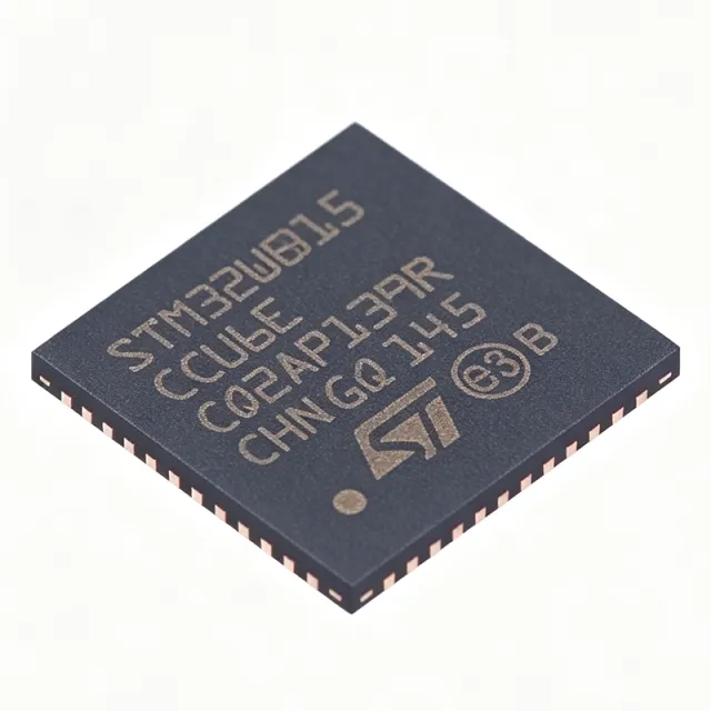
STM32WB15CCU6 - 2.4GHz BLE 5.2 Wireless MCU, 320KB Flash | STMicroelectronics
The STMicroelectronics STM32WB15CCU6 is a dual-core wireless microcontroller integrating a 64 MHz Arm Cortex-M4 application processor and a 32 MHz Arm Cortex-M0+ radio processor, designed for Bluetooth Low Energy 5.2 applications. It features 320 KB of flash memory and 48 KB of SRAM, housed in a 48-pin UFQFPN (UFQFPN-48) package with dimensions of 7x7 mm. The device supports a supply voltage range of 1.71V to 3.6V and operates over a temperature range of -40°C to +105°C, making it suitable for industrial and consumer IoT applications. A wireless microcontroller (MCU) is a system-on-chip that integrates a general-purpose microcontroller core with a radio transceiver, enabling wireless communication protocols such as Bluetooth Low Energy, Zigbee, or proprietary sub-GHz protocols. In the system hierarchy, a wireless MCU sits above a standalone MCU and below a full application processor, providing a balance of processing capability, low power consumption, and wireless connectivity. The STM32WB15CCU6 specifically targets Bluetooth Low Energy 5.2, offering a complete solution for connected devices without requiring an external radio chip. Key features of the STM32WB15CCU6 include a 2.4 GHz radio supporting Bluetooth Low Energy 5.2 with a transmit power of up to +6 dBm and a receiver sensitivity of -96 dBm, ensuring robust wireless links. The dual-core architecture allows the Cortex-M0+ to handle the radio stack independently, freeing the Cortex-M4 for application tasks, which improves real-time performance and reduces power consumption. The device also includes a rich set of peripherals, including multiple UART, SPI, I2C interfaces, a 12-bit ADC, and a random number generator, providing flexibility for various sensor and control applications. From a technical depth perspective, the STM32WB15CCU6 leverages ST's advanced 40nm process technology, enabling low power consumption with multiple low-power modes, including a standby mode with a current consumption of only 1.6 µA. The radio architecture includes a dedicated hardware encryption engine supporting AES-128, AES-256, and other algorithms, ensuring secure wireless communication. The device also features a true random number generator (TRNG) and a unique 96-bit ID, enhancing security for IoT applications. Typical applications include smart home devices such as smart locks, sensors, and lighting controls, as well as healthcare wearables, industrial wireless sensor networks, and asset tracking systems. The STM32WB15CCU6's low power consumption and robust wireless performance make it ideal for battery-powered devices that require long operational lifetimes. When designing with this device, ensure proper antenna matching and PCB layout for the 2.4 GHz radio to achieve optimal range and reliability. The device requires a 32.768 kHz crystal for the low-power RTC and a 32 MHz crystal for the radio, and careful attention to power supply decoupling is essential to minimize noise and ensure stable operation.
STM32WB55RGV6 - Dual-Core BLE 5.3 MCU 1MB Flash | STMicroelectronics
The STMicroelectronics STM32WB55RGV6 is an ultra-low-power multiprotocol wireless microcontroller with a dual-core architecture - an Arm Cortex-M4 with FPU running at 64 MHz for the application and an Arm Cortex-M0+ running at 32 MHz dedicated to the radio stack - with 1 Mbyte of Flash memory, integrated Bluetooth Low Energy 5.3/5.4-compliant and IEEE 802.15.4-2011 radio covering 2.405 GHz to 2.48 GHz, housed in a 68-pin VFQFPN exposed-pad package. A wireless MCU is a microcontroller that integrates both a processing core and a radio transceiver on a single die, sitting at the intersection of the microcontroller and RF transceiver product categories within the broader wireless-connectivity semiconductor hierarchy. By partitioning the real-time radio stack onto the Cortex-M0+ and the user application onto the Cortex-M4, the STM32WB55 family guarantees RF protocol timing independence from application load - a key architectural advantage over single-core BLE MCUs. Key features include 1 MB of Flash and 256 KB of SRAM for application and stack storage, support for Bluetooth 5.3, Thread, and Zigbee protocols on the same silicon, a rich peripheral set (USB 2.0 full-speed device, USART, SPI, I2C, I2S, Quad-SPI, 12-bit ADC, comparators, touch sensing), and ultra-low-power modes with down to a few microamps in Stop 2 with RAM retention. The integrated balun and output power up to +6 dBm (as per family datasheet range) simplify RF front-end design. The dual-core radio architecture offloads BLE/802.15.4 stacks from the application core, so deterministic real-time behavior, security via the Cortex-M0+ trust boundary, and OTA firmware update capability are maintained even under heavy application processing. The 68-pin VFQFPN-EP (7x7 mm class) package provides a good GPIO count for sensor hubs and HMI. Typical applications include smart-home sensors and lighting (Thread/Zigbee), Bluetooth LE beacons and wearables, industrial wireless nodes, and medical monitoring devices. Design consideration: RF layout requires a 50-ohm match to the antenna and solid ground planes on the exposed pad; verify the exact radio output-power and sensitivity figures against the official STM32WB55xx datasheet. This page synthesizes distributor pricing, drop-in alternatives, comparison tables, and design notes not found in the manufacturer datasheet.