Produits (38 000+)

ATMEGA808-XF - 20MHz 8KB Flash AVR MCU 28-SSOP | Microchip
ATMEGA808-XF

ATMEGA808-XF - 20MHz 8KB Flash AVR MCU 28-SSOP | Microchip

The Microchip Technology ATMEGA808-XF is an 8-bit AVR megaAVR 0-series microcontroller featuring a 20 MHz AVR processor with hardware multiplier, 8 KB Flash, 1 KB SRAM, and 256 bytes of EEPROM, housed in a 28-pin SSOP (XF) surface-mount package. The part is positioned by Microchip with Functional Safety (FuSa) support, making it suitable for safety-oriented embedded designs. A microcontroller (MCU) is a single-chip computer that integrates a processor core, program memory (Flash), data memory (SRAM), non-volatile EEPROM, and peripherals such as timers, USARTs, and ADCs on one die. Microcontrollers sit at the lowest level of the embedded-computing hierarchy - below application processors and system-on-chip devices - and are the workhorses of industrial control, appliances, and IoT sensor nodes. Key features of the ATMEGA808-XF include the latest AVR Core Independent Peripherals (CIPs), which allow peripherals such as timers and communication blocks to operate without CPU intervention; a hardware multiplier that accelerates math-heavy code; operation up to 20 MHz; and a memory configuration of 8 KB Flash, 1 KB SRAM, and 256 B EEPROM. The megaAVR 0-series architecture also brings modern peripherals and single-cycle I/O typical of the AVR family. Technically, the megaAVR 0-series uses the enhanced 8-bit AVR RISC core with a two-stage pipeline, executing most instructions in a single clock cycle. The Core Independent Peripherals offload real-time tasks from software, improving determinism - a key reason the family carries Functional Safety documentation support. Peripheral Event System routing allows analog comparators, timers, and custom logic blocks to interconnect without CPU loading. Typical applications include industrial automation nodes, home appliances, IoT sensor endpoints, motor-control辅助 logic, and general-purpose embedded control where a 5 V-tolerant, robust 8-bit MCU in a compact 28-SSOP footprint is preferred. When designing with the ATMEGA808-XF, use the single-pin UPDI interface for programming and debugging to conserve board pins, and verify supply-range, peripheral count, and temperature-grade details against the official Microchip datasheet before finalizing the design. This page synthesizes distributor availability, same-family drop-in alternatives (ATmega809/1608/3208/4808 in the same 28-SSOP XF package), and practical design guidance not consolidated in the manufacturer datasheet.

Devis Contact
ATMEGA808-XU - 8-Bit AVR MCU 20MHz 8KB Flash | Microchip
ATMEGA808-XU

ATMEGA808-XU - 8-Bit AVR MCU 20MHz 8KB Flash | Microchip

The Microchip Technology ATMEGA808-XU is an 8-bit megaAVR 0-series microcontroller with hardware multiplier, running at up to 20 MHz, with 8 KB Flash, 1 KB SRAM and 256 bytes of EEPROM, housed in a 28-pin SSOP (SOIC-outline) surface-mount package rated for -40C to +125C industrial operation. A microcontroller (MCU) integrates a processor core, non-volatile program memory, RAM, and peripherals onto a single chip, sitting at the top of the hierarchy that runs from discrete transistors through logic ICs to full system-on-chip devices. The megaAVR 0-series is Microchip's modernized AVR family using the latest Core Independent Peripherals, enabling low-power operation without CPU intervention. Key features include the AVR RISC core with hardware multiplier executing most instructions in a single cycle, up to 20 MHz operation, 8 KB of self-programmable Flash, and functional-safety (FuSa) support documented by Microchip. Peripherals include Core Independent Peripherals (CIPs) such as configurable timers, USART, and analog comparators that operate without CPU overhead, reducing firmware complexity and interrupt latency. The 0-series architecture uses a unified address space and single-cycle I/O access. The hardware multiplier accelerates math-intensive loops common in motor control and metering firmware. Multiple sleep modes and peripheral clock gating allow very low average power in battery-operated nodes; the event system routes peripheral signals directly to other peripherals without CPU involvement. Typical applications include industrial control and sensing nodes, home appliances, consumer electronics, and functional-safety-oriented designs that benefit from Microchip's FuSa documentation package. The 28-SSOP package fits compact 2-layer PCBs where hand or wave soldering of fine-pitch QFN is undesirable. Designers should verify the exact temperature grade: the -XU suffix indicates the -40C to +125C industrial range, while -XF variants cover -40C to +105C; both share the same SSOP-28 footprint. Supply voltage, peripheral counts, and full electrical characteristics should be confirmed in the official Microchip ATmega808 datasheet before final design freeze. This page synthesizes distributor listings, drop-in alternative data, and engineering selection guidance not found in the manufacturer datasheet, helping engineers source and qualify the ATMEGA808-XU faster.

Devis Contact
ATMEGA809-AF - 8-bit AVR MCU 20MHz 8KB Flash 48-TQFP | Microchip
ATMEGA809-AF

ATMEGA809-AF - 8-bit AVR MCU 20MHz 8KB Flash 48-TQFP | Microchip

The Microchip Technology ATMEGA809-AF is an 8-bit megaAVR 0 series microcontroller featuring the AVR processor with hardware multiplier, running at up to 20 MHz with 8 KB Flash, 1 KB SRAM and 256 bytes of EEPROM, housed in a 48-pin TQFP (7x7 mm) package. An 8-bit microcontroller (MCU) integrates a processor core, memory, and peripherals on a single chip, forming the lowest tier of the embedded controller hierarchy: MCU -> embedded processor -> system-on-chip. The megaAVR 0 series is Microchip's latest generation of AVR devices, replacing the classic megaAVR line with Core Independent Peripherals (CIPs), an Event System, and intelligent analog. Because peripherals operate without CPU intervention, real-time tasks continue even while the core sleeps, which reduces power consumption and firmware complexity. Key features of the ATMEGA809-AF include the 20 MHz AVR core with a hardware multiplier for efficient integer math, 8 KB of self-programmable Flash memory, 1 KB SRAM, and 256 bytes of separate EEPROM for data retention across power cycles. The device operates from a single supply in the 1.8 V to 5.5 V range, giving wide design headroom for battery and industrial 5 V systems. The Peripheral Touch Controller (PTC) supports capacitive touch buttons and sliders without external components, and the 10-bit ADC plus analog comparators cover most sensing needs. Architecturally, the Event System routes peripheral signals to other peripherals without CPU loading, enabling deterministic low-latency control. The device integrates USART, SPI, and TWI (I2C) serial interfaces, multiple 16-bit timers with PWM outputs, a watchdog timer, and CRC-SCAN hardware. Functional Safety (FuSa) documentation support makes it suitable for safety-oriented industrial designs. Typical applications include industrial automation and control panels, home appliances and HVAC control boards, capacitive-touch user interfaces, and low-power battery-operated sensor nodes. The 48-pin TQFP offers generous GPIO count for keypads, LEDs, and displays. When designing with this part, remember that the UPDI (Unified Program and Debug Interface) uses one pin for programming, freeing board space compared with legacy ISP headers; flash writes are self-programmable for field updates. This page synthesizes distributor pricing, drop-in same-family alternatives, design notes, and AEO-optimized FAQs not consolidated in the manufacturer datasheet.

Devis Contact
ATMEGA809-AFR - 8-Bit AVR MCU 20MHz 8KB Flash 48-TQFP | Microchip
ATMEGA809-AFR

ATMEGA809-AFR - 8-Bit AVR MCU 20MHz 8KB Flash 48-TQFP | Microchip

The Microchip Technology ATMEGA809-AFR is an 8-bit megaAVR 0-series microcontroller with a 20 MHz AVR processor featuring a hardware multiplier, 8 KB of Flash memory, 1 KB of SRAM, and 256 bytes of EEPROM, housed in a 48-pin TQFP (7x7 mm) package. It operates from a 1.8V to 5.5V supply, making it suitable for both 3.3V and 5V systems. An 8-bit microcontroller (MCU) integrates a processor core, memory, and peripherals on a single chip, sitting at the lowest level of the embedded-systems hierarchy: MCU -> embedded processor -> system-on-chip. The megaAVR 0-series is Microchip's modernized AVR family, and the ATmega809 is its entry-density 48-pin member. Key features include the AVR RISC core with a single-cycle hardware multiplier executing most instructions in one clock cycle, Core Independent Peripherals (CIPs) that operate without CPU intervention, and a configurable Event System that routes peripheral signals internally. Peripherals include a 10-bit ADC, analog comparators, multiple 16-bit timers, USARTs, SPI, and TWI (I2C). Functional Safety (FuSa) support positions it for safety-relevant designs. Architecturally, the device uses a modified Harvard architecture with separate program and data buses, single-level instruction pipelining, and low-power sleep modes down to sub-microamp levels. Memory is organized as 8K x 8 Flash with in-system self-programming, plus 256 bytes of nonvolatile EEPROM for calibration data. Typical applications include industrial automation nodes, home appliances, IoT sensor endpoints, motor control auxiliaries, and consumer electronics where the 48-pin count supports multiple communication ports. Design consideration: keep the AVDD/decoupling layout per the datasheet, and note the PA0/UPDI multiplexing when planning debug access. This page adds value beyond the datasheet with tiered distributor pricing (as of 2026-09-18), drop-in family alternatives, pinout data, and application guidance for the megaAVR 0-series.

Devis Contact
ATMEGA809-AU - 8-Bit AVR MCU 20MHz 8KB Flash | Microchip
ATMEGA809-AU

ATMEGA809-AU - 8-Bit AVR MCU 20MHz 8KB Flash | Microchip

The Microchip Technology ATMEGA809-AU is an 8-bit megaAVR 0-series microcontroller with an AVR processor with hardware multiplier, running at up to 20 MHz and integrating 8 KB Flash, 1 KB SRAM, and 256 bytes of EEPROM in a 48-pin TQFP (7x7 mm) package. The device is Functional Safety (FuSa) capable per its product classification. An 8-bit microcontroller is an integrated circuit that executes program code on a CPU with an 8-bit-wide data bus, combining flash program memory, SRAM data memory, EEPROM, peripherals, and clocking into a single chip. In the embedded-systems hierarchy, the ATMEGA809-AU sits within the megaAVR family of general-purpose MCUs, which in turn belongs to the broader microcontroller unit (MCU) category of semiconductor devices. Microcontrollers replace multi-chip processor-plus-peripheral designs, reducing board area, bill-of-materials cost, and system power consumption. Key features include the megaAVR 0-series Core Independent Peripherals (CIPs), which include the Event System allowing peripherals to communicate directly without CPU intervention, intelligent analog modules, and advanced low-power features. Connectivity is provided by I2C (TWI), SPI, and UART/USART serial interfaces, supporting multi-drop sensor networks and host communication. Peripheral functions include Brown-out Detect/Reset and Power-on Reset for supply supervision, ensuring reliable startup and operation in noisy electrical environments. Architecturally, the ATMEGA809-AU uses the AVR RISC core with a hardware multiplier, enabling single-cycle arithmetic for digital control and signal-processing tasks while executing code from 8 KB of flash. The 1 KB SRAM provides workspace for program variables and communication buffers, while the 256-byte EEPROM retains calibration data and configuration through power cycles. Supply supervision peripherals such as BOD keep the core within safe operating margins across the full voltage and temperature range. Typical applications include industrial automation nodes, home-appliance control boards, IoT sensor endpoints, and motor-control or LED-lighting systems where an efficient 8-bit MCU with robust analog and safety supervision is required at low cost. When designing with the ATMEGA809-AU, use the single-pin UPDI interface (shared with PORTF) for programming and debugging to minimize external tooling overhead, and configure Brown-out Detection to match the supply rail's droop characteristics. Decouple VDD pins with 100 nF ceramics placed close to the package. This page synthesizes distributor pricing, drop-in family alternatives, pinout data, and practical design guidance not consolidated in the manufacturer datasheet, verified against DigiKey, Mouser, LCSC, and Microchip sources as of 2026-09-18.

Devis Contact
ATMEGA809-AUR - 8KB AVR MCU 20MHz TQFP-48 | Microchip
ATMEGA809-AUR

ATMEGA809-AUR - 8KB AVR MCU 20MHz TQFP-48 | Microchip

The Microchip Technology ATMEGA809-AUR is an 8-bit AVR megaAVR 0-series microcontroller featuring a 20 MHz AVR processor with hardware multiplier, 8 KB of Flash memory, 1 KB of SRAM and 256 bytes of EEPROM, packaged in a 48-pin TQFP (7x7 mm) with tape-and-reel delivery and an industrial temperature grade. A microcontroller (MCU) is a single integrated circuit that combines a processor core, program memory, data memory and peripherals into one chip, sitting at the lowest level of the embedded-system hierarchy: microcontroller -> embedded processor -> system-on-chip -> computing system. The megaAVR 0-series is Microchip's modern AVR family built around Core Independent Peripherals, meaning timers, comparators and communication blocks can operate without CPU intervention via the Event System. Key features include the 8 KB self-programming Flash with EEPROM emulation, 1 KB SRAM, a 10-bit ADC with up to 16 multiplexed channels, three USARTs, and hardware multiplier support for efficient 8x8 arithmetic. The AVR core executes most instructions in a single cycle, delivering strong real-time determinism at 20 MHz. Technical depth comes from the Event System, which routes peripheral signals (timer overflows, ADC results, comparator outputs) directly to other peripherals without CPU load, reducing latency and power. Sleep modes down to microamp levels, a configurable low-frequency oscillator, and a Peripheral Touch Controller support low-power and capacitive-touch designs. Functional Safety (FuSa) documentation is available for safety-oriented applications. Typical applications include industrial control and automation nodes, consumer appliance interfaces, motor-control辅助 logic, and IoT sensor end nodes where 20 MHz 8-bit performance, low power and rich analog peripherals fit the bill. Design consideration: the ATMEGA809-AUR is supplied in the 48-pin TQFP (7x7), so plan a decoupling capacitor on each VDD pin and route the single-wire UPDI debug/programming pin to a header for in-system programming. This page synthesizes distributor pricing, drop-in megaAVR 0-series alternatives, and practical design notes not found in the manufacturer datasheet alone.

Devis Contact
ATMEGA809-MF - 8-Bit AVR MCU 20MHz 8KB Flash | Microchip
ATMEGA809-MF

ATMEGA809-MF - 8-Bit AVR MCU 20MHz 8KB Flash | Microchip

The Microchip Technology ATMEGA809-MF is an 8-bit AVR megaAVR 0-series microcontroller with hardware multiplier, running at up to 20 MHz with 8 KB Flash, 1 KB SRAM, and 256 bytes of EEPROM, housed in a 48-pin VQFN (6x6 mm) exposed-pad package and rated from -40C to +125C as part of the Functional Safety (FuSa) supporting family. A microcontroller (MCU) is a single integrated circuit that combines a processor core, program memory, data memory, and peripherals into one chip, sitting at the heart of embedded systems within the broader hierarchy of semiconductors -> integrated circuits -> embedded processors. The megaAVR 0 series is Microchip's modernized AVR line featuring Core Independent Peripherals (CIPs) that operate without CPU intervention. Key features include the 20 MHz AVR CPU with a hardware multiplier for efficient arithmetic, an Event System that routes peripheral signals internally without CPU load, intelligent analog comprising a 10-bit ADC with up to 12 input channels and comparators, and low-power modes for battery-operated designs. The 8 KB self-programming Flash supports bootloaders, and CRC-capable memory access supports functional-safety workflows. Architecturally, the ATmega809 uses the enhanced AVR RISC core with a mostly single-cycle instruction set, single-cycle I/O access, and peripherals including USARTs, SPI, TWI (I2C), timers with capture/compare/PWM, and a Configurable Custom Logic (CCL) block. The FuSa designation means the family is supported by safety documentation for IEC 60730/UL 60730 class applications. Typical applications include home appliances, industrial automation nodes, motor control辅助 boards, and IoT sensor endpoints where deterministic 8-bit control and low BOM cost matter. Design consideration: the 6x6 VQFN exposed pad should be soldered to a grounded copper pour for thermal dissipation and signal integrity; remember PA0 is shared with UPDI programming. This page synthesizes distributor pricing, drop-in family alternatives, and design notes not found in the manufacturer datasheet. Pricing shown as of 2026-09-18.

Devis Contact
ATMEGA809-MFR - 8-bit AVR MCU 20MHz 8KB Flash | Microchip
ATMEGA809-MFR

ATMEGA809-MFR - 8-bit AVR MCU 20MHz 8KB Flash | Microchip

The Microchip ATMEGA809-MFR is an 8-bit megaAVR 0-series microcontroller featuring the AVR processor with hardware multiplier, running at up to 20 MHz, with 8 KB Flash, 1 KB SRAM and 256 bytes of EEPROM in a 48-pin VQFN (6x6 mm) package. It is a Functional Safety (FuSa) qualified, automotive temperature grade MCU. An 8-bit AVR microcontroller is a single-chip computer that integrates a RISC processor core, program Flash memory, SRAM, EEPROM and peripherals such as UART, SPI, I2C/TWI, timers and ADC into one package. Within the power-management and embedded-control hierarchy, microcontrollers sit above discrete logic and below application processors, executing real-time control tasks in industrial, automotive and consumer systems. Key features include the Core Independent Peripherals (CIPs) such as the Event System that routes signals between peripherals without CPU intervention, intelligent analog blocks, and advanced low-power modes. The hardware multiplier accelerates math-intensive loops, while the 20 MHz maximum clock delivers efficient processing for the megaAVR 0 family. Technically, the ATmega809 belongs to the megaAVR 0-series (ATmega808/809/1608/1609/3208/3209/4808/4809) sharing a common peripheral set, so code written for the ATmega809 scales upward to larger Flash variants with minimal changes. The FuSa qualification supports safety-critical development flows, and the automotive temperature grade extends operation to harsh environments. Typical applications include industrial automation sensor nodes, automotive body and comfort control modules, and IoT smart-home endpoints, where the combination of 8 KB Flash, CIPs and low-power sleep modes reduces system cost and energy consumption. A key design consideration is voltage range and clock scaling: verify that your operating frequency is permitted at the lowest supply voltage in your system, and use the Event System to offload time-critical signaling from the CPU for deterministic latency. This page synthesizes distributor pricing, drop-in same-family alternatives, practical design notes and application guidance not found in the manufacturer datasheet, as of 2026-09-18.

Devis Contact
ATMEGA809-MU - 8KB AVR MCU 20MHz VQFN-48 | Microchip (Tape & Reel)
ATMEGA809-MU

ATMEGA809-MU - 8KB AVR MCU 20MHz VQFN-48 | Microchip (Tape & Reel)

The Microchip Technology ATMEGA809-MU is an 8-bit AVR megaAVR 0-series microcontroller running at up to 20 MHz with 8 KB Flash, 1 KB SRAM, and 256 bytes of EEPROM, housed in a 48-pin VQFN (6x6 mm) surface-mount package with exposed pad. It operates from 1.8 V to 5.5 V over an industrial -40 C to +85 C temperature range and integrates a 10-bit ADC with 41 programmable I/O lines. A microcontroller (MCU) is a single-chip computer that combines a processor core, memory, and peripherals on one die, forming the lowest layer of the embedded-systems hierarchy: MCU -> embedded processor -> computing system. The megaAVR 0 family succeeds the classic ATmega line, adding Core Independent Peripherals (CIPs) that run without CPU intervention, improving real-time determinism and reducing firmware complexity. Key differentiating features include the hardware multiplier in the AVR RISC core, the Event System for peripheral-to-peripheral signaling without CPU load, and Functional Safety (FuSa) documentation support for IEC 61508 and ISO 26262 oriented designs. Intelligent analog comprises the 10-bit ADC and analog comparators, while flexible timers, USARTs, SPI, and TWI (I2C) interfaces cover most connectivity needs. Technically, the AVR 8-bit RISC Harvard architecture executes most instructions in a single cycle, delivering up to 20 MIPS at 20 MHz. The MUR ordering code denotes the 48-pin VQFN-EP (6x6) package in Tape and Reel packing; single-cycle multiply and rich interrupt structure suit both control and light signal-processing tasks. Typical applications include industrial automation nodes, IoT sensor endpoints, motor control assistants, consumer appliance control, and functional-safety-adjacent monitoring circuits where 8 KB of code space, low power modes, and CIP autonomy are sufficient. Design consideration: choose the smallest Flash variant (this 8 KB part) only after confirming code growth headroom; the pin-compatible ATmega1609/3209/4809 allow migration without PCB changes. This page synthesizes distributor pricing, pin-compatible family alternatives, and design guidance not consolidated in the manufacturer datasheet.

Devis Contact
ATMEGA809-MUR - 8KB AVR MCU 20MHz VQFN-48 | Microchip
ATMEGA809-MUR

ATMEGA809-MUR - 8KB AVR MCU 20MHz VQFN-48 | Microchip

The Microchip Technology ATMEGA809-MUR is an 8-bit AVR megaAVR 0-series microcontroller running at up to 20 MHz with 8 KB Flash, 1 KB SRAM, and 256 bytes of EEPROM, housed in a 48-pin VQFN (6x6 mm) surface-mount package with exposed pad. It operates from 1.8 V to 5.5 V over an industrial -40 C to +85 C temperature range and integrates a 10-bit ADC with 41 programmable I/O lines. A microcontroller (MCU) is a single-chip computer that combines a processor core, memory, and peripherals on one die, forming the lowest layer of the embedded-systems hierarchy: MCU -> embedded processor -> computing system. The megaAVR 0 family succeeds the classic ATmega line, adding Core Independent Peripherals (CIPs) that run without CPU intervention, improving real-time determinism and reducing firmware complexity. Key differentiating features include the hardware multiplier in the AVR RISC core, the Event System for peripheral-to-peripheral signaling without CPU load, and Functional Safety (FuSa) documentation support for IEC 61508 and ISO 26262 oriented designs. Intelligent analog comprises the 10-bit ADC and analog comparators, while flexible timers, USARTs, SPI, and TWI (I2C) interfaces cover most connectivity needs. Technically, the AVR 8-bit RISC Harvard architecture executes most instructions in a single cycle, delivering up to 20 MIPS at 20 MHz. The MUR ordering code denotes the 48-pin VQFN-EP (6x6) package in Tape and Reel packing; single-cycle multiply and rich interrupt structure suit both control and light signal-processing tasks. Typical applications include industrial automation nodes, IoT sensor endpoints, motor control assistants, consumer appliance control, and functional-safety-adjacent monitoring circuits where 8 KB of code space, low power modes, and CIP autonomy are sufficient. Design consideration: choose the smallest Flash variant (this 8 KB part) only after confirming code growth headroom; the pin-compatible ATmega1609/3209/4809 allow migration without PCB changes. This page synthesizes distributor pricing, pin-compatible family alternatives, and design guidance not consolidated in the manufacturer datasheet.

Devis Contact
ATMEGA8515-16AC - 8-bit AVR MCU 16MHz 8KB Flash | Microchip
ATMEGA8515-16AC

ATMEGA8515-16AC - 8-bit AVR MCU 16MHz 8KB Flash | Microchip

The Microchip Technology ATMEGA8515-16AC is a low-power 8-bit AVR RISC microcontroller featuring 16 MIPS throughput at 16 MHz, 8 KB In-System Programmable Flash, and 512 bytes each of EEPROM and internal SRAM, housed in a 44-pin TQFP (10x10 mm) surface-mount package. A microcontroller unit (MCU) integrates a processor core, program memory, data memory, and peripherals on a single die, sitting at the top of the embedded-control hierarchy (MCU -> embedded processor -> integrated circuit -> semiconductor). The AVR family uses an enhanced Harvard RISC architecture in which most of its 130 instructions execute in a single clock cycle, and 32 general-purpose working registers are directly connected to the ALU. Key features include 8 KB self-programming Flash with Read-While-Write capability, up to 64 KB of external memory expansion through a parallel External Memory Interface (EBI/EMI), 35 general-purpose I/O lines, and connectivity via SPI, USART, and TWI (I2C-compatible) interfaces. Two flexible Timer/Counters with compare modes, internal and external interrupt sources, and a programmable Watchdog Timer round out the peripheral set. The 16AC speed grade sustains full 16 MHz operation at a commercial temperature range with a 4.5V to 5.5V supply. Architecturally, the single-stage pipelined AVR core fetches one instruction while executing the next, achieving near one-MIPS-per-MHz efficiency. Fully static operation allows clocking down to DC for ultra-low-power sleep modes without register loss, while self-programming Flash enables field firmware updates and bootloaders. Typical applications include industrial control panels using the external memory interface, legacy AVR system maintenance and repair, and motor/actuator control leveraging the timer compare outputs. Design tip: if your firmware uses less than 8 KB Flash and no external bus, pin-compatible higher-density family members reduce obsolescence risk; always verify the JTAG and EBI pin mapping before board reuse. This page synthesizes distributor availability data, drop-in alternative options, and practical design guidance not consolidated in the manufacturer datasheet. Pricing shown is as of 2026-09-18.

Devis Contact
ATMEGA8515-16AI - 8-bit AVR MCU, 16MHz, 8KB Flash, 44-TQFP | Microchip
ATMEGA8515-16AI

ATMEGA8515-16AI - 8-bit AVR MCU, 16MHz, 8KB Flash, 44-TQFP | Microchip

The Microchip (originally Atmel) ATMEGA8515-16AI is an 8-bit high-performance, low-power AVR RISC-based microcontroller (MCU) featuring 16 MHz maximum clock speed, 8 KB of in-system programmable Flash, 544 bytes SRAM, 512 bytes EEPROM, and support for up to 64 KB external SRAM, packaged in a 44-pin TQFP (10x10 mm) industrial-temperature grade (-40C to +85C) footprint. An 8-bit microcontroller is a single-chip computer that integrates a CPU core, program memory (Flash), data memory (RAM), non-volatile storage (EEPROM), and I/O peripherals on one die. It belongs to the broader family of embedded microcontrollers (MCUs), which are sub-classified as RISC (Reduced Instruction Set Computer) vs CISC architectures; the AVR core is a Harvard-architecture RISC design that executes most instructions in a single clock cycle. Within power-managed electronics, MCUs sit hierarchically below microprocessors and above discrete logic ICs, providing deterministic real-time control with low quiescent power. Key differentiating features of the ATMEGA8515-16AI include 130 powerful AVR instructions (most single-cycle), 32 general-purpose working registers, fully static operation, throughput approaching 16 MIPS at 16 MHz, an 8-channel 10-bit ADC, two 8-bit timer/counters plus one 16-bit timer/counter, a programmable watchdog timer with separate on-chip oscillator, and rich connectivity peripherals including SPI, UART, and TWI (Two-Wire Interface, I2C-compatible). The device supports 6 sleep modes (Idle, Power-save, Power-down, Standby, Extended Standby, and ADC Noise Reduction) enabling <1 uA power-down current, which is critical for battery-powered and energy-harvesting systems. Industrial-grade temperature range and self-programmable Flash for field firmware updates make it suitable for long-life industrial designs. Architecturally, the ATmega8515 uses an enhanced AVR RISC core with a 2-stage pipelined Harvard bus, allowing instruction fetch and data access to occur in parallel. The integrated 10-bit successive-approximation ADC provides 8 single-ended channels with optional differential mode, and the on-chip analog comparator enables mixed-signal feedback without external components. The brown-out detector and internal calibrated RC oscillator reduce BOM cost while improving reliability. Typical applications for the ATMEGA8515-16AI include industrial control systems, sensor interfacing nodes, low-power embedded sensors, communication bridges, motor control for small BLDC/stepper subsystems, USB-to-UART bridges, HVAC controllers, building automation, and any cost-sensitive embedded application requiring deterministic real-time control with low power consumption. When designing with the ATMEGA8515-16AI, mind the 16 MHz speed grade (the '-16A' suffix specifies this) and ensure VCC is held within 4.5V to 5.5V at full speed; for 3.3V operation consider the ATMEGA8515L-8 family. Verify ISP programming pin assignments and ensure decoupling caps are placed close to the AVCC and VCC pins. This page synthesizes distributor pricing, drop-in alternatives, and practical design notes not found in the manufacturer datasheet.

Devis Contact
ATMEGA8515-16AJ - 8KB Flash AVR MCU 16MHz TQFP-44 | Microchip
ATMEGA8515-16AJ

ATMEGA8515-16AJ - 8KB Flash AVR MCU 16MHz TQFP-44 | Microchip

The Microchip ATMEGA8515-16AJ is a high-performance, low-power 8-bit AVR RISC microcontroller with 8 KB In-System Programmable Flash, 512 bytes EEPROM, 512 bytes internal SRAM with support for up to 64 KB external SRAM, and 16 MIPS throughput at 16 MHz, housed in a 44-pin TQFP package with industrial temperature range. A microcontroller is a complete computing system on a single chip, combining a processor core, program memory, data memory, and peripherals. The ATmega8515 belongs to the 8-bit AVR RISC family, which sits within Microchip Technology's broader MCU portfolio of embedded processors. Its 130-instruction RISC architecture executes most instructions in a single clock cycle, and 32 general purpose working registers are directly connected to the ALU, delivering up to 16 MIPS at 16 MHz. Key differentiating features include the external memory interface - rare among small AVRs - which expands SRAM to 64 KB for data-heavy applications. The peripheral set covers two flexible Timer/Counters with compare modes, a programmable Serial USART, a programmable Watchdog Timer with internal oscillator, an SPI serial interface, and 35 general purpose I/O lines. Architecturally, the ATmega8515 uses a Harvard structure with separate program and data buses, enabling Read-While-Write self-programming Flash operation. The self-programming capability supports field firmware updates without an external programmer, while the enhanced power-save modes reduce consumption in battery-powered systems. Typical applications include industrial control panels, legacy 8051-pinout system migrations (the ATmega8515 is 8051 pin-compatible in 44-pin packages), data loggers using external SRAM, embedded test equipment, and motor-adjacent control logic driven by the timer compare outputs. Design-wise, the J suffix denotes a lead-free TQFP package; the A suffix identifies the ATmega8515A silicon revision, so always confirm bootloader and fuse compatibility with the A-variant datasheet when migrating from original ATmega8515 parts. This page synthesizes distributor availability, verified drop-in alternatives, and practical design guidance not consolidated in the manufacturer datasheet.

Devis Contact
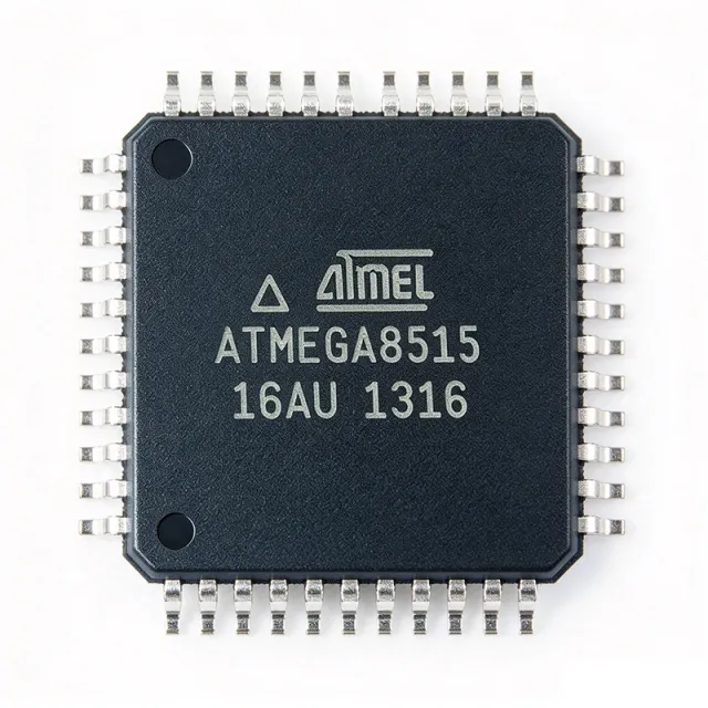
ATMEGA8515-16AU - 8-bit AVR MCU 16MHz 8KB Flash 44-TQFP
ATMEGA8515-16AU

ATMEGA8515-16AU - 8-bit AVR MCU 16MHz 8KB Flash 44-TQFP

The Microchip Technology (formerly Atmel) ATMEGA8515-16AU is an 8-bit AVR RISC microcontroller delivering 16 MIPS throughput at 16 MHz, with 8 KB of in-system programmable Flash, 512 B SRAM, 512 B EEPROM, and an external SRAM interface supporting up to 64 KB, housed in a 44-pin TQFP (10x10 mm) surface-mount package. Background Knowledge: An 8-bit microcontroller (MCU) is a single-chip computer integrating a CPU core, program memory, data memory, and peripherals around an 8-bit data bus. The ATmega8515 belongs to the AVR enhanced RISC family — a Harvard-architecture core that executes most instructions in a single clock cycle, achieving roughly 1 MIPS per MHz. Within the broader taxonomy, it sits as: 8-bit microcontroller -> microcontroller -> embedded processor -> semiconductor. The RISC (Reduced Instruction Set Computer) approach trades a larger, fixed-length instruction set for simpler, faster pipeline execution, making AVR MCUs popular in hobbyist, industrial, and educational designs. Key differentiating features of this part include: 130 powerful RISC instructions (most single-cycle), 35 programmable I/O lines, two 8-bit timer/counters plus one 16-bit timer/counter, a full-duplex hardware USART, an SPI serial interface, an analog comparator, programmable watchdog timer with on-chip oscillator, and six sleep modes for power optimization. The device operates from 4.5 V to 5.5 V (the “16” speed grade at 16 MHz). Technical depth: The AVR core uses on-chip Flash for program storage, allowing in-system programming via SPI or parallel modes. The 64 KB external SRAM interface is multiplexed and supports both SRAM and memory-mapped peripherals, enabling designs that require more RAM than the on-chip 512 B can provide. The internal bandgap reference and on-chip calibrated RC oscillator reduce external component count, while the JTAG (IEEE 1149.1-compliant) interface supports on-chip debug via tools such as the AVR JTAGICE or Atmel-ICE. Typical applications include industrial control systems, sensor interface nodes, human-machine interface (HMI) front panels, building automation controllers, and Arduino-compatible firmware development through community packages such as MCUdude MajorCore. The wide operating voltage and robust I/O drive capability also suit automotive body electronics and white-goods appliance controllers. When designing with this part, ensure the external SRAM interface traces are kept short and the AVCC pin is properly decoupled (100 nF + 10 µF) to avoid ADC noise coupling — even if the ADC is unused. The reset pin should be pulled up with a 10 kΩ resistor to VCC and fitted with a 100 nF capacitor to ground for noise immunity. This page synthesizes distributor pricing, drop-in alternatives, design notes, and pin-level information not consolidated on a single manufacturer datasheet — supporting engineers evaluating the ATmega8515 for new designs or as a long-term supply alternative to newer ATmega variants.

USD $2,85 En stock
ATMEGA8515-16AUR - AVR MCU 8KB Flash 16MHz TQFP-44 | Microchip
ATMEGA8515-16AUR

ATMEGA8515-16AUR - AVR MCU 8KB Flash 16MHz TQFP-44 | Microchip

The Microchip Technology ATMEGA8515-16AUR is an 8-bit AVR RISC microcontroller with 8 KB in-system programmable Flash, 512 B EEPROM, 512 B internal SRAM (expandable to 64 KB external SRAM), 16 MHz maximum clock (16 MIPS throughput) and an industrial-range 44-pin TQFP surface-mount package. A microcontroller (MCU) integrates a processor core, program memory, data memory and peripherals on a single chip, forming the lowest level of the embedded-system hierarchy: MCU -> embedded processor -> SoC. The ATmega8515 belongs to the AVR family, built on an enhanced RISC architecture where most of its 130 instructions execute in a single clock cycle, achieving roughly 1 MIPS per MHz. Key features include the 8 KB self-programmable Flash with Read-While-Write support, an external memory interface with ALE/WR/RD signals for up to 64 KB of external SRAM, two flexible Timer/Counters with compare and PWM modes, a programmable serial USART, and a programmable Watchdog Timer with on-chip oscillator. The supply voltage range is 4.5 V to 5.5 V for the 16 MHz speed grade, and the AUR suffix denotes the -40C to +85C industrial temperature range in Tape and Reel packaging. Architecturally, the device provides 32 general-purpose working registers directly connected to the ALU, allowing two independent registers to be accessed in one instruction. It offers 35 general-purpose I/O lines, internal and external interrupt sources, and SPI programming capability. Peripherals include Timer/Counter0 (8-bit with PWM) and Timer/Counter1 (16-bit with input capture, compare and PWM), plus a dedicated PWM channel on OC1A/OC1B/OC0 outputs. Typical applications include legacy industrial control boards, motor-control and power-inverter front panels, point-of-sale peripherals, and educational/embedded training platforms where 5 V logic levels simplify interfacing with sensors and relays. Design tip: because the 4.5 V to 5.5 V supply is mandatory at 16 MHz, 3.3 V designs must use the ATmega8515L-8AUR speed grade or a different family member. Decouple VCC/AVCC with 0.1 uF ceramics placed within 5 mm of the pins. This page adds value beyond the manufacturer datasheet (document 2512S) by consolidating distributor pricing, drop-in alternative analysis against the ATmega162, and practical design notes for legacy AVR designs.

Devis Contact
ATMEGA8515-16JC - 8-bit AVR MCU 8KB Flash 16MHz | Microchip
ATMEGA8515-16JC

ATMEGA8515-16JC - 8-bit AVR MCU 8KB Flash 16MHz | Microchip

The Microchip Technology ATMEGA8515-16JC is a high-performance, low-power 8-bit AVR RISC microcontroller with 8 KB of In-System Programmable Flash, 512 bytes of EEPROM, 544 bytes of internal SRAM, and support for up to 64 KB of external SRAM, executing up to 16 MIPS at 16 MHz in a 44-pin PLCC (J-Lead) package. A microcontroller (MCU) is a single-chip computer that integrates a processor core, program memory, data memory, and peripherals on one die, sitting at the device level of the embedded-systems hierarchy (semiconductor -> integrated circuit -> microcontroller -> embedded system). The AVR family uses a modified Harvard RISC architecture in which most of its 130 instructions execute in a single clock cycle, giving predictable, high-throughput execution for real-time control tasks. Key features of the ATMEGA8515-16JC include 35 programmable I/O lines, an External Bus Interface (EBI/EMI) with ALE, WR and RD strobes for expanding to 64 KB of external memory, SPI and UART/USART serial interfaces, three hardware timers (two 8-bit and one 16-bit), and an 8-channel 10-bit ADC. The device operates from a 4.5 V to 5.5 V supply at 16 MHz (the -16 speed grade), with an operating temperature range of 0 C to +70 C indicated by the C temperature designator. Technical depth: the AVR core is fully static, allowing clock frequencies down to DC without state loss, and the self-programming Flash enables field firmware updates through bootloader code. In-circuit programming via SPI and debugging through JTAG-adjacent AVR tools reduce development time. The External Bus Interface multiplexes the PA port as an address/data bus with PC providing address lines A8-A15. Typical applications include industrial control systems, legacy equipment maintenance, motor control boards, test fixtures, and educational/embedded platforms - the Arduino-compatible MajorCore package supports the ATmega8515. The PLCC-44 package suits through-hole-style sockets and PCB rework-friendly layouts. Design consideration: verify supply decoupling with 100 nF ceramics on both supply pins and validate the External Bus Interface timing when running at the full 16 MHz, since external SRAM access adds propagation delays to the bus. This page synthesizes distributor pricing, drop-in alternatives, pinout data, and practical design notes not found in the manufacturer datasheet alone.

Devis Contact
ATMEGA8515-16JI - 8-Bit AVR MCU 16MHz 8KB Flash 44-PLCC | Microchip
ATMEGA8515-16JI

ATMEGA8515-16JI - 8-Bit AVR MCU 16MHz 8KB Flash 44-PLCC | Microchip

The Microchip Technology ATMEGA8515-16JI is an 8-bit AVR RISC microcontroller with 8 KB of In-System Programmable Flash, 512 bytes SRAM (plus up to 64 KB external memory interface), 512 bytes EEPROM, and 16 MIPS throughput at 16 MHz, housed in a 44-pin PLCC (16.6 x 16.6 mm) package. A microcontroller unit (MCU) integrates a processor core, program memory, data memory, and peripherals on a single silicon die, sitting at the center of the embedded-systems hierarchy between bare logic ICs and full application processors. The ATmega8515 belongs to Microchip's (formerly Atmel) AVR ATmega family of 8-bit RISC microcontrollers, which execute most of their 130 instructions in a single clock cycle. Key features include the AVR enhanced RISC architecture with 32 general-purpose working registers, 35 programmable I/O lines, and a full external memory interface up to 64 KB. Peripherals include two flexible Timer/Counters with compare modes, a Serial Programmable USART, a Master/Slave SPI interface, and a programmable Watchdog Timer with on-chip oscillator. Special microcontroller features include In-System Programmable (ISP) Flash with Read-While-Write capability, debugWIRE-compatible on-chip debugging through ICE support, and power-saving Idle and Power-down modes. The -16JI suffix defines the operating envelope: 4.5 V to 5.5 V supply, 0 to 16 MHz operation, and the industrial temperature range of -40C to +85C, making the device suitable for uncontrolled factory and outdoor environments. The self-programming Flash enables field firmware updates over UART or SPI without a parallel programmer. Typical applications include industrial control panels, motor-control front ends, legacy process instrumentation, and communications interface boards that leverage the 44-PLCC through-hole-friendly footprint and 5 V noise immunity. Design consideration: when using the external SRAM interface, reserve ports A and C for address and data buses, leaving only 3 free I/O lines - budget pin usage early. This page synthesizes distributor pricing, drop-in alternatives, and practical design notes not found in the manufacturer datasheet.

Devis Contact
ATMEGA8515-16JU - 8KB AVR MCU 16MHz 44-PLCC | Microchip
ATMEGA8515-16JU

ATMEGA8515-16JU - 8KB AVR MCU 16MHz 44-PLCC | Microchip

The Microchip Technology ATMEGA8515-16JU is a high-performance, low-power 8-bit AVR RISC microcontroller with 8 KB in-system programmable Flash, 512 B SRAM, 512 B EEPROM, an external memory interface supporting up to 64 KB external SRAM, and 16 MIPS throughput at 16 MHz, housed in a 44-PLCC (J-lead, 16.6 x 16.6 mm) package. A microcontroller unit (MCU) integrates a processor core, program memory, data memory, and peripherals on a single silicon die, forming the lowest layer of the embedded-system hierarchy beneath system-on-chip (SoC) devices and single-board computers. The ATmega8515 belongs to the AVR 8-bit MCU family, which uses an advanced RISC architecture with 130 powerful instructions, most executing in a single clock cycle, plus 32 general-purpose working registers directly connected to the ALU. Key features include an external memory interface (a rarity in small AVR parts, enabling up to 64 KB of external SRAM), a full-duplex serial USART, a serial peripheral interface (SPI), two flexible timer/counters with compare modes, internal and external interrupt sources, a programmable watchdog timer, and 35 general-purpose I/O lines. The 16 MHz speed grade delivers 16 MIPS while operating from a 4.5 V to 5.5 V supply. The AVR core executes most instructions in one clock cycle, achieving near-1 MIPS per MHz efficiency, and supports In-System Programming (ISP) via the SPI port so firmware can be updated after board assembly. Boot-section Flash with Read-While-Write support permits self-programming for field upgrades. Typical applications include legacy industrial control boards, battery-powered instrumentation, communication adapters using the external memory bus, and hobby/educational systems (the MajorCore Arduino hardware package supports the ATmega8515). Design consideration: the -16JU is a 5 V commercial-temperature part; for extended temperature range select the -16JI industrial variant in the same 44-PLCC footprint. This page synthesizes distributor pricing, drop-in alternatives, and practical design notes not found in the manufacturer datasheet.

Devis Contact
ATMEGA8515-16JUR - 8KB AVR MCU 16MHz 44-PLCC | Microchip
ATMEGA8515-16JUR

ATMEGA8515-16JUR - 8KB AVR MCU 16MHz 44-PLCC | Microchip

The Microchip Technology ATMEGA8515-16JUR is an 8-bit AVR RISC microcontroller with 8KB of In-System Programmable Flash, 512B SRAM, 512B EEPROM, and a 16 MHz maximum clock delivering up to 16 MIPS throughput, housed in a 44-pin PLCC (16.6 x 16.6 mm) package rated for industrial temperatures. An 8-bit microcontroller (MCU) is a single-chip computer that integrates a processor core, program memory, data memory, and peripherals on one silicon die. Within the power-management and embedded-system hierarchy, the ATmega8515 belongs to the classic AVR ATmega family, positioned as an external-memory-capable member above compact parts like the ATmega8 and alongside the ATmega8535. Key differentiating features include an external memory interface supporting up to 64KB of external SRAM, 35 general-purpose I/O lines, 32 general-purpose working registers, and In-System Programmable Flash with Read-While-Write capability. The AVR advanced RISC architecture executes 130 powerful instructions, most in a single clock cycle, which yields the 1 MIPS/MHz efficiency that made the AVR family an industry standard. Technically, the ATmega8515 provides two flexible Timer/Counters with compare modes, internal and external interrupt sources, a programmable Serial USART, and a programmable Watchdog Timer with an internal oscillator. These peripherals allow deterministic interrupt-driven designs without external glue logic for many medium-complexity control tasks. Typical applications include industrial control boards that require external memory expansion, legacy design maintenance where the 44-PLCC through-hole-style solderable footprint is still preferred, and motor or process control systems using the USART for communication and timers for PWM generation. A key design consideration: this is a 4.5V to 5.5V industrial-grade part. Do not use it in 3.3V designs - the low-voltage ATmega8515L variant is required below 4.5V operation. This page synthesizes distributor availability, drop-in alternatives within the same PLCC-44 footprint, and practical design guidance not found in the manufacturer datasheet. Pricing shown is as of 2026-09-18.

Devis Contact
ATMEGA8515-16MC - 8-Bit AVR MCU 16MHz 8KB Flash 44-VQFN | Microchip
ATMEGA8515-16MC

ATMEGA8515-16MC - 8-Bit AVR MCU 16MHz 8KB Flash 44-VQFN | Microchip

The Microchip Technology ATMEGA8515-16MC is an 8-bit AVR RISC microcontroller operating at up to 16 MHz with 8 KB of In-System Programmable Flash, 512 bytes of internal SRAM, and 512 bytes of EEPROM, housed in a 44-pin VQFN (7x7 mm) surface-mount package. A microcontroller unit (MCU) integrates a processor core, program memory, data memory, and peripherals on a single chip, forming the lowest tier of embedded compute hierarchy: MCU -> embedded controller -> embedded system. The AVR family uses a modified Harvard architecture with 130 single-cycle RISC instructions and 32 general-purpose working registers, allowing most instructions to execute in one clock cycle. Key features of the ATMEGA8515-16MC include 16 MIPS throughput at 16 MHz, an external memory interface (EBI/EMI) supporting up to 64 KB of external SRAM, and serial connectivity through SPI, USART, and UART interfaces. The device offers 35 programmable I/O lines, two flexible Timer/Counters with compare modes and PWM generation, plus Brown-out Detect/Reset, Power-on Reset, and a programmable Watchdog Timer for robust operation. Technically, the self-programming Flash supports Read-While-Write operation, enabling field firmware updates. The fully static core tolerates clock rates down to DC, and the wide peripheral set - including an internal analog comparator input pair (AIN0/AIN1) and an SPI serial port for in-system programming - makes the part a complete single-chip or expanded-memory solution. The -16 speed grade requires a 4.5V to 5.5V supply, characteristic of the industrial 5V bus ecosystem. Typical applications include industrial automation controllers, motor control and power-conversion front ends, and legacy system upgrades where the external memory interface and 5V-tolerant I/O are mandatory. The 35 I/O lines suit keypad scanning, relay driving, and display interfacing. Design consideration: because the -16 grade has no low-voltage sibling in the same package at this speed, verify that your board truly runs at 5V; the L-8 variant runs at 2.7V-5.5V but only up to 8 MHz. This page synthesizes verified distributor listings, drop-in family alternatives, application guidance, and pricing context not consolidated in the manufacturer datasheet. Pricing references are as of 2026-09-18.

Devis Contact
ATMEGA8515-16MI - 8-Bit AVR MCU 16MHz 8KB Flash | Microchip
ATMEGA8515-16MI

ATMEGA8515-16MI - 8-Bit AVR MCU 16MHz 8KB Flash | Microchip

The Microchip Technology ATMEGA8515-16MI is a low-power, high-performance 8-bit AVR RISC microcontroller with 8 KB of self-programming In-System Programmable Flash, 512 bytes of SRAM (expandable up to 64 KB of external SRAM), 512 bytes of EEPROM, and 16 MIPS throughput at 16 MHz, housed in a 44-pin VQFN (7x7 mm, MLF) package with exposed pad. An 8-bit AVR microcontroller is a single-chip computer built on the AVR enhanced RISC architecture, in which most of its 130 powerful instructions execute in a single clock cycle. Within the product hierarchy, the ATmega8515 sits in the MCU (microcontroller unit) family: microcontroller -> 8-bit microcontroller -> AVR ATmega series -> ATmega8515. MCUs integrate CPU, memory, and peripherals on one die, replacing multi-chip logic solutions in embedded systems. Key features include 130 single-cycle instructions, 32 general-purpose working registers, fully static operation up to 16 MIPS at 16 MHz, and an external memory interface (EBI/EMI) supporting up to 64 Kbyte external SRAM - a distinguishing capability versus most ATmega parts of this generation. Communication peripherals include SPI and UART/USART interfaces, plus an 8-channel 10-bit ADC-equivalent analog front end is NOT present on this die; the 8515 instead trades ADC for the enhanced external bus. The AVR Harvard architecture accesses program and data memory through separate buses, allowing one instruction to execute while the next is fetched, achieving 1 MIPS per MHz efficiency. In-System Programming via SPI allows firmware updates on the assembled PCB, and the boot-section self-programming capability enables field firmware updates without a programmer socket. Typical applications include industrial control panels that exploit the 64 KB external SRAM expansion, communication bridges using the dual-purpose SPI/USART ports, and legacy AVR designs such as keyboard scanners, motor control front-ends, and instrumentation controllers. The -MI suffix specifies the industrial temperature range (-40C to +85C) VQFN package for space-constrained boards. When designing with this device, remember the maximum operating frequency depends on supply voltage: 16 MHz is specified for 4.5V to 5.5V operation. Decouple VCC and AVCC separately and keep the external memory bus traces short to preserve signal integrity at 16 MHz. This page synthesizes distributor pricing, drop-in alternatives, pinout guidance, and design notes not found in the manufacturer datasheet. Pricing shown is as of 2026-09-18.

Devis Contact
ATMEGA8515-16MJ - 8KB Flash 16MHz AVR MCU | Microchip
ATMEGA8515-16MJ

ATMEGA8515-16MJ - 8KB Flash 16MHz AVR MCU | Microchip

The Microchip Technology ATMEGA8515-16MJ is an 8-bit AVR RISC microcontroller with 8 KB of In-System Programmable Flash, 512 bytes of SRAM, 512 bytes of EEPROM, and a 16 MHz maximum clock delivering up to 16 MIPS throughput, housed in a 44-pin VQFN (44-VFQFN) exposed-pad package. An 8-bit AVR microcontroller is a Harvard-architecture RISC processor in the broader hierarchy of embedded MCUs: microcontroller -> embedded processor -> integrated circuit. The AVR family executes most instructions in a single clock cycle, and the ATmega8515 adds a key differentiator within the family: a full external memory interface supporting up to 64 KB of external SRAM, addressing applications whose code or data needs exceed on-chip resources. Key features include 35 general purpose I/O lines, 32 general purpose working registers, two flexible Timer/Counters with compare modes, internal and external interrupt sources, a programmable serial USART, and a programmable Watchdog Timer with on-chip oscillator. The 16 MJ suffix indicates the 4.5V to 5.5V operating voltage range, 16 MHz speed grade, and lead-free MLF/VQFN package with exposed pad for improved ground and thermal performance. Architecturally, the device combines Read-While-Write Flash programming with a rich peripheral set in a low-power CMOS process. In-system programmability allows firmware updates on the assembled PCB via SPI, reducing field-service cost. The external memory interface maps external SRAM into the data address space transparently. Typical applications include industrial control panels, motor-adjacent control logic, legacy AVR design maintenance, and communication subsystems that benefit from the USART plus abundant GPIO. Design consideration: at 16 MHz and 5V, observe the AVR maximum frequency versus VCC curve; below 4.5V the 16 MHz grade is not guaranteed. This page synthesizes distributor pricing, drop-in alternatives, and practical design notes not found in the manufacturer datasheet.

Devis Contact
ATMEGA8515-16MU - 8KB AVR MCU 16MHz VQFN-44 | Microchip
ATMEGA8515-16MU

ATMEGA8515-16MU - 8KB AVR MCU 16MHz VQFN-44 | Microchip

The Microchip Technology ATMEGA8515-16MU is an 8-bit AVR RISC microcontroller with 8 KB of In-System Programmable Flash memory, 512 B of SRAM, 512 B of EEPROM, and 16 MHz maximum clock speed (16 MIPS throughput), housed in a 44-pad VQFN (MLF) 7x7 mm exposed-pad package. An 8-bit AVR microcontroller is a Harvard-architecture RISC processor that executes most instructions in a single clock cycle. Within the power-management hierarchy, it functions as a complete embedded system-on-chip, combining CPU, program memory, data memory, timers, and serial peripherals in one IC. The ATmega8515 belongs to the classic ATmega AVR family, which sits above the smaller ATtiny line and below the high-memory ATmega64/128 devices. Key features include the Advanced RISC architecture with 130 powerful instructions, an 8 KB self-programmable ISP Flash supporting 10,000 write cycles, and a rich peripheral set: two 8-bit and one 16-bit timers with PWM, an 8-channel 10-bit ADC (in the ADC-equipped variant of the family peripheral map), USART, SPI, TWI (I2C-compatible), and up to 64 KB of external memory addressing. Technical depth comes from the AVR core: 32 general-purpose 8-bit registers directly connected to the ALU, allowing single-cycle access and efficient C compilation. Internal 8 MHz RC oscillator, brown-out detection, power-on reset, and idle/power-down/power-save sleep modes support low-power operation from a 4.5 V to 5.5 V supply. Typical applications include industrial control systems, motor control, LCD-equipped instrumentation, telecom peripherals, and legacy AVR designs maintained on 5 V rails where the external-memory expansion capability is required. Design consideration: because the maximum rating is 5.5 V, 3.3 V-only systems must select the ATmega8515L variants instead; also plan ISP programming headers early in layout. This page synthesizes distributor pricing, drop-in alternatives, and practical design notes not found in the manufacturer datasheet.

Devis Contact
ATMEGA8515-16MUR - 8KB AVR MCU 16MHz 44-VQFN | Microchip
ATMEGA8515-16MUR

ATMEGA8515-16MUR - 8KB AVR MCU 16MHz 44-VQFN | Microchip

The Microchip Technology ATMEGA8515-16MUR is a high-performance, low-power 8-bit AVR RISC microcontroller with 8 KB self-programming In-System Programmable Flash memory, 512 B SRAM, 512 B EEPROM, and up to 16 MIPS throughput at 16 MHz, housed in a 44-pin VQFN (7x7 mm) exposed-pad package for industrial temperature operation. An 8-bit AVR microcontroller is a single-chip computer built on the AVR RISC architecture, in which most of its 130 powerful instructions execute in a single clock cycle. In the embedded-system hierarchy, a microcontroller integrates a CPU core (microprocessor), program memory (Flash), data memory (SRAM and EEPROM), and peripherals (timers, USART, watchdog) on one die, making it the core of countless industrial and consumer control applications. Key differentiating features include an external memory interface supporting up to 64 KB of external SRAM for memory-hungry applications, 35 general purpose I/O lines, two flexible Timer/Counters with compare modes, and a programmable serial USART. Self-programming Flash enables in-system field updates, while 32 general purpose working registers keep single-cycle arithmetic close to the ALU. Architecturally, the AVR Harvard design separates program and data buses, allowing simultaneous Flash instruction fetch and SRAM access. Fully static operation permits clocking down to DC for ultra-low power sleep modes, and an on-chip programmable watchdog timer with a separate on-chip oscillator safeguards reliability in unattended industrial installations. Internal and external interrupt sources provide deterministic event response. Typical applications include industrial control panels, motor-adjacent logic and relay sequencing, building automation nodes, legacy AVR design continuity, and communication bridges that exploit the USART plus external memory expansion for buffering. When designing with this part, budget the 512 B internal SRAM carefully; the external memory interface costs port pins, so map external RAM only when data structures genuinely exceed internal capacity. This page synthesizes distributor pricing, verified drop-in alternatives, and practical design guidance not consolidated in the Microchip datasheet.

Devis Contact