Microprocesseurs
Produits (4)

MPC8548EVTATGB - PowerQUICC III e500 MPU, 1.2 GHz | NXP
The NXP (formerly Freescale) MPC8548EVTATGB is a PowerQUICC III integrated communications processor featuring a PowerPC e500 core running up to 1.2 GHz, housed in a 783-ball FCBGA (29x29 mm) package. The device integrates one 32-bit superscalar e500 core with 36-bit physical addressing, an integrated security engine, four Gigabit Ethernet MACs with QoS, DDR2 memory controller, and high-speed serial interfaces including PCI Express, Serial RapidIO, and dual SGMII. A PowerQUICC III processor is a system-on-chip (SoC) communications engine designed for networking, telecom, and embedded infrastructure equipment. Within the broader taxonomy, it sits at the intersection of microprocessor (MPU) and SoC platform - built on Power Architecture technology with on-chip peripherals that traditionally would require a separate chipset. This category targets high-throughput, deterministic packet and signal-plane processing rather than general-purpose compute. Key features include 512 KB of internal SRAM, hardware-accelerated cryptography (AES, 3DES, SHA-1/MD5, Kasumi), RAIDEngine XOR acceleration for storage, and a 64-bit DDR1/DDR2 SDRAM memory controller with ECC support. The advanced interrupt controller and four 32-bit timers deliver deterministic real-time response for protocol stacks. Operating voltage domains at 1.0 V core and 1.8 V / 2.5 V / 3.3 V I/O simplify integration into 3.3 V-tolerant backplane designs. The MPC8548EVTATGB engineering designation (suffix ATGB = 1.2 GHz, industrial temperature, lead-free FCBGA) places it in the higher-performing tier of the MPC8548 family. Pin-compatible variants like the MPC8547 and MPC8572 series share the same FCBGA-783 footprint with reduced or enriched peripheral mixes, enabling designers to migrate up or down without PCB rework. The device implements SMP- and AMP-capable coherency through its CoreNet-compatible interconnect on later derivatives. Typical applications include multiservice routers, enterprise Layer 2/3 switches, wireless base stations, security appliances, RAID storage controllers, and industrial control planes. The combination of cryptographic acceleration, packet processing, and PCI Express host makes it well-suited for unified threat management (UTM) and IPSec-aware gateways where throughput per watt is critical. When designing with this device, allocate ample PCB layers (typically 8-12) for FCBGA breakout, maintain DDR2 trace length matching within 25 mils, and sequence the 1.0 V core supply only after the 1.8 V auxiliary rail to avoid latch-up. A JTAG header compliant with IEEE 1149.1 is required for boundary-scan and code-load diagnostics. Watch thermal performance carefully - at 1.2 GHz the device dissipates approximately 8-12 W and benefits from airflow at the board edge. This page synthesizes distributor pricing, parametric drop-in alternatives within the PowerQUICC III family, and PCB layout guidance beyond what is duplicated in the manufacturer datasheet summary.

STM32MP153DAC1 - Dual Cortex-A7 + M4 MPU | STMicroelectronics
The STMicroelectronics STM32MP153DAC1 is a high-performance heterogeneous microprocessor (MPU) that combines a dual-core Arm Cortex-A7 application processor running up to 650 MHz with a Cortex-M4 coprocessor at 209 MHz. This device is designed for industrial and IoT applications requiring both rich operating system support (Linux/Android) and real-time deterministic control. The STM32MP153DAC1 is part of the STM32MP1 series, which integrates advanced security features, rich connectivity, and a comprehensive power management architecture. What is a heterogeneous microprocessor? A heterogeneous MPU integrates different types of processor cores on a single chip, typically a high-performance application core (like Cortex-A7) for running complex operating systems and a real-time core (like Cortex-M4) for time-critical tasks. This architecture allows a single chip to handle both user interface, networking, and control loops, reducing system cost and complexity. In the system hierarchy, the STM32MP153DAC1 sits above traditional microcontrollers (MCUs) by offering application-class performance while retaining MCU-like peripheral control and real-time capabilities. Key features of the STM32MP153DAC1 include a dual-core Cortex-A7 at 650 MHz, a Cortex-M4 at 209 MHz, a 3D GPU (Graphics Processing Unit) for enhanced user interfaces, and a comprehensive set of connectivity options including Gigabit Ethernet, USB 2.0, CAN FD, and multiple UART/SPI/I2C interfaces. The device supports up to 1 GB of DDR3/DDR3L memory and features a rich set of security functions such as secure boot, cryptographic acceleration, and a true random number generator (TRNG). The STM32MP153DAC1 is manufactured using a 28nm FD-SOI process, which provides low power consumption and high performance. The device includes a flexible power management unit with multiple voltage domains, allowing designers to optimize power for their specific application. The dual-core architecture enables asymmetric multiprocessing (AMP) or symmetric multiprocessing (SMP) configurations, providing flexibility in software design. Typical applications include industrial HMI (Human-Machine Interface) panels, smart factory controllers, IoT gateways, medical monitoring devices, and edge computing nodes. The combination of application processing and real-time control makes it ideal for systems that need to run Linux for connectivity and user interface while maintaining deterministic response for machine control. When designing with the STM32MP153DAC1, careful attention must be paid to power sequencing and decoupling. The device requires multiple supply rails (VDD, VDD_CPU, VDD_IO) that must be powered in a specific order. A dedicated PMIC (Power Management IC) such as the STPMIC1 is recommended to simplify power design and ensure proper sequencing.
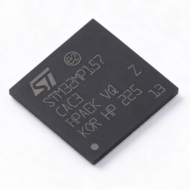
STM32MP157CAC3 - Dual Cortex-A7 650MHz + M4 MPU | ST
The STMicroelectronics STM32MP157CAC3 is a heterogeneous microprocessor (MPU) combining dual Arm Cortex-A7 application cores at 650 MHz with a Cortex-M4 real-time coprocessor at 209 MHz, housed in a 361-ball TFBGA package (12x12 mm per DigiKey listing) rated -40C to +125C. An MPU (microprocessor unit) is a general-purpose processor that runs rich operating systems such as Linux or Android, unlike a microcontroller (MCU) that executes bare-metal or RTOS firmware from on-chip flash. The STM32MP1 series bridges both worlds: the Cortex-A7 subsystem handles Linux-based user interfaces and networking, while the Cortex-M4 core delivers deterministic real-time control, all on one die. This heterogeneous architecture reduces system complexity and BOM cost compared with a discrete MPU-plus-MCU two-chip solution. Key features include 2x Ethernet GMAC with 1-Gbps RGMII compliance per IEEE-802.3ab, 2x USB 2.0 OTG, 8x UART, 5x I2C, 5x SPI, 2x CAN FD, an OpenGL ES 2.0-capable 3D GPU, MIPI DSI display interface, and a 12-bit ADC with up to 16 channels. Memory support spans 16-bit DDR3/DDR3L/LPDDR2/LPDDR3 plus NAND, NOR, and SRAM controllers. A cryptographic accelerator covers AES, DES, 3DES, SHA-1, SHA-256, and MD5 with secure boot support. The device is fabricated on a 28nm FD-SOI process, delivering roughly 1300 DMIPS from the dual Cortex-A7 cores plus 240 DMIPS from the Cortex-M4, with multiple low-power modes (Sleep, Stop, Standby). Core voltage is 1.2 V with I/O rails from 1.8 V to 3.3 V. Typical applications include industrial HMI panels, smart home and IoT gateways, medical monitoring devices, and edge nodes needing Linux connectivity alongside hard real-time motor control or sensor acquisition on the M4 core. Design consideration: use the STPMIC1 PMIC for the required multi-rail power sequencing (VDD, VDD_CPU, VDD_IO) and apply impedance-controlled DDR3 routing with proper termination for signal integrity. This page synthesizes distributor pricing, drop-in same-family alternatives, and practical design notes not found in the manufacturer datasheet.
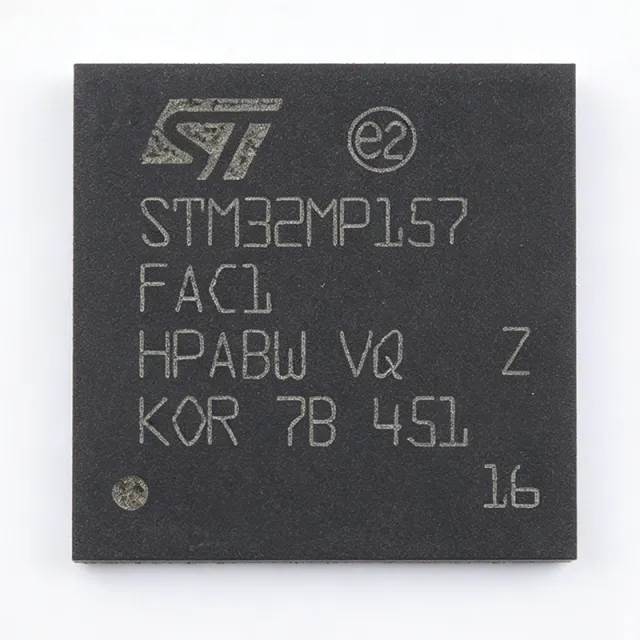
STM32MP157FAC1 - Dual Cortex-A7 + M4 MPU | STMicroelectronics
The STMicroelectronics STM32MP157FAC1 is a high-performance heterogeneous microprocessor (MPU) that combines a dual-core Arm Cortex-A7 application processor running up to 800 MHz with a Cortex-M4 real-time core running up to 209 MHz. This device is designed for advanced embedded applications requiring both rich operating system support (Linux, Android) and deterministic real-time control. It is housed in a 361-ball TFBGA package (12x12 mm, 0.5 mm pitch) and operates over a temperature range of -20°C to +105°C. A microprocessor (MPU) is a complete processing unit that integrates one or more CPU cores, memory controllers, and peripheral interfaces on a single chip, designed to run complex operating systems. In the system hierarchy, an MPU sits above a microcontroller (MCU) in processing power and memory capability, enabling applications such as human-machine interfaces (HMI), industrial gateways, and edge computing. The STM32MP157FAC1 belongs to the STM32MP1 series, which bridges the gap between high-performance application processors and the extensive STM32 ecosystem. Key features include a rich set of connectivity options: 2x Ethernet (10/100/1000 Mbps), 2x USB 2.0 OTG, 8x UART, 5x I2C, 5x SPI, and 2x CAN FD. It also integrates a 3D GPU (OpenGL ES 2.0), a 2D graphics accelerator, and a MIPI-DSI display interface, making it ideal for graphical user interfaces. The device supports up to 1 GB of external DDR3/DDR3L/LPDDR2/LPDDR3 memory and includes a comprehensive security suite with cryptographic acceleration and secure boot. From a technical architecture perspective, the STM32MP157FAC1 uses a heterogeneous multicore design where the Cortex-A7 cores handle high-level operating systems and the Cortex-M4 core manages real-time tasks. The two domains communicate through a hardware mailbox and shared memory, enabling efficient collaboration. The device also features a dedicated power management unit with multiple low-power modes, including standby and shutdown, to optimize energy consumption in battery-powered applications. Typical applications include industrial HMI panels, smart home gateways, medical monitoring devices, and edge AI inference nodes. The combination of high-performance processing, rich graphics, and real-time control makes it a versatile choice for products that require both user interaction and deterministic response. When designing with this device, careful attention must be paid to power sequencing and decoupling. The multiple power rails (VDD, VDD_IO, VDD_3V3, etc.) require proper sequencing to avoid latch-up. A dedicated PMIC (such as the STPMIC1) is recommended to manage the complex power requirements. Additionally, the DDR memory interface requires impedance-controlled routing and proper termination for signal integrity at high speeds.