Produits (44 000+)

HMCAD5831LP9BE - 26 GS/s 3-Bit ADC w/DEMUX | Analog Devices
HMCAD5831LP9BE

HMCAD5831LP9BE - 26 GS/s 3-Bit ADC w/DEMUX | Analog Devices

The Analog Devices HMCAD5831LP9BE is a wideband 3-bit analog-to-digital converter with over/under range bit, sampling at typical speeds of up to 26 GSPS under typical conditions with a Nyquist input. The converter integrates a 1:2 demultiplexer that produces a half-rate clock output, with binary-weighted output bits in which X2 and Y2 serve as the MSBs. Packaged in a RoHS-compliant 64-pin 9 × 9 mm SMT module, the device targets high-speed instrumentation, radar, and wideband digital oscilloscope front-end applications where low-latency, multi-GSPS flash conversion is required. A flash ADC is the highest-speed ADC architecture, in which 2^N parallel comparators simultaneously quantize the input against a resistor ladder reference. The 3-bit flash core delivers one quantization step every clock cycle, with no pipeline latency - critical for time-interleaved measurement systems, pulse-mode radar receivers, and single-shot transient capture. The HMCAD5831 belongs to the wider analog-to-digital converter family, which sits hierarchically under data converters -> mixed-signal ICs -> semiconductors. Key features of the HMCAD5831LP9BE include a wide analog input bandwidth suitable for direct RF sampling, an external reference ladder whose top and bottom voltages are set by the user to customize input common-mode and swing levels, and a Data Inhibit function that forces ADC outputs to zero for test and synchronization. The device operates from -5V and -3.3V supplies, accepts a single-ended AC- or DC-coupled RF input, and demultiplexes its 1:2 output stream at half the sample clock rate. Architecturally, the part uses a fully-parallel comparator array with internal Gray/binary decoding. User-programmable reference ladder voltages allow direct interface to AC-coupled RF front ends or DC-coupled baseband signals without a separate driver amplifier. The half-rate clock output simplifies synchronization with downstream FPGAs or serializer ASICs. Typical applications include wideband radar pulse digitization, digital oscilloscope acquisition front-ends, direct RF sampling in software-defined radio receivers, and high-energy physics instrumentation. It also suits time-domain reflectometry (TDR) and any system requiring a 3-bit flash quantizer with demuxed LVDS-like outputs. When designing with this part, carefully control the reference ladder top/bottom voltages to set the input common mode and full-scale swing for your signal chain. Maintain clean -5V and -3.3V supplies with low-inductance decoupling because the 26 GSPS comparator array draws large transient currents at each clock edge.

Devis Contact
HMCG78CGBSA095N - 16GB DDR5-5600 SODIMM 1Rx8 | SK hynix
HMCG78CGBSA095N

HMCG78CGBSA095N - 16GB DDR5-5600 SODIMM 1Rx8 | SK hynix

The SK hynix HMCG78CGBSA095N is a 16GB DDR5 SODIMM memory module operating at 5600 MT/s (PC5-44800), with CL46 latency at 1.1 V, built on a 1Rx8 organization in a 262-pin unbuffered non-ECC SODIMM package. It uses eight 2Gx8 DDR5 DRAM components (8C configuration) validated to the DDR5-5600B speed bin. A SODIMM (Small Outline Dual In-line Memory Module) is a compact memory module form factor designed for space-constrained systems such as laptops, mini PCs, and embedded platforms. Within the memory hierarchy, it belongs to the DDR5 DRAM module family - the successor to DDR4 - delivering double the bank groups, on-module power management, and higher data rates than the 3200 Mbps typical of DDR4 SODIMMs. Key features of the HMCG78CGBSA095N include the DDR5-5600 data rate per the JEDEC DDR5 standard, PC5-44800 bandwidth class, and a CAS latency of 46 at 1.1 V operation. The 1Rx8 single-rank organization simplifies memory controller training and can reduce power draw compared to dual-rank configurations of the same capacity. Technical architecture: the module integrates eight 2Gb x8 DDR5 SDRAM die per the 8C stacking scheme, an on-module 5V-to-1.1V PMIC (Power Management IC) that moves voltage regulation off the motherboard, and an SPD hub that stores training data and serial presence detect information for the host BIOS. Typical applications include laptop and notebook memory upgrades, mini PC and small-form-factor desktops, industrial computing platforms, and test equipment requiring 16GB of DDR5 SODIMM memory with 5600 MT/s throughput. Design consideration: verify host-platform support for DDR5-5600 SODIMMs and ensure BIOS/SPD compatibility before deployment; mixing modules of different ranks or speed bins may force downclocking to the lowest common denominator. This page synthesizes distributor availability, drop-in same-footprint alternatives, and practical upgrade guidance not found on a single manufacturer page. Pricing and stock data reflect distributor listings as of 2026-09-05.

Devis Contact
HMCG78MEBRA113N - 16GB DDR5-4800 ECC RDIMM | SK hynix
HMCG78MEBRA113N

HMCG78MEBRA113N - 16GB DDR5-4800 ECC RDIMM | SK hynix

The SK hynix HMCG78MEBRA113N is a 16GB DDR5 ECC Registered DIMM (RDIMM) memory module operating at 4800 MT/s (PC5-38400) with CL40 latency at 1.1V, in a 288-pin DIMM form factor with a 1Rx8 (single rank, x8) organization. A registered (buffered) DIMM is a server-class memory module that places a register between the DRAM arrays and the memory controller, reducing electrical load on the command/address lines and enabling higher module counts per channel than unbuffered desktop UDIMMs. RDIMMs sit within the memory module hierarchy (DRAM IC -> module -> registered DIMM -> enterprise memory subsystem) and are the standard memory type for servers and workstations, distinguishing them from unregistered ECC SODIMMs and consumer UDIMMs. Key features of the HMCG78MEBRA113N include its 16GB capacity per module, 4800 MT/s data rate certified as PC5-38400, and on-module ECC registered architecture that corrects single-bit memory errors for data integrity in always-on enterprise systems. The 1.1V operating voltage follows the JEDEC DDR5 standard, delivering lower power per bit transferred than DDR4 RDIMMs of equivalent capacity. The 1Rx8 single-rank organization keeps command scheduling simple for the memory controller and suits dense multi-DIMM-per-channel server boards. Technically, the module uses DDR5 DRAM devices with on-die ECC and a side-band management interface, and the register/buffer logic decouples command/address signaling so the module meets JEDEC DDR5 RDIMM timing at 4800 MT/s with CL40 (40-40-40 typical JEDEC scaling). Backward compatibility to 4400 MT/s is supported on platforms whose memory controllers negotiate lower speeds. Typical applications include enterprise servers based on Intel Xeon Scalable 4th/5th Gen and AMD EPYC processors, such as HPE ProLiant Gen10+/Gen11, Dell PowerEdge 16G series, and Lenovo ThinkSystem platforms, as well as virtualization hosts and data-intensive workloads where ECC protection is mandatory. When designing or configuring systems, populate DIMM slots per the server vendor's population rules for single-rank RDIMMs and confirm that the platform BIOS supports 4800 MT/s; otherwise the module will downclock gracefully to the highest mutually supported JEDEC speed. This page synthesizes distributor pricing, stock data, drop-in alternative module numbers, and platform compatibility notes not found in a single manufacturer datasheet.

Devis Contact
HMCG84AEBRA - 32GB DDR5 4800 RDIMM 1Rx4 ECC Reg | SK hynix
HMCG84AEBRA

HMCG84AEBRA - 32GB DDR5 4800 RDIMM 1Rx4 ECC Reg | SK hynix

The SK hynix HMCG84AEBRA is a 32 GB DDR5-4800 Registered ECC DIMM module in a 288-pin EC8 RDIMM form factor, organized as a single-rank 1Rx4 configuration and operating at the JEDEC-standard 1.1 V supply rail. It delivers a peak data rate of 4800 MT/s (PC5-38400), making it one of the baseline-speed modules in the SK hynix server-memory lineup designed for Intel Sapphire Rapids / 4th Gen Xeon Scalable and AMD EPYC 9004 (Genoa) platforms. A single 32 GB module per channel enables dense memory configurations for virtualization, in-memory databases, and AI inference hosts. A Registered DIMM (RDIMM) is a type of server-class memory module that places a register buffer between the DRAM chips and the memory controller, electrically isolating the controller from the heavy capacitive load of multiple ranks. RDIMMs sit in the memory module hierarchy alongside UDIMMs (unbuffered), LRDIMMs (load-reduced), and MRDIMMs (multiplexed rank), and are the workhorse module type for mainstream dual-socket servers. The 1Rx4 organization means all DRAM chips reside on a single rank accessed across a 64-bit data width split into four x4 devices, which trades peak bandwidth per access for higher module density at lower cost-per-bit. Key features of the HMCG84AEBRA include JEDEC DDR5-4800 conformance, on-module ECC (error-correcting code) for single-bit error correction and multi-bit error detection, on-board voltage regulation via the 12 V PMIC, and the SK hynix 1ynm-class DRAM die. The module carries server-grade validation against common server CPU memory reference designs and supports the standard server thermal envelope of 0–95 °C operating temperature. Typical applications of the HMCG84AEBRA include dual-socket mainstream servers, virtualization hosts running VMware ESXi / Hyper-V / KVM, in-memory databases such as SAP HANA and Redis Enterprise, deep-learning inference nodes, and edge / HPC compute nodes. It is also used as the baseline DDR5-4800 building block for customers who plan to upgrade to higher-speed 5600 MT/s modules later. When designing with this module, follow the server OEM's Qualified Vendor List (QVL) for the exact platform — many OEM servers validate only specific SPD programming revisions (HMCG84AEBRA vs HMCG84AEBRA115N vs HMCG84MEBRA). Mixing 1Rx4 and 2Rx4 modules in the same channel is allowed only in some platforms; consult the BIOS release notes. This page synthesizes distributor pricing, module-revision cross-references, and platform compatibility notes not collated in a single SK hynix product folder.

Devis Contact
HMCG84AHBRA - 32GB DDR5-6400 ECC RDIMM 1Rx4 1.1V | SK Hynix
HMCG84AHBRA

HMCG84AHBRA - 32GB DDR5-6400 ECC RDIMM 1Rx4 1.1V | SK Hynix

The SK Hynix HMCG84AHBRA is a 32 GB DDR5-6400 ECC Registered DIMM (RDIMM) organized as 1Rx4 (single-rank, x4 data width) and operating at 1.1 V with a JEDEC-standard CAS Latency of CL52. Housed on a 288-pin DIMM module, it delivers a peak transfer rate of 6400 MT/s (PC5-51200) suitable for mainstream server, edge compute, and single-socket to dual-socket general-purpose workloads. A DDR5 RDIMM (Registered DIMM) is a server-class memory module that buffers the command, address, and control signals through a register clock driver (RCD) on the module itself, enabling higher densities, better signal integrity at high speeds, and larger channel capacities than unbuffered DIMMs. Within the memory hierarchy, DDR5 sits at the top of the system memory tier - below the CPU cache and above storage (SSDs/HDDs), part of the broader DRAM family under the volatile semiconductor memory category. Key features of the HMCG84AHBRA include 32 GB module capacity, 1Rx4 rank/organization, ECC support for single-bit error correction and multi-bit error detection, on-module voltage regulation (DDR5 PMIC), and a 1.1 V operating voltage that improves performance-per-watt versus DDR4. The PC5-51200 bandwidth and 6400 MT/s data rate enable modern server CPUs to feed multi-core workloads without becoming memory-bound, while 1Rx4 topology supports platforms that prefer single-rank modules for compatibility or specific rank-interleaving schemes. Technically, the module complies with the DDR5 RDIMM standard, integrating an on-board PMIC for voltage regulation, a temperature sensor for thermal management, and ECC (error-correcting code) capability via the JEDEC-defined DRAM features. The x4 organization indicates four-bit-wide DRAM devices on the module, which provides a balance of capacity, parallelism, and error-detection granularity commonly used in server workloads. Typical applications include 1P/2P server platforms running virtualization, enterprise databases, edge compute nodes, low-VM-density compute hosts, AI inference at the edge, and general-purpose data-center workloads where 32 GB per module is the sweet spot for cost-per-gigabyte. It is also used in workstation-class systems requiring ECC memory reliability. When designing or qualifying with HMCG84AHBRA, verify the CPU memory controller's supported DIMM population rules and DDR5-6400 speed bin (some platforms require BIOS updates to enable 6400 MT/s, and 1Rx4 may not be supported on all channels). Always match module ranks per channel per the OEM's memory population guide to avoid downclocking. This page synthesizes distributor pricing snapshots from multiple vendors, JEDEC-compliant drop-in equivalent RDIMMs from competing DRAM manufacturers, and practical population/qualification notes - information not consolidated on the manufacturer product page.

Devis Contact
HT45F0074A - Half-Bridge Induction Cooker Flash MCU | Holtek
HT45F0074A

HT45F0074A - Half-Bridge Induction Cooker Flash MCU | Holtek

The Holtek HT45F0074A is a Flash Memory type 8-bit high-performance RISC architecture microcontroller specially designed for half-bridge induction cooker applications, delivered in a 24-pin SOP (24SOP) surface-mount package. It integrates complementary PWM outputs with adjustable dead-time insertion, an 11-channel 12-bit A/D converter with 2-channel automatic conversion, SPI/I2C/UART serial interfaces, nine groups of over-voltage protection, and a programmable-gain internal operational amplifier. An induction cooker control MCU is an application-specific standard product (ASSP) that sits at the top of the power-appliance control hierarchy: below general-purpose 8-bit MCUs, it adds dedicated analog front-ends and power-control state machines so a single chip can manage resonant half-bridge power stages, user interfaces, and safety monitoring without external comparators or amplifiers. Key differentiating features include the complete hardware protection mechanism covering over-current, surge, and phase-loss conditions, nine programmable over-voltage protection groups (upgraded from seven in the earlier HT45F0074), and complementary PWM outputs with hardware dead-time insertion that directly drive half-bridge gate control. The 12-bit ADC with 2-channel automatic conversion mode continuously samples current and voltage feedback without CPU intervention, freeing processing bandwidth for control loops and user interface tasks. Architecturally, the device uses Holtek's high-performance 8-bit RISC core with Flash program memory, combining fast instruction execution with in-system reprogrammability for production flexibility. The integrated programmable-gain operational amplifier conditions current-sense signals internally, reducing external component count and board area in cost-sensitive appliance designs. Typical applications include 3500W-class half-bridge induction cooker main control (Holtek's official reference design uses this exact chip), other resonant power-control appliances, and induction heating systems requiring hardware-level protection. The SPI/I2C/UART interfaces support display panels, touch keys, and external EEPROM. Design consideration: because the HT45F0074A has been placed on End-of-Life (latest purchase date May 24, 2026, per Holtek EOL notification), new designs should evaluate the Holtek-designated replacement device or design in the HT45F0074 only for service continuity. This page synthesizes verified web data, the Holtek EOL cross-reference, and drop-in alternative analysis not found on the manufacturer product page.

Devis Contact
HT45F8640 - 8-bit BMS Flash MCU, 3-7 Cell Li-ion | Holtek
HT45F8640

HT45F8640 - 8-bit BMS Flash MCU, 3-7 Cell Li-ion | Holtek

The Holtek Semiconductor HT45F8640 is an 8-bit Flash A/D type BMS (Battery Management System) microcontroller with an integrated accumulative cell voltage monitor module, designed specifically for 3 to 7 cell Li-ion rechargeable battery protection applications. It supports a maximum input voltage of 36V, integrates 4KB of Flash program memory and 256B of RAM data memory, and is housed in a 28-pin SSOP-A package. A BMS microcontroller is a specialized type of 8-bit microcontroller unit within the power management IC hierarchy, combining an MCU core with dedicated battery-monitoring analog front-end circuitry. Unlike general-purpose MCUs, BMS devices such as the HT45F8640 integrate cell voltage monitoring, protection FET gate drivers, and high-voltage tolerant front ends, reducing external component count in battery pack designs. Key features include the accumulative cell voltage monitor, which measures an accumulative voltage from cell 1 to cell N and outputs a divide-by-N voltage through an analog multiplexer with ±0.5% accuracy. Integrated discharge and charge N-type MOSFET gate drivers eliminate external gate-drive ICs, while a high accuracy voltage regulator powers the core from the high-voltage pack rail. The device also provides a multi-channel ADC (up to 5 channels) and true EEPROM for storing calibration data and serial numbers. Architecturally, the HT45F8640 is based on Holtek's high-performance 8-bit RISC core with Flash multi-programming capability, enabling field firmware updates. The dedicated analog modules are tightly coupled to the core, allowing fast protection loops for overcharge and overdischarge conditions. Typical applications include 3S to 7S Li-ion battery packs for power tools, e-bikes, portable medical devices, and backup power systems, where integrated cell monitoring and FET drive reduce BOM cost. Design consideration: plan your end-of-life strategy now - Holtek has issued a formal EOL notification for the HT45F8640/HT45F8650, with the last purchase date of October 07, 2026. This page synthesizes the EOL notification, drop-in family alternatives, and design guidance not found on standard distributor pages.

Devis Contact
HT45F8650 - 8-Bit Li-Battery Protection Flash MCU | Holtek
HT45F8650

HT45F8650 - 8-Bit Li-Battery Protection Flash MCU | Holtek

The Holtek Semiconductor HT45F8650 is an 8-bit BMS (Battery Management System) Flash microcontroller with an integrated accumulative cell voltage monitor, designed specifically for 3 to 8 cell Li-ion rechargeable battery protection in a 48-pin LQFP-EP package. It integrates a multi-channel 12-bit A/D converter, a comparator, a high-accuracy voltage regulator, and dedicated Li-ion battery protection functions including two discharge N-type MOSFET gate drivers and one charge N-type MOSFET gate driver. A battery management MCU is a class of embedded controller that combines battery-specific analog front-end functions with a general-purpose processor core, sitting within the hierarchy of 8-bit Flash MCUs used in power management and battery protection integrated circuits. The accumulative cell voltage monitor outputs a divide-by-N voltage of the stacked cells to the analog multiplexer with a ±0.5% divided ratio accuracy, which is then digitized by the internal 12-bit ADC. Key features include up to 36V maximum input voltage tolerance, 8KB of Flash program memory, 512 bytes of RAM data memory, and True EEPROM for storing serial numbers and calibration data. Flash multiple-program capability simplifies firmware iteration, while the integrated MOSFET gate drivers eliminate external driver ICs and reduce bill-of-materials cost. Architecturally, the device uses Holtek's high-performance 8-bit RISC core with multiple flexible Timer Modules providing timing, pulse generation, and PWM output functions. Complete SPI, I2C, and UART interfaces allow straightforward communication with external hardware such as fuel gauges, displays, or host controllers. Typical applications include handheld measurement instruments, electric power tools, handheld hair dryers, and handheld vacuum cleaners - portable battery-powered products where accurate cell monitoring and reliable charge/discharge protection are mandatory safety requirements. A key design consideration is that the OCP (over-current protection) circuit power source can be selected between a general I/O pin and VDD (5V); pins such as PA0 and PA3 may host two coexisting functions but cannot use both simultaneously, so pin assignment must be planned early. This page synthesizes verified datasheet excerpts, distributor pricing context, same-family drop-in options, and practical BMS design notes not found together on the manufacturer site.

Devis Contact
HT66F25D - A/D Flash 8-bit MCU with EEPROM | Holtek
HT66F25D

HT66F25D - A/D Flash 8-bit MCU with EEPROM | Holtek

The Holtek HT66F25D is an A/D Flash type 8-bit MCU with EEPROM, built on a high-performance RISC architecture, supplied in an SOP small-outline package. It belongs to Holtek's enhanced Flash MCU family that integrates an analog-to-digital converter, non-volatile EEPROM data memory, and a high-current LED driver output structure on a single chip, allowing multi-programming convenience thanks to its Flash program memory. An 8-bit Flash microcontroller is a complete computing system on a single integrated circuit: it combines a processor core, program Flash memory, data RAM, EEPROM, peripheral functions such as timers, PWM and ADC channels, and general-purpose I/O. Within the semiconductor hierarchy, the HT66F25D sits in the microcontroller -> embedded processor -> integrated circuit taxonomy, positioned for cost-sensitive embedded control where on-chip analog input and small non-volatile data storage remove the need for external components. Key differentiating features of this device, as stated by Holtek and the datasheet aggregators carrying the official document, include the Flash program memory with multi-programming support (enabling in-circuit update during development and production), the integrated A/D converter for reading analog sensors directly, the on-chip EEPROM for calibration data and user settings that must survive power cycles, and the enhanced high-current LED driver capability highlighted in Holtek's product notification for the HT66F24D/HT66F25D family. Architecturally, the device follows Holtek's RISC-style 8-bit core used across the HT66Fx1D series, with register-mapped I/O ports (PA, PB, PC with individual pull-up and wake-up control bits per the datasheet register lists), typical of the family's low-cost, low-pin-count embedded control philosophy. The exact clock frequency range, ADC resolution, Flash and RAM capacities are detailed in the 175-page official datasheet and should be confirmed there for each specific suffix. Typical applications include small appliance control, LED lighting and brightness control exploiting the high-current driver outputs, battery chargers, sensor interfaces using the A/D converter, and consumer products requiring configuration storage in EEPROM. A key design consideration: this device has been formally phased out by Holtek. According to the official Holtek EOL notification PDF, the last time buy date was April 14, 2026, so new designs must qualify a replacement immediately. This page synthesizes distributor sourcing data, the official Holtek EOL cross-reference notice, and drop-in replacement analysis not found on standard datasheet aggregator sites.

Devis Contact
HT66FB550 - 8-bit USB Flash MCU, 8KB, LQFP-48 | Holtek
HT66FB550

HT66FB550 - 8-bit USB Flash MCU, 8KB, LQFP-48 | Holtek

The Holtek Semiconductor HT66FB550 is an 8-bit Flash A/D USB microcontroller with a 12-bit ADC, 8KB of Flash program memory, 37 general-purpose I/O lines, an SPI interface, and USB 2.0 Full Speed connectivity, housed in a 48-pin LQFP (7x7 mm) package. An 8-bit microcontroller unit (MCU) is a single-chip computer that integrates a processor core, memory, and peripherals on one die, sitting within the broader hierarchy of semiconductor devices as: microcontroller -> embedded processor -> integrated circuit. The HT66FB550 belongs to Holtek's A/D Flash USB series, which combines Holtek's high-performance RISC core with direct analog signal interfacing and a USB interface, eliminating the need for a separate USB transceiver chip in many designs. Key features include the USB 2.0 Full Speed device controller (12 Mbps), a 12-bit resolution analog-to-digital converter, 8KB of Flash program memory, an SPI serial interface, and a wide operating voltage range of 2.2V to 5.5V. These specifications make the device well suited to cost-sensitive designs that must digitize analog sensor signals and stream them over USB without a discrete USB bridge. Technically, the HT66FB550 uses Holtek's 8-bit high-performance RISC architecture, common to the HT66FB540, HT66FB550, and HT66FB560 family members, which differ mainly in memory density and pin count. The integrated USB serial interface engine (SIE) handles protocol framing in hardware, reducing firmware overhead and CPU loading compared with bit-banged USB implementations. Typical applications include USB HID devices such as game controllers and keyboards, USB sensor data loggers, battery chargers with USB telemetry, test fixtures, and industrial control panels that interface directly to analog transducers through the 12-bit ADC. When designing with this device, respect the 2.2V to 5.5V supply range and place 0.1uF decoupling capacitors at each VDD pin; the USB full-speed line requires 22-ohm series resistors and careful 90-ohm differential routing on the DP/DM pair. This page synthesizes distributor pricing, drop-in family alternatives, application guidance, and design notes not found in the manufacturer datasheet, offering engineering value beyond a raw specification listing.

Devis Contact
ICE40HX4K-TQ144 - 3520-LUT 1.2V FPGA | Lattice Semiconductor
ICE40HX4K-TQ144

ICE40HX4K-TQ144 - 3520-LUT 1.2V FPGA | Lattice Semiconductor

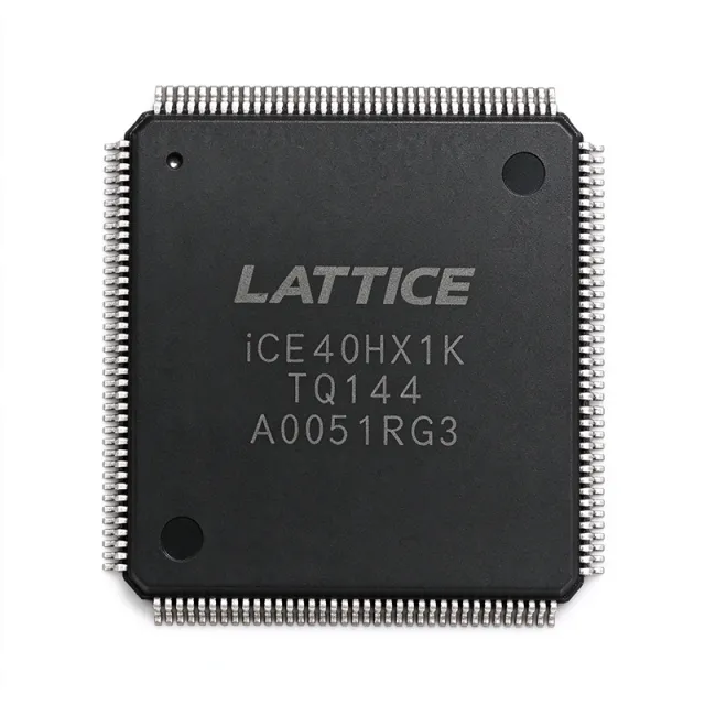
The Lattice Semiconductor ICE40HX4K-TQ144 is an ultra-low-power HX-series field-programmable gate array (FPGA) with 3,520 logic cells, 107 I/Os, 81,920 bits of configuration memory, and a 144-pin TQFP package. It operates from a 1.2 V core supply according to the supplied distributor data. The device targets compact, low-power programmable logic systems where FPGA flexibility is needed without the power and board complexity of a larger high-performance FPGA. A field-programmable gate array is a configurable digital semiconductor that contains programmable logic blocks, routing resources, input/output blocks, and configuration memory. In the hierarchy, an FPGA is a programmable logic device, a digital IC, and a semiconductor. Unlike a fixed-function microcontroller or application-specific integrated circuit, an FPGA can be programmed after manufacture to implement parallel data paths, control logic, serial interfaces, and hardware signal processing. The ICE40HX4K provides 3,520 logic cells and 81,920 bits of configuration memory, as identified by DigiKey and Mouser search results. Its 107 I/Os provide substantial connectivity for external memory, sensors, communications, control signals, and general-purpose digital interfaces. The HX family is positioned by Lattice as a low-power, high-performance FPGA family, making the part suitable for embedded control, communication, instrumentation, and education platforms where low static power and fast programmable logic are important. The 144-pin TQFP package exposes the FPGA in a conventional surface-mount form factor suitable for automated assembly and multilayer PCB designs. The verified source snippets identify the package as 144-pin TQFP or 144-LQFP terminology; designers should confirm the exact mechanical drawing and pin names against the manufacturer datasheet before releasing a PCB footprint. The supplied data does not specify speed grade, temperature range, power consumption, pin names, memory architecture beyond configuration capacity, or I/O voltage limits. Typical uses include custom interface controllers, low-power sensor aggregation, digital signal conditioning, communications adapters, test fixtures, and FPGA-based education or prototyping boards. For a new design, use the manufacturer’s configuration toolchain and verify pin assignments, supported I/O standards, clocking resources, power rails, decoupling requirements, and programming interface compatibility. Because the supplied evidence confirms the family and capacity but not a complete electrical characterization, unsupported values should not be inferred from generic iCE40 family claims.

USD $10,66 En stock
ICL7106CJL - 3.5-Digit LCD ADC | Analog Devices
ICL7106CJL

ICL7106CJL - 3.5-Digit LCD ADC | Analog Devices

The Analog Devices ICL7106CJL is a production 3.5-digit successive-approximation analog-to-digital converter with direct LCD display drivers, supplied in a 40-pin ceramic dual-inline package. It combines a multiplexed seven-segment LCD output with an integrated analog measurement system designed for panel meters, laboratory instruments, and industrial transducers. The original device family was also associated with Harris, Intersil, and Maxim Integrated, while the current manufacturer product page identifies the ICL7106 as a production part. An integrated data converter is a mixed-signal semiconductor that converts an analog input voltage into a numeric representation. In the ICL7106, the converter and LCD-driving functions are combined to reduce the number of external components required for a digital panel display. Analog Devices describes the device family as a 3.5-digit A/D converter with direct LCD drivers, allowing the measured result to be displayed without a separate display-driver IC in conventional applications. The converter's defining application feature is its direct seven-segment LCD drive capability. The measured count is represented as a three-digit display plus sign or other status information, depending on the external circuit configuration. The 40-pin CDIP construction also provides ample connection count for analog inputs, references, oscillator components, display outputs, and control functions described in the manufacturer documentation. The ICL7106 family uses a dual-slope conversion technique, which is useful when rejecting interference at frequencies related to the integration period. Analog Devices states that dual-slope conversion automatically rejects interference signals common in industrial environments. The same product overview identifies true differential input and reference capability as useful for ratiometric measurements involving ohms, resistive bridges, and bridge transducers. Typical uses include digital panel meters, laboratory meters, process-control displays, temperature indicators, weighing systems, and other equipment that must measure an analog quantity and present it locally on an LCD. A panel-meter design can place the ICL7106 close to the sensor interface, route the analog input and reference through short paths, and connect the display directly to the converter's LCD outputs. When laying out an ICL7106CJL circuit, follow the pin-description and typical-application diagrams in the manufacturer datasheet for input filtering, reference routing, oscillator components, and LCD connections. Keep sensitive analog and reference nets away from display outputs and switching nodes. Because the CDIP package is through-hole, its long leads make hand insertion straightforward, but production designs must still account for lead spacing, board cleanliness, and mechanical strain. This product record combines the manufacturer overview, distributor identification of the 40-CDIP package, lifecycle information, and cross-reference findings for ICL7106CJL. It also distinguishes directly documented characteristics from fields that require confirmation against the datasheet, helping engineers plan replacement sourcing without relying on unverified electrical assumptions.

Devis Contact
ICL7106CPL+ - 3.5-Digit LCD ADC | Analog Devices
ICL7106CPL+

ICL7106CPL+ - 3.5-Digit LCD ADC | Analog Devices

Analog Devices ICL7106CPL+ is a low-power, 3.5-digit monolithic analog-to-digital converter with a 40-pin PDIP package. It integrates a seven-segment decoder, LCD display driver, voltage reference, and clock circuit, allowing a measurement system to display the converted result without external display-drive circuitry. The verified product information identifies the converter as a high-performance, low-power device intended for liquid-crystal display instruments. An A/D converter transforms an analog input voltage into a numeric representation. The ICL7106 integrates the functions needed for a basic digital panel meter: input conditioning, conversion, seven-segment decoding, polarity indication, display drivers, an internal reference, and an oscillator. In the electronic-component hierarchy, it is an ADC, a data-conversion IC, and a mixed-signal instrument integrated circuit. It differs from the ICL7107 because the ICL7106 includes multiplexed backplane drive for an LCD rather than direct drive for a larger LED display. The verified sources describe the ICL7106 as a high-performance, low-power 3.5-digit converter with very high input impedance. On-chip active components include polarity and digit drivers, segment decoders, a voltage reference, and a clock circuit. These integrated functions reduce the number of external components required in a panel-meter design while providing a direct interface to a nonmultiplexed liquid-crystal display. The C designation and PL package identify a temperature-grade and packaging arrangement within the ICL7106 product family, while the trailing plus denotes the lead-free ordering code used by current distributor records. The device is supplied in a 40-pin PDIP package identified by distributor listings as 40-PDIP or 40-DIP. The manufacturer product page lists the ICL7106 as a production 3.5-digit A/D converter and provides its family documentation. Typical uses include digital panel meters, laboratory instruments, temperature indicators, process-monitoring displays, weighing scales, and other instruments that measure an analog voltage and present the result on a seven-segment LCD. Because the converter includes the display decoder and driver, it is especially useful where a compact instrument display is required without building a separate display interface. The principal design consideration is to follow the manufacturer's recommended input, reference, clock, display, and bypass connections. Because the exact pin names, input limits, conversion timing, reference characteristics, and electrical ratings are not included in the supplied excerpts, engineers should verify those values and the complete pinout in the manufacturer datasheet before final PCB or firmware design. This product page consolidates current distributor availability, verified pricing, source links, package information, replacement context, and practical design considerations. It distinguishes the ICL7106's LCD-focused role from the LED-oriented ICL7107 and makes missing technical data explicit rather than estimating values that are not supported by the retrieved sources.

Devis Contact
ICL7106EJL - 3.5-Digit LCD A/D Converter | Maxim Integrated
ICL7106EJL

ICL7106EJL - 3.5-Digit LCD A/D Converter | Maxim Integrated

The Maxim Integrated ICL7106EJL is a low-power, 3.5-digit successive-approximation analog-to-digital converter designed for direct liquid-crystal display interfacing. The device operates from a 15 V supply and is packaged in a 40-pin ceramic dual-inline package, designated CDIP-40. Its integrated signal-conditioning and display features make it suitable for standalone digital instrumentation, panel meters, laboratory equipment, and precision weighing systems. An A/D converter is an interface integrated circuit that converts an analog voltage into a digital value for measurement, display, control, or data processing. The ICL7106EJL belongs to the specialized ADC and DAC product family, combining a 3.5-digit conversion engine, seven-segment decoder, display driver, reference source, clock, and digital filtering. Unlike a general-purpose ADC requiring an external display controller, it is optimized for multiplexed LCD glass. The ICL7106 uses differential input architecture, allowing a measurement amplifier and reference arrangement to reject common-mode voltage. Its integrated reference source simplifies standalone designs, while digital filtering helps stabilize displayed results. The EJL ordering code identifies the 15 V, extended-temperature and CDIP-40 variant associated with this product designation. Typical applications include digital panel meters, laboratory measurement instruments, process-monitoring equipment, temperature controllers, and portable instrumentation. When implementing a circuit, evaluate input overdrive, reference accuracy, LCD segment drive requirements, and the relationship between integration time, noise performance, and conversion speed. The ceramic package also requires attention to thermal dissipation and mechanical handling during soldering and assembly. This product page combines the manufacturer device description with practical application guidance, pin-package information, design considerations, and sourcing support. For current pricing, inventory, lead time, and delivery options, use the Request a Quote form on this page rather than relying on historical distributor figures.

Devis Contact
ICL7106EPL+ - 3.5-Digit LCD ADC | Maxim Integrated
ICL7106EPL+

ICL7106EPL+ - 3.5-Digit LCD ADC | Maxim Integrated

The Maxim Integrated ICL7106EPL+ is a monolithic 3.5-digit analog-to-digital converter designed to measure low-frequency differential or single-ended inputs and drive a nonmultiplexed liquid-crystal display. It integrates a voltage reference, clock circuit, polarity and digit drivers, segment decoders, and the functions required for direct LCD operation. The device is packaged as a 40-pin PDIP, with industrial-temperature ordering indicated by the E suffix. The + suffix identifies the manufacturer's lead-free product designation. The ICL7106 family is intended for instrumentation applications where a dedicated display, digital measurement, and relatively low power are more important than high conversion speed. An analog-to-digital converter, or ADC, converts a continuously varying analog voltage into a numeric value. A 3.5-digit integrating ADC such as the ICL7106 uses an integrating measurement approach and includes display decoding and drive circuitry, reducing the external component count required for a standalone panel meter. The ICL7106 differs from the related ICL7107 by driving a nonmultiplexed LCD, while the ICL7107 is intended for LED-display applications. This distinction makes display type an essential PCB and firmware-independent hardware selection criterion. The principal system-level benefits are integration and measurement simplicity. A high-input-impedance measurement front end allows the converter to work with sensor and instrumentation circuits without adding a separate display driver. On-board segment decoders, polarity and digit drivers, a voltage reference, and a clock eliminate several discrete functions from the meter design. These characteristics are especially useful in standalone laboratory instruments, temperature controllers, weighing indicators, process monitors, and service equipment where the analog input must appear directly as a readable numerical measurement. Because the ICL7106 is intended for low-power measurement rather than high-speed waveform acquisition, system timing and input conditioning determine practical performance. The input network, reference arrangement, integration period, clock source, and bypass components should follow the manufacturer's application guidance. Decoupling must be placed close to the supply and reference pins, while the analog input path should avoid long traces and sources of leakage. The LCD interface and converter functions are integrated, but the display still requires the appropriate glass connections and suitable common and segment drive arrangement. Typical applications include digital panel meters, temperature measurement instruments, laboratory readouts, industrial process indicators, portable measurement equipment, and equipment with an integrated numeric display. In these systems, the ICL7106EPL+ serves as both the measurement engine and the LCD interface. Designers should confirm the input range, reference voltage, conversion timing, display configuration, and supply requirements against the manufacturer datasheet before finalizing the analog front end and printed-circuit-board layout. For PCB design, begin by assigning the 40-pin PDIP footprint and checking the manufacturer's pin-description table for analog inputs, reference connections, supply rails, ground pins, clock connections, and LCD outputs. Avoid routing LCD segment and digit lines next to high-impedance analog inputs. Place input and bypass capacitors close to their associated pins, provide a stable ground return, and keep the analog and display paths physically separated where the board area permits. This product page combines the manufacturer's family-level technical description, package and ordering information, related 40-pin device data, application engineering guidance, and a replacement-focused comparison. It is intended to help engineers determine whether the ICL7106EPL+ matches the required display technology, package, lifecycle requirement, and instrumentation architecture before committing the design to production.

Devis Contact

ICL7106IP - 3.5-Digit LCD A/D Converter | Analog Devices
ICL7106IP

ICL7106IP - 3.5-Digit LCD A/D Converter | Analog Devices

The Analog Devices ICL7106IP is a low-power, 3.5-digit successive-approximation A/D converter with integrated seven-segment decoders, LCD display drivers, reference, and clock circuitry in a 40-pin PDIP package. The converter is designed for liquid-crystal displays and uses dual-slope conversion to provide stable measurements in instrument and industrial environments. An A/D converter is an analog-to-digital converter that transforms a continuously varying voltage or current-derived signal into a numeric representation. The ICL7106 belongs to the display-oriented A/D converter hierarchy, combining measurement conversion, display decoding, display drive, reference voltage, and timing functions in one device. Its integrated LCD backplane drive is intended to reduce the external circuitry required for panel instruments. Key features of the ICL7106 include 3.5-digit resolution, seven-segment display decoding, LCD display-driver capability, an integrated reference, an integrated clock, true differential input and reference support, and dual-slope conversion. The device family is designed to reject interference signals common in industrial environments, while ratiometric measurement support is useful for ohms and bridge-transducer applications. The ICL7106 uses dual-slope conversion rather than a high-speed successive-approximation architecture. This approach integrates an input over a fixed measurement interval and compares the resulting charge with a reference-derived ramp. The architecture is well suited to panel meters, digital scales, temperature indicators, and other systems where measurement rate is less important than stable displayed readings and straightforward system integration. Typical applications include digital panel meters, resistance measurement instruments, bridge-sensor instrumentation, industrial process displays, laboratory meters, weighing systems, and portable measurement equipment. The LCD-focused ICL7106 is generally preferable to LED-display converter variants when the design uses a multiplexed liquid-crystal panel. Designers should follow the manufacturer datasheet for the exact pin assignments, reference connections, clock requirements, display timing, and input common-mode limits. The 40-pin PDIP footprint also requires sufficient board space, careful decoupling, and routing that separates sensitive analog input and reference paths from display-drive and digital timing nodes. This page consolidates manufacturer information, distributor availability, pricing context, package identification, and design guidance for engineers evaluating the ICL7106IP in new or replacement LCD instrument designs.

Devis Contact
ICL7106IPL 3.5-Digit LCD A/D Converter | Maxim
ICL7106IPL

ICL7106IPL 3.5-Digit LCD A/D Converter | Maxim

The Maxim ICL7106IPL is a low-power 3 1/2-digit analog-to-digital converter designed for direct liquid-crystal display interfacing. It integrates the converter, seven-segment decoders, display drivers, voltage reference, and clock circuitry in one device, reducing the external component count required for a standalone measurement instrument. The ICL7106 is associated with the Intersil ICL7106 and ICL7107 family of high-performance, low-power display A/D converters. An ADC converts an analog voltage into a digital numerical representation. In the ICL7106, the conversion result is intended for a multiplexed LCD rather than a directly driven LED instrument display. The integration of the display drivers and reference circuit makes the device suitable for digital panel meters, laboratory instruments, handheld meters, weighing systems, and other equipment where a stable numeric readout is required. The principal function of the ICL7106IPL is measurement conversion combined with display control. Its 3 1/2-digit format is designed for applications where a signed or otherwise bounded numerical range is sufficient. The device includes polarity and digit drivers, segment decoders, a voltage reference, and a clock circuit, allowing the measurement system to operate without separate display-driver circuitry. The ICL7106 architecture uses a successive integration conversion technique associated with this family of low-power metering ICs. This approach is suited to relatively slow measurements where low power, good linearity, and display integration are more important than high sampling rates. The converter’s high input impedance helps reduce loading of the signal source, while the integrated reference supports repeatable measurement results when paired with appropriate external input, reference, and display networks. The ICL7106 family is commonly associated with digital voltmeters, current meters, panel meters, laboratory measurement equipment, and embedded instrumentation. A typical design provides the analog input to the converter, uses external components to set the measurement range and reference, and connects the converter to a multiplexed LCD. The ICL7106 variant is particularly appropriate when the display is an LCD; ICL7107 is generally identified with LED-display applications. When designing a circuit around ICL7106IPL, verify the package pinout and display interface against the manufacturer datasheet before assigning PCB tracks. Input filtering, reference decoupling, display glass compatibility, and the external component values for range and timing determine practical measurement performance. Because the available manufacturer page confirms the family function but does not state the complete ICL7106IPL electrical limits in the retrieved material, check the current datasheet for operating voltage, conversion timing, input range, and absolute maximum ratings. This product page combines the confirmed ICL7106 family architecture, the available official product-page information, and clearly identified cross-reference candidates. The comparison and selection notes emphasize package and pin compatibility, while the application guidance focuses on practical use of a low-power 3 1/2-digit LCD measurement system.

Devis Contact
ICL7107CDL - 3.5 Digit Display ADC | Harris | 40-SBDIP
ICL7107CDL

ICL7107CDL - 3.5 Digit Display ADC | Harris | 40-SBDIP

Harris Corporation ICL7107CDL is a 3.5-digit CMOS analog-to-digital converter designed for panel-meter and digital-display applications. The device combines a 40-pin SBDIP package with a 6 V supply indication and is specifically associated with LED display drivers. Its measurement architecture is intended to produce stable, readable results from low-level analog inputs while driving multiplexed seven-segment displays. An ADC such as the ICL7107CDL is a mixed-signal integrated circuit that converts an analog voltage into a numeric value. In the broader hierarchy, it belongs to data-converter ICs, analog-to-digital converters, and display-oriented measurement ICs. The ICL7107 family is commonly used where a panel meter, digital voltmeter, counter, or process-monitoring instrument needs to present an electrical measurement directly through a seven-segment display. The key application feature of the ICL7107CDL is its integrated 3.5-digit conversion and display-driver function. A 3.5-digit meter can display a full range of digits plus one sign or half-digit indication, making it suitable for positive or negative measurements. The 40-SBDIP through-hole package supports conventional PCB mounting, socket assembly, and repair or replacement of older instrument designs. The verified product listing identifies the device as a 40-SBDIP Harris Corporation part. The ICL7107CDL is associated with LED display drivers, which makes it appropriate for digital voltmeters, bench instruments, industrial panel meters, laboratory equipment, and embedded measurement panels. Its external connection requirements, reference voltage, input range, timing behavior, and display-drive characteristics must be confirmed against the manufacturer datasheet before a new PCB is laid out. The device should not be selected solely from its display-driver description because sensor excitation, reference accuracy, input filtering, and calibration determine the final measurement performance. For an instrument design, place the converter close enough to the analog input and reference network to minimize pickup on high-impedance nodes. Use a stable reference arrangement, appropriate input filtering, and decoupling near the supply pins. A conventional through-hole layout should preserve the manufacturer's pin numbering and provide adequate board spacing for the 40-pin SBDIP body. Verify the exact display-driver outputs and segment/common-anode or common-cathode requirements against the target display. This product page combines the Harris and Intersil documentation references, verified distributor identification, package information, application positioning, and engineering guidance. It distinguishes the ICL7107CDL from broader cross-reference candidates by focusing on the 40-pin SBDIP footprint and the practical requirements of 3.5-digit panel-meter designs rather than presenting a generic ADC overview.

Devis Contact
ICL7107CMH+ - 3.5-Digit Dual-Slope ADC | Analog Devices
ICL7107CMH+

ICL7107CMH+ - 3.5-Digit Dual-Slope ADC | Analog Devices

The Analog Devices ICL7107CMH+ is a production 3.5-digit dual-slope analog-to-digital converter designed for precision measurement and digital panel-meter applications. It uses a true differential input and differential reference, provides seven-segment LED display outputs, and is packaged in a 44-pin MQFP measuring 10 mm by 10 mm. The converter combines integration-based measurement with LED display drive circuitry in one device. An ADC converts an analog voltage into a numeric value for measurement, control, or display. The ICL7107 belongs to the dual-slope ADC family, where an unknown input voltage is compared with a reference through integrated and de-integrated phases. This measurement technique is especially useful for slow-moving signals from sensors, resistive transducers, and laboratory instruments because its averaging behavior helps reject periodic interference present in industrial environments. Its architecture also supports ratiometric measurements in which the result depends on the ratio of input voltage to reference voltage. The primary features of the ICL7107CMH+ include its 3.5-digit conversion format, dual-slope conversion technique, true differential analog input, true differential reference input, and direct LED display drive. The integrated display outputs reduce the component count required for common digital panel meters. The zero-integrator phase described for the ICL7106 and ICL7107 family allows the integrator to return to a defined state between measurement cycles, supporting repeatable operation in successive conversion cycles. Its operating limits, conversion time, input ranges, and reference requirements must be confirmed from the manufacturer datasheet for the selected system implementation. The ICL7107 is intended for instrumentation rather than high-speed waveform acquisition. Dual-slope conversion prioritizes resolution and rejection of common interference over conversion speed, making it suitable for panel meters, laboratory measurement equipment, process monitoring, weighing systems, and temperature or bridge-based instrumentation. Differential measurement also helps reject common-mode voltage when the source and return paths are arranged carefully, provided the input common-mode range and reference limits are respected. Common implementations place the ICL7107CMH+ between a sensor or bridge and a seven-segment display. The analog input is conditioned before entering the converter, while the reference and common terminals establish the measurement range. External timing, reference, and display components must follow the recommended application circuit. Care is required when routing the analog input and reference nets because long traces and high-impedance nodes can increase noise pickup, and the LED display driver outputs should not be confused with the analog measurement pins. Designers should confirm the exact pin function for every connection using the pin-description table in the Analog Devices datasheet. The 10 mm by 10 mm MQFP footprint requires a land pattern with adequate thermal and solder-joint area, while the analog input and reference routing should be kept away from display-driver and switching-node traces. When replacing another display ADC, verify not only the conversion resolution but also input range, reference topology, display-drive capability, package dimensions, pin assignment, and conversion timing. This page combines the manufacturer product information, package identification, family-level operating characteristics, qualified same-package order variants, and practical implementation guidance. It also highlights the measurements that must be checked before substitution, helping engineers distinguish genuine pin-compatible options from parts that merely share the same conversion category or display function.

Devis Contact
ICL7107CPL+ - 3.5-Digit Display ADC | Maxim Integrated
ICL7107CPL+

ICL7107CPL+ - 3.5-Digit Display ADC | Maxim Integrated

Maxim Integrated ICL7107CPL+ is a monolithic 3.5-digit analog-to-digital converter with an integrated seven-segment decoder, display driver, voltage reference, and clock circuit. It performs approximately 3 samples per second and is specified in a 40-pin PDIP package. The device is designed for direct seven-segment LED display output and provides high input impedance without requiring external display-drive circuitry. An analog-to-digital converter, or ADC, converts an analog input voltage into a digital value that can be processed, displayed, or transmitted. The ICL7107CPL+ belongs to the broader ADC > data-converter > semiconductor hierarchy. Its integrated dual-slope conversion system is intended for instrumentation applications where moderate resolution, low component count, and direct display output are more important than high-speed sampling. The ICL7107CPL+ includes polarity and digit drivers, segment decoders, an internal voltage reference, and a clock circuit. According to the Analog Devices product page, the dual-slope conversion technique automatically rejects interference signals commonly encountered in industrial environments. True differential input and reference connections also support ratiometric measurements such as resistance and bridge-transducer measurements. The ICL7107CPL+ supports approximately 3 samples per second and includes a zero-integrator phase that improves settling behavior. Its integrated display interface reduces the number of external components needed for a complete measurement panel. The 40-pin PDIP package is suitable for through-hole industrial, laboratory, educational, and legacy control equipment where a large DIP footprint and direct LED display connection are practical. Typical uses include digital panel meters, laboratory voltmeters, temperature indicators, process monitoring instruments, and low-speed sensor interfaces. Because the converter is display-oriented rather than a high-speed sampling ADC, it is most appropriate for continuously updated numerical measurements rather than waveform acquisition, communication receivers, or precision automation channels. A successful design must provide suitable input, reference, and supply bypassing while following the manufacturer’s recommended component values and timing arrangement. LED displays impose load-dependent supply current, so the power source and decoupling should be checked at minimum operating voltage and maximum digit current. For a substitute, verify the complete 40-pin assignment, LED versus LCD output type, reference behavior, sampling interval, and timing before approving a drop-in replacement. This page combines the verified product, distributor, and cross-reference information with a drop-in-focused comparison, practical design guidance, and explicit data gaps. It highlights where published sources confirm package and function and where engineers must consult the detailed datasheet before production substitution.

Devis Contact
ICL7109CMH+ - 12-Bit Dual-Slope ADC, 44-MQFP | Maxim Integrated
ICL7109CMH+

ICL7109CMH+ - 12-Bit Dual-Slope ADC, 44-MQFP | Maxim Integrated

The Maxim Integrated ICL7109CMH+ is a 12-bit plus sign, monolithic CMOS dual-slope integrating Analog-to-Digital Converter (ADC) housed in a 44-pin Metric Quad Flat Pack (MQFP) package, commercial temperature grade. It integrates the reference, oscillator, high-accuracy comparator, bypass switches, and I/O latches required for a complete 12-bit ADC, requiring only a handful of external passive components plus an AC reference or crystal to form a full precision conversion system. Differential inputs, true differential reference inputs, and a built-in +5V reference reduce external analog conditioning needs. A dual-slope integrating ADC is a type of data converter that integrates an input voltage over a fixed time, then de-integrates against a known reference and counts clock pulses to derive a digital result. The architecture provides excellent 50 Hz/60 Hz normal-mode rejection, inherent zero-drift, and monotonic 12-bit performance, making this category a workhorse for digital panel meters, weighing scales, and process instrumentation where linearity and noise immunity matter more than throughput. Key features include 12-bit plus sign resolution, true differential inputs, on-chip charge-pump-driven +5V reference, low typically <10 mW power consumption, parallel interface, and a built-in oscillator buffer. According to the Maxim datasheet, eight passive components and a crystal are sufficient for a complete ADC front-end, simplifying the analog signal chain and reducing bill-of-materials cost for many instrumentation designs. Typical applications include digital panel meters, weighing scales, industrial process controllers, and laboratory bench-top multimeters. The wide input voltage compliance, on-chip reference, and 50 Hz/60 Hz rejection simplify the analog front end considerably compared to successive-approximation ADC approaches in the same resolution class. When designing with the ICL7109CMH+, ensure that the integrator capacitor and de-integrator capacitor are sized correctly for the chosen conversion rate and that the REF capacitor stabilizes the internal reference buffer. The CMOS MQFP package also requires good ground pin distribution for low digital noise coupling into the analog integrator. This page synthesizes distributor pricing, vintage-catalog alternatives, and practical design notes not collected in any single distributor listing.

Devis Contact
ICL7109CMH+D - 12-Bit Dual-Slope ADC, 44-MQFP | Maxim Integrated
ICL7109CMH+D

ICL7109CMH+D - 12-Bit Dual-Slope ADC, 44-MQFP | Maxim Integrated

The Maxim Integrated ICL7109CMH+D is a 12-bit plus sign, CMOS low-power, dual-slope integrating analog-to-digital converter (ADC) housed in a 44-pin MQFP (10x10 mm) package. It integrates a precision reference, clock oscillator, and 3-state binary output drivers, requiring only eight passive components plus a crystal to form a complete integrating ADC front-end. An integrating ADC (also called a dual-slope ADC) is a class of analog-to-digital converter that converts an analog input voltage into a digital representation by integrating the input over a fixed time window and then measuring the time required to de-integrate against a known reference. Within the broader ADC taxonomy, the integrating type sits between successive-approximation-register (SAR) ADCs and sigma-delta ADCs; it offers excellent rejection of mains-frequency noise, inherent input integration (noise averaging), and differential input capability, at the cost of lower conversion rate (typically a few conversions per second to a few hundred). The ICL7109 delivers ±0.5 LSB (typical) integral non-linearity, on-chip differential input stage accepting ±4.2V common-mode range, true differential inputs and differential reference, and TTL-compatible 3-state outputs that interface directly to microprocessors. The part operates from ±5V supplies, consumes under 30 mW, and provides a BYTE/HBENA strobe for simplified 8-bit bus interface. Typical applications include digital panel meters, digital multimeters (DMMs), process controllers, weigh scales, and any precision low-frequency measurement where 50 Hz/60 Hz normal-mode rejection and differential inputs are critical. Its differential reference input also enables ratiometric measurement such as bridge-style transducers. When designing with this part, follow the manufacturer datasheet's recommended RC component values to achieve the specified conversion speed and noise rejection. Select INTVREF cap and integrator cap with low-dielectric-absorption (C0G/NP0) ceramics or film capacitors to avoid integral non-linearity degradation. Use a clean, low-ripple ±V supply with star-ground layout, as the analog and digital grounds should be joined only at the IC's GND pin.

Devis Contact
ICL7109CMH+T - 12-Bit Dual-Slope ADC, 44-MQFP | Maxim Integrated
ICL7109CMH+T

ICL7109CMH+T - 12-Bit Dual-Slope ADC, 44-MQFP | Maxim Integrated

The Maxim Integrated ICL7109CMH+T is a monolithic 12-bit plus sign, dual-slope integrating analog-to-digital converter (ADC) designed for easy interface with microprocessors and UARTs, housed in a 44-pin Metric Quad Flat Pack (MQFP, 10x10 mm) package. Key parameters include 12-bit resolution plus polarity and over-range outputs, dual-slope integrating architecture with on-chip integrator, comparator, reference, and clock circuitry, and a maximum conversion rate of 30 conversions per second when operating with a 3.58 MHz crystal. What is a dual-slope integrating ADC? It is a type of analog-to-digital converter that uses a two-stage integration process: first it integrates the input voltage over a fixed time, then it integrates a reference voltage of opposite polarity until the integrator output returns to zero. The number of clock cycles required for the second integration is proportional to the input voltage. Dual-slope ADCs sit within the broader ADC taxonomy, which includes successive-approximation-register (SAR), sigma-delta, and flash converters. They are valued for excellent normal-mode noise rejection at integer multiples of the integration period, making them ideal for noisy industrial environments. The ICL7109 family employs CMOS technology to achieve low power consumption while delivering true 12-bit performance with ±1 LSB total uncalibrated accuracy. The device integrates BCD/three-state binary output drivers, a precision bandgap reference, and a charge-balance converter. Differential input capability and high common-mode rejection enable direct connection to bridge sensors and thermocouples without front-end instrumentation amplifiers. Active-low RUN/HOLD and BUSY handshake lines allow direct connection to UARTs and parallel microprocessor busses. Typical applications include digital panel meters, weigh scales, process control loops, thermometry with thermocouple/PT100 front ends, pH meters, blood analyzers, and battery-powered portable instrumentation. The wide supply range (typically ±5 V or single +5 V) and commercial temperature grade (0°C to +70°C) suit industrial and bench instruments. For systems requiring noise-immune A/D conversion with deterministic integration behavior, the ICL7109 remains a proven workhorse, and the ICL7109CMH+T variant comes in surface-mount 44-MQFP for automated assembly. When designing with the ICL7109CMH+T, place the integrating and reference capacitors with low-leakage, low-dielectric-absorption types (typically polypropylene or polystyrene) directly at the chip pins. Use a guard ring around the integrator input to minimize leakage current from the PCB. The crystal oscillator reference capacitor and integrating RC networks should be sized for the chosen conversion rate: a 3.58 MHz crystal yields roughly 30 conversions/second. Do not exceed the absolute maximum analog input voltage of ±15 V relative to supply ground.

Devis Contact
ICL7109CPL - 12-Bit ADC Dual-Slide Integrator 40-PDIP | Maxim Integrated
ICL7109CPL

ICL7109CPL - 12-Bit ADC Dual-Slide Integrator 40-PDIP | Maxim Integrated

The Maxim Integrated ICL7109CPL is a monolithic 12-bit integrating analog-to-digital converter designed for easy interface with microprocessors and UARTs, housed in a 40-pin PDIP through-hole package. It delivers up to 30 conversions per second, supports differential inputs, and provides binary outputs plus polarity and over-range flags that connect directly to an 8-bit or 16-bit microprocessor data bus. Key specifications include 12-bit resolution, dual-slope integration architecture with a zero-integrator phase added by Maxim to suppress over-range hangover and crosstalk, low input bias current suitable for direct transducer connection, and CMOS power consumption that allows battery or loop-powered data acquisition. The 3-state binary outputs simplify shared-bus multiplexing when one ADC per channel is preferred over an analog multiplexer. The ICL7109 uses the dual-slope conversion principle, in which the input signal is integrated over a fixed period and then de-integrated against an external reference voltage. The resulting count is proportional to VIN/VREF, naturally providing excellent normal-mode rejection at the integration period and inherent input integration. Maxim's zero-integrator phase modification eliminates the residual integrator charge that traditionally caused over-range recovery delay and adjacent-channel crosstalk in multiplexed systems. Typical applications include digital panel meters, weighing scales, industrial process transmitters, remote data acquisition via UART modems, and low-bandwidth precision sensor readouts. The wide common-mode input range and bipolar single-supply operation also suit loop-powered 4-20 mA transmitters and battery-powered instrumentation where CMOS power dissipation is critical. When designing with this device, choose integration capacitors with low dielectric absorption (polypropylene or NPO ceramic) to minimize linearity error, and place reference, integrator, and auto-zero capacitors close to the analog pins to reduce leakage. Using an external low-drift voltage reference such as the ADR01 or REF02 maximizes absolute accuracy. This page synthesizes distributor pricing, drop-in alternatives, and practical design notes not commonly found in condensed vendor listings.

Devis Contact