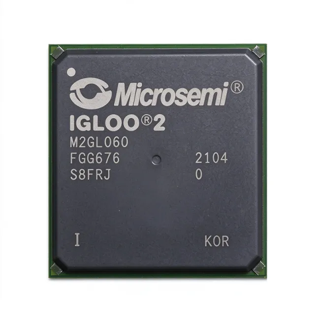
M2GL060-FGG484
M2GL060-FGG484 - 56.5K Logic Cells | Microchip | Industrial
The Microchip Technology M2GL060-FGG484 is an IGLOO 2 flash-based field-programmable gate array with 56,520 logic elements, 267 user I/Os, and a 1.2 V operating supply in a 484-ball FBGA package. It is designed for compact, low-power programmable logic in industrial, communications, medical, defense, and aviation systems. The device combines a reusable nonvolatile configuration architecture with 267 I/Os, allowing designers to implement protocol bridging, I/O expansion, interface conversion, video and image processing, system management, and secure connectivity without relying on an external configuration device.
An FPGA is a programmable semiconductor whose logic fabric, interconnect network, and peripherals can be configured after fabrication. This makes the FPGA hierarchy broader than a fixed-function logic IC. The M2GL060-FGG484 belongs to the IGLOO 2 low-density FPGA family, where flash configuration memory provides a practical single-chip implementation for moderate logic density. Its 267 I/Os provide substantial board-level connectivity, while the 484-ball FBGA supports dense routing in space-constrained equipment.
The headline implementation advantages are the 56,520 logic elements, 267 user I/Os, and 1.2 V supply requirement. These figures allow complex control paths, parallel data processing, and multiple external interfaces to coexist in one device. The M2GL060-FGG484 is particularly useful when a design needs more flexibility than an application-specific controller but does not justify the power, cost, and complexity of a much larger FPGA. Its surface-mount 484-ball package also supports automated assembly and high-density PCB layouts.
Microchip positions IGLOO 2 devices for general-purpose functions including Gigabit Ethernet or dual PCI Express control planes, bridging, I/O expansion and conversion, image processing, system management, and secure connectivity. Because configuration is stored in flash, the device can support deterministic startup behavior without a separate configuration PROM. Engineers should still account for configuration pins, dedicated programming resources, bank voltage constraints, and the pin requirements of their selected interfaces when planning the PCB.
Typical uses include industrial communication gateways, medical monitoring equipment, defense and aviation subsystems, video-capture interfaces, secure network access equipment, and embedded control systems. The device can consolidate multiple fixed-function logic blocks into one programmable implementation, simplifying board partitioning and allowing firmware or configuration updates during product maintenance. Its low-density positioning makes it well matched to control-plane logic, sensor aggregation, and protocol translation rather than large parallel-compute workloads.
A key design consideration is that the complete BGA pin assignment, bank architecture, and electrical constraints must be taken directly from the manufacturer pin-description guide. Confirm every power, ground, configuration, clock, and user-I/O connection before layout release. High-speed interfaces also require disciplined return-path planning, while the 1.2 V core supply requires a regulator and decoupling network designed for the device's transient requirements.
This page consolidates the manufacturer's device identity, family application guidance, lifecycle status, package information, and verified cross-reference information. It also provides parameter-level comparisons, drop-in migration notes, and practical design guidance for engineers evaluating the M2GL060-FGG484 against same-family speed and temperature-grade options.
Devis
Contact