Produits (32821)

AD574AJDZ - 12-Bit SAR ADC, 28-CDIP | Analog Devices
AD574AJDZ

AD574AJDZ - 12-Bit SAR ADC, 28-CDIP | Analog Devices

The Analog Devices AD574AJDZ is a complete 12-bit successive-approximation-register (SAR) analog-to-digital converter integrating a buried Zener precision reference, an internal clock, and 3-state output buffers for direct 8/16-bit microprocessor bus interface, all in a hermetic 28-pin ceramic DIP (28-CDIP) package. The J-grade device operates over -55C to +125C, and the AJDZ suffix indicates the ceramic side-brazed DIP package, J-temperature grade, and the factory die revision marking scheme. An SAR analog-to-digital converter is a type of data converter that performs a binary search across an internal capacitive DAC to digitize an analog input in N clock cycles, where N equals the converter resolution. Compared with flash, sigma-delta, and dual-slope architectures, the SAR topology combines high throughput (tens to hundreds of ksps), low latency, no pipeline delay, and excellent DC linearity - making it the dominant architecture for 12-16 bit precision measurement, industrial data acquisition, and instrumentation applications. The AD574A family is widely regarded as the industry-standard 12-bit ADC and has been in continuous production since the early 1980s. Key features of the AD574AJDZ include 12-bit resolution with 35 us maximum conversion time, factory-calibrated linearity (no missing codes), four software-configurable input ranges (0 to +10 V, 0 to +20 V, -5 to +5 V, -10 to +10 V), and 8/16-bit microprocessor bus compatibility with standard read/write control logic. The on-chip reference and clock eliminate two of the largest external component costs typical of older 12-bit ADC designs. Architecturally, the AD574A combines a precision laser-trimmed thin-film DAC, a high-speed comparator, a successive-approximation register, and a 10 V buried Zener reference - all on a single bipolar/CMOS die. This integration produces full-rated performance without user calibration, a major advantage over the modular ADC boards of the era. The hermetic 28-CDIP package supports the J-grade (-55C to +125C) temperature range required for military and aerospace programs. Typical applications include precision industrial data acquisition systems, military/aerospace avionics signal conditioning, automated test equipment (ATE), process-control front ends, and high-reliability instrumentation requiring the extended-temperature ceramic package. The wide input range and 12-bit linearity suit multi-channel multiplexed front ends with PGA conditioning. When designing with the AD574AJDZ, allocate 200 ns bus-access timing margins and place a 100 nF bypass capacitor within 5 mm of each supply pin to suppress the high-current switching transients inherent to the SAR architecture. The ceramic DIP is intended for through-hole sockets on MIL-STD-810 and MIL-PRF-38534 compliant boards; for surface-mount designs, the AD574AUD (28-SOIC) is a recommended drop-in electrical equivalent.

Devis Contact
AD574AJE - 12-Bit ADC, 28-Pin LCC | Analog Devices
AD574AJE

AD574AJE - 12-Bit ADC, 28-Pin LCC | Analog Devices

The Analog Devices AD574AJE is a complete 12-bit successive-approximation analog-to-digital converter (SAR ADC) with integrated buried-Zener voltage reference, internal clock, and three-state output buffers, housed in a 28-terminal ceramic leadless chip carrier (LCC / QCCN / JLCC) package. The JEDEC JESD30 code QCCN denotes a square, no-lead chip-carrier package, and the JE suffix designates the commercial 0C to +70C temperature grade. An ADC (analog-to-digital converter) is a data converter that translates continuous analog signals into discrete digital codes. The AD574A family belongs to the successive-approximation register (SAR) architecture, which uses a comparator, an internal DAC, and a successive-approximation register to converge on the input voltage in N bit-clock cycles. SAR ADCs sit in the broader converter hierarchy: data converter -> ADC -> Nyquist ADC -> successive-approximation ADC -> integrated ADC with reference. They are valued for high accuracy, deterministic latency, and ease of microprocessor interfacing, making them a staple of industrial-instrumentation and process-control designs since the mid-1980s. Key features include guaranteed no-missing-codes operation over temperature, full 12-bit linearity maintained across the commercial range, and a maximum conversion time of 35 us using the on-chip clock. The integrated buried-Zener reference delivers long-term stability better than bandgap-only designs, eliminating the need for an external reference component. Three-state output buffers allow direct connection to 8- or 16-bit microprocessor data buses without additional glue logic, and standard +/-10 V or 0 V to +10 V / 0 V to +20 V analog input ranges are pin-selectable. The device implements a classic two-pass successive-approximation loop and an on-chip bipolar-offset DAC, enabling true bipolar input ranges from a single +5 V and +/-15 V analog supply. Its monolithic construction removes the calibration overhead typical of hybrid or modular ADC solutions, while the integrated clock and reference simplify PCB design and lower BOM count. Typical applications include process-control front ends, weigh-scale and load-cell digitizers, portable instrumentation, laboratory data loggers, and any 8- or 16-bit microprocessor-based measurement system requiring a complete, board-level 12-bit acquisition channel. Designers should choose the AD574AJE when a fully integrated, calibrated ADC with on-chip reference is preferred over a discrete ADC + external reference solution, and when the LCC footprint is acceptable for the assembly process.

Devis Contact
AD574ASE/883B - 12-Bit SAR ADC, Military Grade | Analog Devices
AD574ASE/883B

AD574ASE/883B - 12-Bit SAR ADC, Military Grade | Analog Devices

The AD574ASE/883B is a complete 12-bit successive-approximation analog-to-digital converter (ADC) from Analog Devices, designed for high-reliability military and aerospace applications. It integrates a precision voltage reference, clock, and 3-state output buffers for direct interface to 8- or 16-bit microprocessor buses. The device operates over the full military temperature range of -55°C to +125°C and is available in a 28-lead ceramic LCC (11.43x11.43 mm) package, with screening to MIL-STD-883 Class B. An ADC (analog-to-digital converter) is an electronic component that converts continuous analog signals into discrete digital values. The AD574A family is a classic example of a successive-approximation register (SAR) ADC, which uses a binary search algorithm to determine the digital output. SAR ADCs are known for their good balance of speed, resolution, and power consumption, making them suitable for a wide range of data acquisition systems. The AD574A is a complete converter, meaning it includes all necessary functions on-chip, such as the reference and clock, simplifying system design. Key features of the AD574ASE/883B include 12-bit resolution, a maximum conversion time of 35 microseconds, and guaranteed no missing codes over temperature. It supports both 8-bit and 16-bit microprocessor bus interfaces, allowing flexible integration with various digital systems. The device also offers a bipolar input range of -10V to +10V, making it suitable for industrial and instrumentation applications. The military-grade screening ensures reliable operation in harsh environments. Technically, the AD574A uses a laser-trimmed thin-film resistor network and an internal reference to achieve high accuracy. The device is designed to operate without external components for the reference and clock, reducing system complexity. The 3-state output buffers allow direct connection to a data bus, and the device can be configured for either 8-bit or 16-bit data transfer. The military version (883B) undergoes additional testing and screening to meet stringent reliability standards. Typical applications include military avionics, radar systems, industrial process control, and test and measurement equipment. The wide input range and high accuracy make it ideal for precision data acquisition in harsh environments. The device's robustness and long-term availability (often through authorized distributors like Rochester Electronics) make it a preferred choice for legacy system maintenance. When designing with the AD574ASE/883B, ensure proper decoupling on the power supply pins and a clean analog ground plane to minimize noise. The reference and clock are internal, but external bypass capacitors are recommended for optimal performance. Also, consider the conversion time of 35 µs when planning system throughput.

Devis Contact
AD574ATE/883B - 12-Bit SAR ADC, Military Grade | Analog Devices
AD574ATE/883B

AD574ATE/883B - 12-Bit SAR ADC, Military Grade | Analog Devices

The AD574ATE/883B is a complete 12-bit successive-approximation analog-to-digital converter (ADC) manufactured by Analog Devices Inc. It integrates all analog and digital functions on a single chip using Analog Devices' Bipolar/I2L process, including a high-precision voltage reference and clock, ensuring full-rated performance without external circuitry. The device features a 3-state output buffer for direct interface to an 8- or 16-bit microprocessor bus, making it ideal for industrial and military data acquisition systems. Housed in a 28-lead ceramic leadless chip carrier (LCC) with dimensions 11.43x11.43 mm, it operates over the military temperature range and is processed to MIL-STD-883C Class B standards. An analog-to-digital converter (ADC) is an electronic component that converts continuous analog signals into discrete digital numbers. The AD574A is a successive-approximation ADC, which uses a binary search algorithm to determine the digital output, offering a good balance of speed and resolution. As a 12-bit ADC, it provides 4096 discrete levels, enabling high-resolution measurement of analog signals. This device belongs to the family of data acquisition components, which are essential in bridging the analog and digital domains in systems such as industrial process control, military avionics, and scientific instrumentation. Key features of the AD574ATE/883B include 12-bit resolution, a single input channel, and a successive-approximation register (SAR) architecture. It operates from a bipolar power supply, and its parallel word access allows for fast data transfer to microprocessors. The device is available in a 28-LCC package, which is suitable for surface-mount assembly and provides good thermal and electrical performance. The military-grade processing ensures reliability in harsh environments, with a temperature grade of MILITARY, indicating operation from -55°C to +125°C. Technically, the AD574A integrates a precision voltage reference and clock on-chip, eliminating the need for external components. The Bipolar/I2L process enables high-speed operation and low power consumption. The device includes a 3-state output buffer, allowing direct connection to a microprocessor bus without additional interface logic. The conversion time is typically 25 microseconds, providing a throughput of 40 kSPS. The device also features a status output to indicate when conversion is complete, simplifying system integration. Typical applications include military avionics, industrial process control, medical instrumentation, and scientific data acquisition systems. The AD574ATE/883B is particularly suited for applications requiring high accuracy and reliability in extreme environments, such as aerospace and defense systems. Its parallel interface simplifies connection to microcontrollers and DSPs, making it a versatile choice for embedded systems. When designing with this device, ensure proper decoupling of the power supply pins and a clean analog ground to achieve specified accuracy. The reference voltage is internally generated, but external filtering may be required for optimal performance. The device is not RoHS compliant due to its military-grade hermetic package, which is a consideration for applications with environmental compliance requirements.

Devis Contact
AD582SH/883B - Military Sample-and-Hold Amplifier | Analog Devices
AD582SH/883B

AD582SH/883B - Military Sample-and-Hold Amplifier | Analog Devices

The AD582SH/883B is a military-grade sample-and-hold amplifier manufactured by Analog Devices, designed for precision data acquisition systems requiring high accuracy and reliability. It integrates a high-performance operational amplifier, a low-leakage analog switch, and a JFET integrating amplifier on a single monolithic chip, with an external holding capacitor completing the sample-and-hold function. The device operates from a nominal ±15V supply, features a maximum acquisition time of 6 µs, and is specified over the full military temperature range of -55°C to +125°C. Housed in a 10-pin TO-100 metal can package, it provides separate analog and digital grounds to improve immunity to ground and switching transients, making it ideal for harsh environments. A sample-and-hold amplifier (SHA) is an analog circuit that captures the voltage of an input signal at a specific instant and holds it constant for a defined period, enabling accurate conversion by an analog-to-digital converter (ADC). It is a critical building block in data acquisition systems, where it bridges the gap between fast-changing analog signals and the finite conversion time of ADCs. The AD582SH/883B belongs to the family of sample-and-hold circuits, which are essential in applications such as automatic test equipment, medical instrumentation, and military avionics. Key features of the AD582SH/883B include its MIL-STD-883 compliance, ensuring reliability under extreme conditions, and its separate analog and digital grounds, which minimize noise coupling. The device offers a maximum acquisition time of 6 µs, allowing it to track fast signals, and a maximum supply current of 4.5 mA, making it power-efficient for its class. The TO-100 metal can package provides robust hermetic sealing, protecting the internal circuitry from moisture and contaminants. Technically, the AD582SH/883B uses bipolar technology, which offers high-speed performance and low offset voltage. The internal JFET integrating amplifier provides high input impedance, reducing loading on the signal source. The low-leakage analog switch ensures minimal droop rate, maintaining the held voltage accurately over time. The device's architecture is optimized for precision, with careful attention to charge injection and aperture error, which are critical for high-resolution sampling. Typical applications include military radar systems, aerospace telemetry, and industrial process control, where the device's ruggedness and precision are paramount. In these systems, the AD582SH/883B is used to sample analog sensor signals and hold them for digitization, ensuring accurate measurement even in noisy environments. When designing with the AD582SH/883B, it is essential to select an appropriate external holding capacitor to balance acquisition time and droop rate. A larger capacitor reduces droop but increases acquisition time, while a smaller capacitor improves speed but may compromise hold stability. Additionally, proper grounding and decoupling are critical to maintain the device's noise immunity.

Devis Contact
AD5933YRSZ - 1MSPS 12-bit Impedance Converter, 16-SSOP
AD5933YRSZ

AD5933YRSZ - 1MSPS 12-bit Impedance Converter, 16-SSOP

The Analog Devices AD5933YRSZ is a high-precision 1 MSPS, 12-bit impedance converter and network analyzer housed in a 16-pin SSOP (RS) package, combining an on-board programmable frequency generator, a 12-bit analog-to-digital converter (ADC), and a discrete Fourier transform (DFT) engine on a single chip. The excitation frequency can be set up to 16.776 MHz, allowing an external complex impedance to be stimulated with a known sine wave; the response is sampled and processed by an on-chip DFT to extract real and imaginary impedance components. Key headline parameters are: 1 MSPS ADC, 12-bit resolution, and a 16.776 MHz maximum MCLK. The device operates from 2.7 V to 5.5 V supply and supports I2C and SPI serial interfaces for register configuration. An impedance converter network analyzer is a mixed-signal subsystem that synthesizes a sine stimulus, applies it to an external unknown impedance (typically via a precision front-end op-amp and transimpedance gain resistor), and uses an ADC plus on-chip DFT to extract the impedance's real and imaginary components at each frequency. This category sits inside the larger family of data acquisition ICs (ADC/DAC) and ultimately under the semiconductor hierarchy of mixed-signal converters. Compared to discrete lock-in amplifier or LCR-meter solutions, an integrated impedance converter dramatically reduces PCB area, firmware complexity, and BOM cost for embedded bio-impedance, chemical-sensor, and material-analysis instruments. The AD5933 is the industry-standard example of this category. Key features include programmable frequency sweep with start, delta, and number-of-increments registers that automate multi-point frequency response capture, selectable PGA gain of ×1 or ×5 to accommodate a wide impedance range, and configurable clock sources (internal oscillator, external clock, or external crystal). Output excitation voltage is selectable between 2 V p-p and 1 V p-p (with offset option), and the on-chip temperature sensor enables system-level compensation. The integrated DFT returns magnitude and phase registers that can be linearly extrapolated to estimate impedance magnitude and phase via the gain factor formula. Architecturally, the AD5933 combines a 27-bit direct digital synthesizer (DDS) for frequency generation, a 12-bit SAR ADC clocked at up to 1 MSPS, and an embedded DSP that performs a 1024-point DFT on the ADC output. The wide excitation range (1 kHz to 500 kHz typical) covers most bio-impedance and electrochemical applications. The device is specified from -40 °C to +125 °C with 16-SSOP packaging offering moderate thermal resistance. Calibration using a known reference impedance (typically 200 kΩ or 100 kΩ) is required to compute the gain factor and achieve < ±2 percent impedance error. Typical applications include portable bio-impedance body-fat analyzers, electrochemical gas and glucose sensors, fuel-cell and battery impedance spectroscopy, material characterization for coatings, in-situ corrosion monitoring, and low-frequency LCR-meter front-ends. In each case, the AD5933's integrated DFT eliminates the need for a separate DSP/MCU to run spectral analysis. Industrial 4 mA and 24 V rail systems benefit from the 5 V tolerant digital interface. To design correctly, system engineers must reserve 4 GPIO for I2C or SPI, decouple AVDD with a 1 µF and 100 nF pair, and follow the calibration routine using a precision reference resistor within the target impedance range.

Devis Contact
AD5934YRSZ - 250 kSPS 12-Bit Impedance Converter | Analog Devices
AD5934YRSZ

AD5934YRSZ - 250 kSPS 12-Bit Impedance Converter | Analog Devices

The Analog Devices AD5934YRSZ is a 250 kSPS, 12-bit impedance converter and network analyzer that combines an on-board frequency generator with a 12-bit, 250 kSPS analog-to-digital converter (ADC). Housed in a 16-pin SSOP package (YRS suffix), the device is specified for operation from a 3.3 V supply with an external MCLK up to 16.776 MHz, and it produces an excitation output up to 50 kHz for sweeping an unknown complex impedance. The integrated discrete Fourier transform (DFT) engine returns calibrated real and imaginary 16-bit words per frequency point, allowing a host microcontroller to compute magnitude and phase. An impedance analyzer is an instrument class that measures the complex impedance (resistance plus reactance) of a component, sensor, or biological sample across a range of AC frequencies. Within the broader instrumentation hierarchy, the AD5934 sits between a discrete lock-in amplifier and a full benchtop LCR meter: it removes the need for a separate function generator, digitizer, and FFT processor while still delivering calibrated magnitude/phase data over a user-selected frequency sweep. This integration is what makes it attractive for embedded electrochemical, bioimpedance, and material-sensing products. Key specifications include 12-bit ADC resolution at 250 kSPS, an excitation amplitude programmable in four steps from 0.2 V p-p to 2.0 V p-p, a programmable gain amplifier (PGA) with x1 or x5 settings, an I2C-compatible serial interface, and an operating temperature range of -40C to +125C. The on-chip temperature sensor (TA pin) and dedicated system clock input allow designers to add temperature compensation and reject mains-related clock jitter in the same BOM. Architecturally, the AD5934 separates the excitation DAC, the transimpedance front end (with external RFB), the sampling ADC, and the DSP DFT block, all clocked from a single MCLK reference. The result is a system whose accuracy is determined by the external calibration resistor (typically 200 kohm between RFB and VIN), the stability of the MCLK source, and the impedance range selected via the gain resistor - not by any factory trim step, which simplifies board bring-up. Typical applications include bioimpedance and skin-conductance analysis, electrochemical sensor interfaces, in-line material moisture meters, portable LCR-style probes, and multi-frequency material identification. Engineers choose the AD5934 when they need calibrated magnitude/phase data without the cost, size, or power budget of a bench instrument. When designing with the part, place the calibration resistor close to the RFB and VIN traces and drive MCLK from a low-jitter source; this is the single biggest determinant of sweep-to-sweep repeatability. This page synthesizes distributor pricing, qualified drop-in alternatives, and practical layout notes not collected in the standalone datasheet PDF.

Devis Contact
AD5934YRSZ-REEL7 - 250kSPS 12-Bit Impedance Converter | ADI
AD5934YRSZ-REEL7

AD5934YRSZ-REEL7 - 250kSPS 12-Bit Impedance Converter | ADI

The Analog Devices AD5934YRSZ-REEL7 is a high-precision 12-bit, 250 kSPS impedance converter and network analyzer system-on-chip that combines an on-board programmable frequency generator with a 12-bit analog-to-digital converter (ADC) and an on-chip DSP engine for discrete Fourier transform (DFT) processing, all integrated into a 16-pin SSOP package. The device excites an external complex impedance with a known frequency up to 50 kHz, samples the response signal, and returns calibrated real and imaginary impedance words via I²C/SPI serial interface, eliminating the need for external signal conditioning and reducing the BOM for portable bio-impedance and material analysis designs. An impedance converter network analyzer is a specialized data acquisition system that performs synchronous sine excitation, current-to-voltage conversion, and discrete Fourier transform (DFT) processing to extract magnitude and phase information from a connected unknown impedance. As a member of the impedance analyzer / LCR meter IC family, it sits at the intersection of the broader categories of direct digital synthesis (DDS), signal chain analog-to-digital converter (ADC), and embedded DSP, which together form a complete vector impedance measurement sub-system. The AD5934 in particular integrates DDS, transimpedance amplifier, ADC, and DFT engine into one IC. Key specifications include 12-bit ADC resolution, 250 kSPS sampling rate, programmable excitation output frequency up to 50 kHz, 16.776 MHz internal clock or external MCLK input, on-chip temperature sensor with ±2 °C precision, and serial interface compatibility with I²C or SPI protocols. The device supports a system clock from 0.1 MHz to 16.776 MHz and is supplied from a single 2.7 V to 5.5 V rail, equivalent to most 3 V or 5 V logic rails. The internal DDS allows 0.1 Hz frequency resolution when clocked from the on-chip oscillator. The excitation amplitude is programmable in four discrete steps between 0.2 Vpp and 1.98 Vpp to accommodate different impedance ranges. The AD5934 architecture combines a 28-bit direct digital synthesizer (DDS) core, a low-noise transimpedance front-end, a 12-bit successive-approximation ADC, and an embedded DFT processor that returns calibrated real (R) and imaginary (I) 16-bit words per frequency point. Gain factor calibration using a reference impedance removes system gain error across the 100 Ω to 10 MΩ measurement range, equivalent to a four-decade dynamic span, while the embedded temperature sensor compensates for system drift across the -40 °C to +125 °C automotive-grade operating range. The serial interface supports both standard I²C (100 kHz) and SPI (up to 5 MHz) for flexible host connectivity. Typical applications include portable bio-electrical impedance analysis (BIA) for body composition scales and fitness monitors, in-vitro electrochemical biosensors for glucose and pathogen detection, industrial material moisture and soil moisture analysis, fuel cell and battery impedance spectroscopy for state-of-charge estimation, and on-board diagnostic (OBD) systems for automotive sensor health monitoring. Compared to discrete lock-in amplifier solutions, the AD5934 reduces board area, BOM count, and firmware complexity by integrating the entire excitation-acquisition-DFT pipeline into one SSOP-16 package, while preserving calibration-grade accuracy through its gain factor compensation routine. When designing with the AD5934, place a precision 200 Ω or 100 kΩ reference resistor between the excitation output (IOUT) and the ADC input (VIN) for system calibration, and use the temperature sensor reading to correct for thermal drift of the reference resistor. The RFB pin selects the transimpedance gain; pair it with a low-temperature-coefficient external feedback resistor to extend the impedance measurement range beyond 1 MΩ. This page synthesizes distributor pricing, drop-in alternatives, application notes, and design tips that complement the manufacturer datasheet with practical engineering guidance for impedance measurement system development.

Devis Contact
AD620ANZ - 1-Channel Low-Power Instrumentation Amplifier | Analog Devices
AD620ANZ

AD620ANZ - 1-Channel Low-Power Instrumentation Amplifier | Analog Devices

The Analog Devices AD620ANZ is a one-channel, low-cost instrumentation amplifier in an 8-lead PDIP package, with programmable gains from 1 to 10,000 using one external resistor and a maximum supply current of 1.3 mA. Its 1 MHz bandwidth and high input impedance make it suitable for precision measurement, sensor conditioning, biomedical instrumentation, and industrial signal acquisition. The device is specified as a low-cost, low-power, high-accuracy instrumentation amplifier. The AD620 family uses an internal resistor network to set gain, simplifying analog front-end design while preserving accurate differential amplification. An instrumentation amplifier is a specialized analog amplifier optimized for measuring a small differential signal embedded in a larger common-mode voltage. Its internal subtractor, input buffers, and feedback network provide high input impedance, common-mode rejection, and gain accuracy while reducing the number of precision external components. The AD620 belongs to the broader signal-conditioning and amplifier hierarchy and is commonly placed between sensors and analog-to-digital converters, where accurate amplification is required before sampling. The verified manufacturer and distributor information identifies the AD620 as supporting gains from 1 to 10,000, 1 MHz bandwidth, and low-power operation. The AD620ANZ is supplied in an 8-lead PDIP package, while the AD620 family is also offered in 8-lead SOIC packaging. The single-external-resistor gain-setting arrangement allows the same device family to serve both low-gain buffering and high-gain sensor applications. The device is intended for systems where low cost and low power are important without sacrificing the basic precision expected from an instrumentation amplifier. A typical circuit accepts differential sensor outputs at the input pins, uses an external gain resistor between the gain-setting pins, and drives an analog-to-digital converter or measurement subsystem. Proper layout is important because high-impedance input nodes should be kept short, clean, and away from high-current switching paths. The supply rails and bypass capacitors should be placed close to the device, while the gain resistor should be positioned according to the manufacturer’s recommended layout. The verified data does not provide complete electrical limits, pin names, temperature ratings, or supply-voltage values, so those parameters are marked as data needed rather than inferred. Typical applications include bridge and pressure sensor interfaces, biomedical signal acquisition, current measurement, portable instrumentation, and precision data-acquisition systems. The AD620ANZ is particularly suitable where the measured differential signal is small and the surrounding system includes meaningful common-mode voltage. Compared with a discrete three-op-amp implementation, the integrated instrumentation amplifier reduces board area and component count while providing a defined gain-setting method. The manufacturer product page and distributor listings are the primary sources for this component overview; use the manufacturer datasheet for complete electrical characteristics, pinout, and application limits. This product page combines verified manufacturer and distributor information with practical application guidance and source-linked buying context. It does not infer unprovided electrical values, package dimensions, lifecycle claims, or pricing amounts. For an exact replacement, verify the manufacturer pinout, supply range, gain equation, common-mode range, output swing, temperature grade, and availability before substituting any part.

Devis Contact
AD620ARZ - Low Cost Low Power Instrumentation Amplifier | Analog Devices
AD620ARZ

AD620ARZ - Low Cost Low Power Instrumentation Amplifier | Analog Devices

The AD620ARZ is a low cost, high accuracy instrumentation amplifier from Analog Devices, designed for applications requiring precise amplification of small differential signals in the presence of common-mode noise. It is available in an 8-lead SOIC package and operates from a single or dual supply ranging from ±2.3V to ±18V. The gain is set by a single external resistor, allowing gains from 1 to 10,000, making it highly versatile for various sensor interface applications. An instrumentation amplifier is a type of differential amplifier that amplifies the difference between two input signals while rejecting common-mode voltages. It is characterized by high input impedance, high common-mode rejection ratio (CMRR), and low offset voltage, making it ideal for precision measurement systems. The AD620 belongs to the family of instrumentation amplifiers, which are essential building blocks in analog signal conditioning chains, often used after sensors such as strain gauges, thermocouples, and pressure sensors. Key features of the AD620ARZ include a maximum supply current of 1.3 mA, making it suitable for battery-powered and portable applications. It offers a CMRR of 100 dB at gain of 10, and a low input offset voltage of 50 µV. The device also features low input bias current of 1.0 nA, and a bandwidth of 120 kHz at gain of 10. The AD620ARZ is specified over the industrial temperature range of -40°C to +85°C. Technically, the AD620 uses a classic three-op-amp topology with an internal precision resistor network, achieving excellent gain accuracy and stability. The gain is set by an external resistor RG, with the formula G = 1 + 49.4 kΩ/RG. This architecture provides high input impedance (10 GΩ) and low noise, with a voltage noise density of 9 nV/√Hz at 1 kHz. The device is laser-trimmed for low offset voltage and drift, ensuring high precision over temperature. Typical applications include medical instrumentation (ECG, EEG), industrial process control, transducer interfaces, and data acquisition systems. The AD620ARZ is particularly suited for applications where low power consumption and high accuracy are critical, such as portable medical devices and remote sensor nodes. When designing with the AD620ARZ, it is important to provide proper decoupling on the power supply pins and to keep the input traces short and shielded to minimize noise pickup. The gain resistor should be placed close to the device to reduce parasitic capacitance and maintain accuracy.

Devis Contact
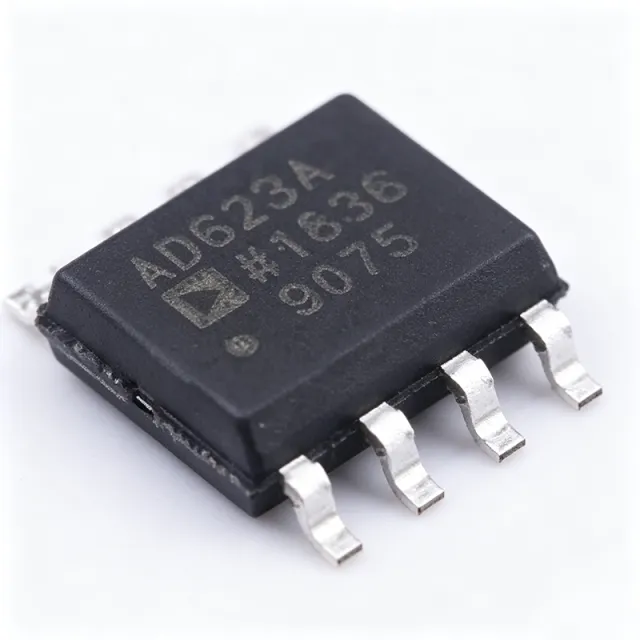
AD623ANZ - 8-Pin Instrumentation Amplifier | Analog Devices
AD623ANZ

AD623ANZ - 8-Pin Instrumentation Amplifier | Analog Devices

The Analog Devices AD623ANZ is a single-circuit instrumentation amplifier with rail-to-rail output swing, single- or dual-supply operation, and an 8-PDIP package. The verified manufacturer data specifies a supply range of 2.7 V to 12 V, with 3 V to 12 V also identified for the integrated single-supply configuration. Its gain can be programmed with one external resistor, and the device accepts industry-standard 8-lead instrumentation-amplifier pin arrangements. These characteristics make it suitable for sensor-frontend, measurement, and signal-conditioning systems where common-mode rejection and differential input handling are required. An instrumentation amplifier is a specialized analog amplifier optimized for amplifying a small differential signal riding on a larger common-mode voltage. In the signal-chain hierarchy, an instrumentation amplifier belongs to the amplifier family and supports precision measurement, bridge excitation, biomedical instrumentation, and industrial sensing. The AD623 combines that differential-input function with rail-to-rail output capability, allowing the output to approach the supply limits under suitable load conditions. The AD623 is designed for low-power analog systems and provides user flexibility through a single gain-setting resistor. The AD623ANZ package designation identifies the Analog Devices orderable variant listed by DigiKey as an 8-PDIP device. The manufacturer page describes rail-to-rail output swing and supply operation from 2.7 V to 12 V, while the AD623 datasheet identifies the device as a single- or dual-supply, rail-to-rail, low-cost instrumentation amplifier. Instrumentation-amplifier performance depends on matching internal resistor networks, input bias behavior, gain accuracy, bandwidth, and the voltage headroom available around the input and output. Because the verified sources provide only high-level product and supply information, exact gain error, noise density, common-mode rejection, input bias current, bandwidth, and temperature limits must be confirmed against the manufacturer datasheet before design release. The AD623 datasheet is the authoritative source for those electrical characteristics. Typical uses include bridge-based pressure and load sensing, low-level transducer amplification, battery-powered measurement equipment, and industrial signal conditioning. In a bridge circuit, the AD623 can amplify the small differential bridge output while rejecting the larger common-mode voltage. Designers should check input common-mode range, output swing, gain equation, supply voltage, and external resistor tolerance against the exact operating condition. For PCB implementation, preserve the manufacturer-recommended pin assignments and provide short, low-noise routing between the sensor source, gain resistor, supply bypass network, and output receiver. A clean analog ground return and adequately decoupled supply rails help preserve measurement integrity. This page combines verified manufacturer and distributor information with engineering selection guidance, while clearly separating confirmed values from parameters still requiring datasheet confirmation.

Devis Contact
AD623ARZ-R7 - Rail-to-Rail In-Amp, 3-12V | Analog Devices
AD623ARZ-R7

AD623ARZ-R7 - Rail-to-Rail In-Amp, 3-12V | Analog Devices

The Analog Devices AD623ARZ-R7 is a single-supply, rail-to-rail output instrumentation amplifier with a 2.7 V to 12 V supply range, 800 kHz bandwidth, and 90 dB minimum CMRR at G = 1, housed in an industry-standard 8-lead SOIC package (3.90 mm width). An instrumentation amplifier (in-amp) is a type of differential amplifier that amplifies the difference between two input signals while rejecting common-mode voltages. Characterized by high input impedance, high common-mode rejection ratio (CMRR), and low offset voltage, in-amps form a specialized subclass within the operational amplifier family and are essential building blocks in analog signal conditioning chains for precision sensing. Key features of the AD623ARZ-R7 include gain programming with a single external resistor via the formula G = 1 + 100 kOhm/RG (unity gain with no external resistor), rail-to-rail output swing, and input common-mode range extending 150 mV below ground on a single supply. It operates from single supplies of 3 V to 12 V or dual supplies of +/-2.5 V to +/-6 V, suiting both portable and industrial systems. Technically, the AD623 uses a classic three-op-amp topology with a laser-trimmed internal precision resistor network. The input stage provides high impedance and excellent CMRR, while the output stage delivers rail-to-rail swing. The REF terminal allows low-impedance level shifting of the output, critical for centering signals in single-supply data acquisition systems. A and B grades differ in offset voltage and drift specifications. Typical applications include load cell and pressure sensor signal conditioning, medical ECG front ends, thermocouple amplification, and industrial process control, where the high CMRR rejects common-mode noise in electrically noisy environments. When designing, place the gain resistor close to the device, bypass each supply pin with 0.1 uF, and drive the REF pin from a low-impedance source to preserve CMRR. This page synthesizes distributor pricing, drop-in alternatives, and practical design notes not found in the manufacturer datasheet.

Devis Contact
AD629ARZ-R7 - ±270V Common-Mode Diff Amp SOIC-8 | ADI
AD629ARZ-R7

AD629ARZ-R7 - ±270V Common-Mode Diff Amp SOIC-8 | ADI

The Analog Devices AD629ARZ-R7 is a precision difference amplifier rated for ±270 V common-mode input voltage in an 8-pin SOIC (R-7 tape & reel) package. It delivers 86 dB minimum DC CMRR, 1 V/V fixed unity gain, and 2.1 V/µs slew rate from a ±2.5 V to ±18 V dual supply. The device is an improved pin-for-pin replacement for the legacy INA117P and INA117KU. A difference amplifier is a specialized op-amp topology that subtracts two input signals and rejects the common-mode voltage present on both inputs. In the broader IC taxonomy it belongs to the instrumentation amplifier family (in-amp -> difference amplifier -> operational amplifier -> analog IC -> semiconductor). The AD629 specifically targets high common-mode industrial environments where signal levels up to ±270 V must be rejected to extract a small differential signal sitting on top of a large DC bus. Key features include ±270 V continuous common-mode range, 86 dB minimum CMRR (DC to 1 kHz), 500 kHz small-signal bandwidth, 2.1 V/µs slew rate, and integrated precision resistor networks that set unity gain without external components. The internal laser-trimmed thin-film resistors achieve 0.03% typical gain accuracy and excellent common-mode rejection over temperature. The AD629 uses a three-op-amp topology with input overvoltage protection through internal resistors and ESD clamps. Its supply current of approximately 1 mA (per amplifier, single gain stage active) keeps self-heating low, while the SOIC-8 (θJA = 155 °C/W) package is rated for -40 °C to +85 °C operation. Typical applications include motor control phase current sensing, 48 V/24 V battery monitoring, shunt-based high-side current measurement, industrial PLC analog front ends, and power inverter feedback. Designers choose it when they need to digitize a small differential signal riding on a high-voltage DC bus. Designers should ground both REF pins (1 and 5) to a low-impedance ground plane and leave pin 8 floating (NC). Using separate ground returns for input signal ground and REF ground degrades CMRR by tens of dB. This page synthesizes distributor pricing, drop-in alternatives, and PCB layout guidance not available from the manufacturer datasheet alone.

Devis Contact
AD632SH/883B - Precision 4-Quadrant Multiplier | Analog Devices
AD632SH/883B

AD632SH/883B - Precision 4-Quadrant Multiplier | Analog Devices

The AD632SH/883B is an internally trimmed precision monolithic four-quadrant analog multiplier/divider from Analog Devices, packaged in a hermetic TO-100-10 metal can. It is pin-for-pin compatible with the industry-standard AD532 but offers improved specifications, including a fully differential high-impedance Z-input. The device can provide gains up to ×10, often eliminating the need for separate instrumentation amplifiers to precondition inputs. It operates over the military temperature range of -55°C to +125°C and is available in a through-hole TO-100-10 package. An analog multiplier is a circuit that produces an output voltage proportional to the product of two input voltages. The AD632 is a four-quadrant multiplier, meaning it can handle both positive and negative input signals, enabling applications such as modulation, demodulation, automatic gain control, and power measurement. As a precision analog computational building block, it sits within the broader category of analog signal processing ICs, which are essential in instrumentation, control systems, and communication equipment. Key features include excellent long-term stability, low noise, and high reliability. The device is internally trimmed for accuracy, reducing the need for external calibration. The fully differential Z-input allows flexible signal conditioning, and the ability to achieve gains up to ×10 simplifies system design. The TO-100-10 metal can package provides hermetic sealing, making it suitable for harsh environments. Technically, the AD632 uses a monolithic bipolar process with laser-trimmed thin-film resistors to achieve high accuracy. The transfer function is W = (X1 - X2)(Y1 - Y2)/10V + Z, where Z is the differential Z-input. This architecture supports multiplication, division, squaring, and square-rooting functions. The device is designed for precision analog computation, with a typical nonlinearity of ±0.5% and a small-signal bandwidth of 1 MHz. Typical applications include analog computation in test and measurement equipment, precision power measurement, process control, and signal conditioning in military and aerospace systems. The AD632SH/883B is particularly suited for applications requiring high accuracy and stability over a wide temperature range. When designing with this device, ensure proper power supply decoupling with 0.1 µF ceramic capacitors close to the supply pins. The output can drive loads down to 2 kΩ, and the Z-input can be used for offset adjustment or to sum signals. For division mode, the Y-input must be positive to avoid instability.

Devis Contact
AD637JRZ - 0.25% RMS-to-DC Converter, 200kHz | Analog Devices
AD637JRZ

AD637JRZ - 0.25% RMS-to-DC Converter, 200kHz | Analog Devices

The Analog Devices AD637JRZ is a high-accuracy, wideband true RMS-to-DC converter that computes the true root mean square value of any complex waveform, delivering 0.25% conversion accuracy with a 200 kHz measurement bandwidth in a 16-lead SOIC package. An RMS-to-DC converter is a specialized analog computing IC that produces a DC output proportional to the root-mean-square (RMS) value of its input signal, regardless of waveform shape. Within the signal chain hierarchy, it sits between the analog front end and the ADC or metering stage, enabling true-RMS measurement of AC signals where simple average-responding circuits fail, such as for noise, distorted, or pulsed waveforms. Key features of the AD637JRZ include true RMS, mean-square, and absolute-value computation modes, a wide supply range of plus/minus 3V to plus/minus 18V, and a supply current of only 2.2 mA with power dissipation of approximately 108 mW. The device offers accuracy comparable to discrete and modular techniques, which historically cost far more and occupied more board area. Technically, the AD637 uses an implicit analog computation architecture based on a translinear multiplier-divider cell and an active low-pass filter/averaging stage. The J-grade device specified here guarantees 0.25% of reading accuracy, while the same die family is offered in A, B, and K grades with tighter error limits. The wide 200 kHz bandwidth supports measurement of audio, mains-harmonic, and medium-frequency signals. Typical applications include true-RMS panel meters and DMM front ends, RF and audio power measurement, industrial process monitoring of distorted waveforms from variable-frequency drives, and noise measurement instrumentation. Its low supply current also suits portable test equipment. Design consideration: the averaging capacitor on the external filter pin sets ripple and settling trade-offs; larger capacitance reduces output ripple but extends settling time, so choose it based on the lowest measurement frequency. This page synthesizes distributor pricing, verified drop-in alternatives, and practical design notes not found in the manufacturer datasheet.

Devis Contact
AD640TE/883B - 120MHz Log Amp, 50dB Range | Analog Devices
AD640TE/883B

AD640TE/883B - 120MHz Log Amp, 50dB Range | Analog Devices

The AD640TE/883B is a complete monolithic logarithmic amplifier from Analog Devices, designed for high-frequency signal processing applications. It provides up to 50 dB of dynamic range for frequencies from DC to 120 MHz, making it ideal for RF power measurement, signal level detection, and wideband receiver systems. The device operates over the military temperature range of -55°C to +125°C and is available in a 20-lead ceramic leadless chip carrier (CLCC) package. A logarithmic amplifier is a specialized amplifier that produces an output voltage or current proportional to the logarithm of the input signal amplitude. This allows a wide dynamic range of input signals to be compressed into a manageable output range, which is essential in applications such as radar, communications, and test equipment where signal levels can vary by several orders of magnitude. The AD640 uses a successive detection scheme to achieve its logarithmic response, providing an output current that is proportional to the logarithm of the input signal. Key features of the AD640TE/883B include a 50 dB dynamic range, DC to 120 MHz bandwidth, and a successive detection architecture that ensures accurate logarithmic conversion. The device is specified for the military temperature range, making it suitable for defense and aerospace applications. The 20-CLCC package provides a compact, hermetically sealed solution that is resistant to harsh environmental conditions. The AD640TE/883B is processed to MIL-STD-883B, ensuring high reliability and compliance with military standards. This makes it a preferred choice for mission-critical systems where failure is not an option. The device's wide bandwidth and high dynamic range also make it suitable for use in instrumentation, where precise signal level measurement is required. Typical applications include RF power amplifiers, radar systems, communication receivers, and test and measurement equipment. The AD640TE/883B can be used in cascade to achieve up to 95 dB of dynamic range at reduced bandwidth, providing flexibility for applications requiring even greater dynamic range. When designing with the AD640TE/883B, it is important to consider the output current characteristics and the need for proper termination to achieve the desired logarithmic response. The device requires a single supply voltage and can be easily integrated into existing designs.

Devis Contact
AD647SE/883B - Ultralow Drift Dual JFET Op Amp | Analog Devices
AD647SE/883B

AD647SE/883B - Ultralow Drift Dual JFET Op Amp | Analog Devices

The AD647SE/883B is an ultralow drift, dual JFET operational amplifier from Analog Devices, designed for high-precision instrumentation and military/aerospace applications. It combines two matched JFET input amplifiers in a single hermetically sealed 20-lead ceramic leadless chip carrier (CLCC) package, processed to MIL-STD-883B for enhanced reliability. The device features a maximum input offset voltage of 500 µV, a low input bias current of 10 pA, and a minimum slew rate of 2 V/µs, making it suitable for precision signal conditioning. An operational amplifier (op amp) is a high-gain voltage amplifier with differential inputs and a single-ended output, used in analog signal processing. The AD647SE/883B is a dual op amp, meaning it contains two independent amplifiers in one package, saving board space and improving thermal tracking. As a JFET-input op amp, it offers very high input impedance and low bias current, ideal for interfacing with high-impedance sensors and precision integrators. Key features include ultralow drift (typically 0.5 µV/°C), low noise, and high common-mode rejection. The device operates from dual supplies up to ±18 V, with a nominal supply voltage of 15 V. The extended temperature grade (S) supports operation from -55°C to +125°C, meeting military temperature requirements. The 20-lead CLCC package provides a compact, hermetic solution for harsh environments. Technically, the AD647 uses ion-implantation and laser wafer drift trimming to achieve matched JFETs on a monolithic bipolar chip, resulting in superior DC precision. The device's bipolar technology ensures low offset voltage and drift, while the JFET input stage provides high input impedance. This combination makes it a versatile choice for precision analog circuits. Typical applications include precision instrumentation amplifiers, active filters, data acquisition systems, and military avionics. Its low drift and high accuracy are critical in these applications where temperature variations can degrade performance. When designing with the AD647SE/883B, ensure proper decoupling of the power supply pins with 0.1 µF ceramic capacitors close to the device. Also, consider the input bias current and offset voltage when designing high-impedance circuits, and use appropriate guarding techniques to minimize leakage currents.

Devis Contact
AD647SH/883B - Dual JFET Op Amp, 250uV, 1MHz | Analog Devices
AD647SH/883B

AD647SH/883B - Dual JFET Op Amp, 250uV, 1MHz | Analog Devices

The AD647SH/883B is a dual, ultralow drift JFET-input operational amplifier manufactured by Analog Devices, now supplied by Rochester Electronics. It is designed for high-precision instrumentation and signal conditioning applications where low offset voltage, low input bias current, and low drift are critical. The device operates from dual supplies and is available in a hermetic TO-99 metal can package, ensuring excellent long-term stability and reliability in harsh environments. An operational amplifier (op amp) is a high-gain voltage amplifier with differential inputs and a single-ended output. It is a fundamental building block in analog electronics, used in configurations such as inverting, non-inverting, differential, and instrumentation amplifiers. The JFET-input architecture provides very high input impedance and extremely low input bias current, making it ideal for interfacing with high-impedance sources such as sensors, photodiodes, and precision measurement circuits. The AD647SH/883B belongs to the family of precision op amps, which are characterized by low offset voltage, low noise, and low drift over temperature. Key features of the AD647SH/883B include a maximum input offset voltage of 250 µV, a gain-bandwidth product of 1 MHz, and an input bias current of 35 pA. The device also offers a slew rate of [DATA_NEEDED: slew rate] and operates over a supply voltage range of [DATA_NEEDED: supply voltage range]. The dual-channel configuration saves board space and reduces component count in multi-channel systems. The TO-99 package provides a hermetic seal, protecting the die from moisture and contaminants, which is essential for military and aerospace applications. The AD647SH/883B is built using Analog Devices' precision bipolar and JFET process technology, which combines the low offset and drift of bipolar transistors with the high input impedance of JFETs. This architecture achieves a typical input offset voltage drift of [DATA_NEEDED: offset voltage drift] and a common-mode rejection ratio of [DATA_NEEDED: CMRR]. The device is fully specified over the military temperature range of -55°C to +125°C, making it suitable for defense and space systems. Typical applications include precision data acquisition systems, medical instrumentation, test and measurement equipment, and active filters. The low input bias current allows direct connection to high-impedance sensors without significant loading errors. The dual-channel design is particularly useful for stereo audio processing and multi-channel industrial control loops. When designing with the AD647SH/883B, ensure proper supply decoupling with 0.1 µF ceramic capacitors close to the supply pins. The TO-99 package requires careful handling to avoid damage to the leads. For high-impedance circuits, a guard ring around the input pins can reduce leakage currents and improve performance.

Devis Contact
AD650SD/883B - V/F & F/V Converter 1MHz | Analog Devices
AD650SD/883B

AD650SD/883B - V/F & F/V Converter 1MHz | Analog Devices

The AD650SD/883B is a monolithic voltage-to-frequency (V/F) and frequency-to-voltage (F/V) converter from Analog Devices, designed for high-accuracy analog-to-digital conversion and precision frequency measurement. It operates at a maximum frequency of 1 MHz with a nonlinearity of ±0.1% (typical), making it suitable for demanding industrial and aerospace applications. The device is housed in a 14-pin ceramic dual-in-line package (CDIP) and is specified for the full military temperature range of -55°C to +125°C, ensuring reliable operation in extreme environments. A voltage-to-frequency converter (VFC) is an electronic circuit that converts an analog input voltage into a proportional output frequency. This type of converter is widely used in analog-to-digital conversion, where the frequency output can be easily counted by digital logic, providing high resolution and noise immunity. The AD650SD/883B also operates in the reverse mode as a frequency-to-voltage converter, enabling closed-loop control and frequency measurement applications. As a member of the voltage-to-frequency converter family, it bridges the analog and digital domains, offering a simple and robust interface for data acquisition systems. Key features of the AD650SD/883B include a 1 MHz full-scale frequency, ±0.1% typical nonlinearity, and a wide supply voltage range of ±9V to ±18V. The device offers both single-ended and differential input configurations, and its output is a square wave that can drive TTL or CMOS logic directly. The ceramic package provides excellent thermal stability and hermetic sealing, making it ideal for military and aerospace applications where reliability is critical. Technically, the AD650SD/883B uses a charge-balancing architecture that ensures high linearity and temperature stability. The input current is integrated over a fixed time period, and the output frequency is proportional to the input voltage. This design minimizes drift and provides excellent long-term stability. The device also includes an internal reference and a precision comparator, reducing the need for external components. Typical applications include precision analog-to-digital conversion, frequency-to-voltage conversion for tachometers and flow meters, and isolated signal transmission in industrial control systems. The AD650SD/883B is also used in aerospace telemetry and test instrumentation where high accuracy and wide temperature range are required. When designing with the AD650SD/883B, ensure proper decoupling of the power supply pins with 0.1µF ceramic capacitors placed close to the device. The input signal should be filtered to remove high-frequency noise, and the output frequency should be buffered if driving long cables. The device's power dissipation is moderate, but thermal management is recommended for high-temperature environments.

Devis Contact
AD6644 - 14-Bit 65 MSPS ADC | Analog Devices | Wideband
AD6644

AD6644 - 14-Bit 65 MSPS ADC | Analog Devices | Wideband

The AD6644 is a high speed, high performance, monolithic 14-bit analog-to-digital converter (ADC) from Analog Devices. It is designed for wideband, multichannel, multimode receivers and is part of the SoftCell transceiver chipset. The device operates at guaranteed sample rates of 65 MSPS (with a 40 MSPS version available) and provides CMOS-compatible digital outputs in twos complement format. It is packaged in a 52-lead Plastic Low Profile Quad Flat Pack (LQFP) and is specified for operation from -25°C to +85°C. An analog-to-digital converter (ADC) is a critical component in signal processing chains that converts continuous analog signals into discrete digital values for processing by digital systems. The AD6644 is a high-speed, high-resolution ADC, positioned in the hierarchy of data converters: ADC -> high-speed ADC -> wideband ADC -> IF-sampling ADC. It integrates a track-and-hold (T/H) circuit and reference, providing a complete conversion solution on-chip, which simplifies system design and reduces external component count. Key features of the AD6644 include a 65 MSPS guaranteed sample rate, 100 dB multitone SFDR, and low power dissipation of 1.3 W. It features differential analog inputs, which improve common-mode noise rejection, and digital outputs that are 3.3 V CMOS-compatible, ensuring easy interfacing with modern digital logic. The device uses a three-stage subrange architecture, achieving high accuracy and speed while maintaining low power and small die size. The AD6644 is built on Analog Devices' high speed complementary bipolar process (XFCB) and uses an innovative multipass circuit architecture. This design enables high dynamic performance, making it suitable for demanding applications such as digital receivers, cellular base stations, and test equipment. The device's wideband capability allows direct IF sampling, reducing the need for multiple downconversion stages. Typical applications include multichannel, multimode receivers, software-defined radios, cellular infrastructure, and radar systems. The AD6644's high SFDR and low noise make it ideal for these applications where signal fidelity is critical. Its differential inputs and CMOS outputs simplify integration with FPGAs and DSPs. When designing with the AD6644, careful attention to decoupling and grounding is essential to achieve optimal performance. The datasheet provides detailed recommendations for power supply decoupling and PCB layout to minimize noise and ensure accurate conversion.

Devis Contact
AD664TD-UNI/883B - 12-Bit Quad DAC, Military | Analog Devices
AD664TD-UNI/883B

AD664TD-UNI/883B - 12-Bit Quad DAC, Military | Analog Devices

The AD664TD-UNI/883B is a monolithic 12-bit quad digital-to-analog converter (DAC) from Analog Devices, designed for precision multi-channel voltage-output applications. It integrates four complete 12-bit DACs on a single chip, each with a double-buffered input latch structure and data readback function. The device operates from a single external reference and is available in a 28-pin side-brazed ceramic DIP (CDIP) package, screened to military standards (MIL-STD-883). It supports unipolar (UNI) output range with a gain of one or two times the reference voltage, and features a microprocessor-compatible parallel interface for all read and write operations. A digital-to-analog converter (DAC) is an electronic component that converts digital binary data into an analog voltage or current. The AD664 is a quad DAC, meaning it contains four independent DAC channels on one chip, enabling simultaneous multi-channel analog output from a single digital interface. This device belongs to the family of data converters, which are essential in mixed-signal systems where digital processing meets the analog world. The AD664's architecture uses the BiMOS II process, combining bipolar and CMOS transistors, along with laser-trimmed thin-film resistors and double-level metal interconnects to achieve high accuracy and stability. Key features of the AD664TD-UNI/883B include four complete voltage-output DACs, data register readback, reset-to-zero override, multiplying operation, and double-buffered latches. The device offers a settling time of 10 microseconds (as per Xecor comparison data) and operates over the full military temperature range of -55°C to +125°C. The package is a 28-pin side-brazed ceramic DIP, which is suitable for high-reliability applications. The device is RoHS non-compliant, reflecting its military-grade heritage. The AD664 uses a double-buffered input latch structure, allowing all four DACs to be updated simultaneously, which is critical for applications requiring synchronized analog outputs. The data readback function enables verification of written data, enhancing system diagnostics. The reset-to-zero override forces all outputs to zero, useful for system initialization. The multiplying operation allows the reference voltage to be varied, enabling programmable gain or attenuation. Typical applications include military avionics, industrial process control, automatic test equipment (ATE), and precision instrumentation where multiple analog outputs are needed. The military screening ensures reliability in harsh environments. The parallel interface simplifies connection to microprocessors and DSPs. When designing with this device, ensure adequate decoupling on the power supply and reference pins, and consider the settling time when updating multiple channels. The device is obsolete, so verify availability and consider alternatives for new designs.

Devis Contact
AD667SD/883B - 12-Bit DAC, 28-CDIP | Analog Devices
AD667SD/883B

AD667SD/883B - 12-Bit DAC, 28-CDIP | Analog Devices

The AD667SD/883B is a complete voltage output 12-bit digital-to-analog converter (DAC) from Analog Devices, featuring a high stability buried Zener voltage reference and a double-buffered input latch on a single chip. It is packaged in a 28-pin ceramic DIP (CDIP) and is designed for precision industrial and military applications. The device uses 12 precision high-speed bipolar current steering switches to achieve a settling time of 3 microseconds, ensuring fast and accurate analog output. A digital-to-analog converter (DAC) is an electronic component that converts digital binary data into an analog voltage or current. The AD667SD/883B is a voltage-output DAC, meaning it directly provides a voltage proportional to the digital input. It belongs to the family of data conversion ICs, which are essential in systems that interface digital processing with the analog world, such as microcontrollers, DSPs, and industrial control systems. The AD667 series is known for its high precision and stability, making it suitable for applications requiring accurate analog signals. Key features of the AD667SD/883B include 12-bit resolution, a single channel, and a settling time of 3 microseconds. The device operates from a +5V and -5V power supply, and it includes an internal buried Zener reference that provides excellent temperature stability. The double-buffered input latch allows for simultaneous updating of multiple DACs in a system, which is critical in multi-channel applications. The 28-pin CDIP package is hermetically sealed, offering enhanced reliability in harsh environments. Technically, the AD667SD/883B utilizes a current-steering architecture with a precision R-2R ladder network. The buried Zener reference ensures low noise and low drift over temperature, which is essential for high-accuracy applications. The device is designed to be microprocessor-compatible, with a parallel interface that can be easily connected to standard digital buses. The output voltage range is typically 0V to +10V or +/-5V, depending on the configuration, and it can drive loads up to 5mA. Typical applications include industrial process control, test and measurement equipment, and military/aerospace systems where high precision and reliability are paramount. The AD667SD/883B is also used in audio equipment for crystal-clear signal generation, as noted in comparison data. Its fast settling time and low glitch energy make it suitable for waveform generation and closed-loop control systems. When designing with the AD667SD/883B, it is important to provide adequate decoupling on the power supply pins and to ensure a clean analog ground plane. The reference output should be buffered if external loads are connected. Additionally, the digital inputs should be properly terminated to avoid noise-induced errors. The device is specified for operation over the full military temperature range of -55C to +125C, making it suitable for demanding environments.

Devis Contact
AD6705 - 8-Bit Signal Conditioning ADC | Analog Devices
AD6705

AD6705 - 8-Bit Signal Conditioning ADC | Analog Devices

The AD6705 is an 8-bit, low-cost, signal conditioning analog-to-digital converter (ADC) from Analog Devices, designed for aerospace and industrial applications requiring precise analog-to-digital conversion with minimal external components. It integrates a complete signal conditioning front-end, including an instrumentation amplifier and a successive approximation register (SAR) ADC, enabling direct interface to sensors and transducers. The device operates from a single supply, simplifying power design and reducing system cost. An ADC (analog-to-digital converter) is a critical component in data acquisition systems that converts continuous analog signals into discrete digital values for processing by microcontrollers, DSPs, or FPGAs. The AD6705 belongs to the family of signal conditioning ADCs, which combine amplification, filtering, and conversion in a single package, reducing board space and improving noise immunity. This integration is essential in aerospace and industrial environments where signal integrity and reliability are paramount. Key features of the AD6705 include an 8-bit resolution, a single-supply operation, and a built-in signal conditioning front-end that accepts a wide range of input signals. The device offers a low-cost solution for applications that do not require high-resolution conversion but demand robustness and ease of use. Its aerospace-grade qualification ensures operation over extended temperature ranges and harsh conditions. Technically, the AD6705 employs a SAR architecture, which provides fast conversion times and low power consumption. The integrated instrumentation amplifier allows direct connection to bridge sensors, thermocouples, and other low-level signals, eliminating the need for external gain stages. The device also includes an internal reference, further reducing external component count. Typical applications include aerospace telemetry, industrial process control, and portable instrumentation. In aerospace, the AD6705 is used for monitoring pressure, temperature, and position sensors, where its reliability and signal conditioning capabilities are critical. In industrial settings, it interfaces with transducers in control loops, providing accurate digital data for process automation. When designing with the AD6705, ensure proper decoupling of the power supply and careful layout of the analog input traces to minimize noise. The device's single-supply operation simplifies power design, but attention to reference stability is necessary for accurate conversions.

Devis Contact
AD670KP - 8-Bit 10 us Dual-Input SAR ADC | Analog Devices
AD670KP

AD670KP - 8-Bit 10 us Dual-Input SAR ADC | Analog Devices

The Analog Devices AD670KP is a complete 8-bit signal-conditioning analog-to-digital converter with two analog inputs, a 10 microsecond conversion time, and parallel digital output in a 20-terminal PLCC package. It integrates an instrumentation-amplifier front end, DAC, comparator, successive-approximation register, precision voltage reference, and three-state output buffer on one monolithic bipolar chip. According to the manufacturer product page, the K grade is specified from 0°C to +70°C and is offered in a 20-terminal PLCC package. An ADC converts an analog voltage into a digital code for measurement, control, instrumentation, or data acquisition. The AD670KP belongs to the SAR ADC family: a successive-approximation register compares the input against an internally generated DAC level during successive clock cycles. SAR ADCs are useful where parallel outputs, modest resolution, moderate conversion speed, and integrated signal conditioning are more important than compact serial-interface power savings. The integrated instrumentation amplifier is particularly relevant for sensors and low-level differential signals. Verified source data identifies the AD670KP as an 8-bit parallel-output ADC with two analog input channels, a 0.195% linearity-error figure, and a 10 microsecond conversion time. The device needs no external components or user trims for full-accuracy operation according to the retrieved datasheet description. Its precision voltage reference supports a self-contained conversion chain, while the three-state output buffer can provide a controlled output state for shared digital buses. The monolithic bipolar implementation combines analog input conditioning and digital conversion logic in one package. This integration reduces the number of external precision components and simplifies board-level signal-chain design. A parallel 8-bit interface is appropriate for processors, programmable controllers, counters, data loggers, and embedded systems that can latch the converted code directly. Because only 8 bits are available, the converter is better suited to coarse measurements, position feedback, process monitoring, and control loops than to high-resolution signal analysis. Typical uses include industrial process measurement, sensor-interface systems, panel controls, instrumentation, and embedded data acquisition. The dual inputs allow the converter to monitor more than one analog quantity when system timing and multiplexing requirements permit. Designers should verify input range, acquisition timing, logic levels, reference behavior, and output timing against the current Analog Devices datasheet before fixing the PCB or firmware. A key integration advantage is that the instrumentation amplifier, DAC, comparator, SAR logic, voltage reference, and tri-state output buffer are combined on one chip. The trade-off is its 8-bit resolution: it provides economical acquisition but cannot distinguish finely spaced analog levels as effectively as a 12-bit or higher-resolution converter. This page synthesizes the verified AD670KP specifications, sourcing links, application guidance, and replacement limitations. It does not infer unverified electrical limits or invent drop-in substitutes where the available cross-reference data does not establish same-package, pin-compatible alternatives.

Devis Contact