Circuits intégrés d'interface
Sous-catégories
Produits (1568)

KSZ9031RNXVB-VAO - Gigabit Ethernet RGMII Transceiver AEC-Q100 | Microchip
The Microchip Technology KSZ9031RNXVB-VAO is a single-chip 10/100/1000 Mbps IEEE 802.3 compliant Gigabit Ethernet transceiver with RGMII (Reduced Gigabit Media Independent Interface) support, housed in a 48-pin lead-free WQFN (wettable-flank) package. The -VAO suffix designates the AEC-Q100 automotive-qualified variant, and the RNXVB sub-family integrates on-chip RGMII Version 2.0 compliant TX/RX clock-to-data skew with programming options for external delay timing and per-path delay correction, eliminating PCB-level delay lines. A Gigabit Ethernet transceiver is a physical-layer device that connects a MAC (Media Access Controller) to the copper medium via twisted-pair magnetics, encoding/decoding 1000BASE-T/100BASE-TX/10BASE-T signaling and providing PCS, PMA, and PHY functions defined by IEEE 802.3 clauses 22-40. The KSZ9031 family belongs to the Ethernet PHY hierarchy (Ethernet transceiver -> physical layer device -> network interface IC) and supports GMII/MII or RGMII MAC-side interfaces depending on sub-variant, sitting between the SoC MAC and the RJ45/Magnetics front-end. Key features include 3.3V/2.5V/1.8V tolerant MAC-side I/Os, on-chip termination resistors, AEC-Q100 Grade 2 qualification (-40C to +105C), Energy-Efficient Ethernet (EEE) support per IEEE 802.3az, Wake-on-LAN, auto-negotiation with HP Auto-MDIX, and remote/local loopback for diagnostic verification of both analog and digital data paths. The WQFN wettable-flank package enables automated optical inspection (AOI) of solder joints - critical for automotive PCB assembly. Architecturally, the device integrates a DSP-based baseband processor, a low-noise analog front-end with on-chip LDO regulators, and an RGMII interface block that supports RGMII-ID (internal delay on TX, RX, or both). It interfaces directly to a single 3.3V supply (with internal regulation generating 1.2V core rails), reducing external BOM. Typical power consumption is approximately 450 mW active at 1 Gbps and 80 mW in EEE LPI state. Typical applications include automotive infotainment Ethernet, ADAS camera links, in-vehicle networking backbones, industrial Ethernet switches, and any design requiring a 1 Gbps RGMII PHY qualified for harsh environments. Compared to consumer-grade KSZ9031RNX (standard QFN-48), the -VAO part uses wettable-flank leads for solder joint inspection. When designing in, route the 125 MHz RGMII clock and data signals with matched impedance (typically 50 ohm SE) and length-matching to within the RGMII v2.0 spec (typically 50 mil tolerance on the PCB). Use a 25 MHz external crystal or 125 MHz LVCMOS reference; configure strap pins or MDIO registers for desired clock delay mode. This page synthesizes distributor pricing, drop-in alternatives from the same KSZ9031 family and across brands, and practical PCB layout notes not always summarized in the manufacturer datasheet.
KSZ9131RNXC-TR - Gigabit Ethernet PHY Transceiver, RGMII, QFN-48
The Microchip Technology KSZ9131RNXC-TR is an integrated triple-speed (10Base-T/100Base-TX/1000Base-T) Gigabit Ethernet physical-layer transceiver that supports transmission and reception over standard CAT-5, CAT-5e, and CAT-6 unshielded twisted pair cable, housed in a 48-pin QFN (7x7 mm) package. It features RGMII/GMII/MII MAC-side interfacing, an integrated 1.25 GHz PLL, on-chip termination, and LinkMD cable diagnostics for cable-plant fault detection. The device operates from a single 3.3V supply with internal 1.2V LDO regulation and consumes roughly 600 mW typical during 1000Base-T link operation. It is AEC-Q100 qualified for automotive Ethernet in-vehicle networking. An Ethernet PHY (physical layer transceiver) is a mixed-signal IC that converts digital MAC frames into analog line signals for transmission over copper twisted pair, then recovers and decodes incoming signals back into digital data. The PHY sits below the MAC layer in the OSI model and handles line coding (PAM-16 for 1000Base-T, MLT-3 for 100Base-TX, and Manchester for 10Base-T), echo cancellation, crosstalk mitigation, clock and data recovery, and link-training. The KSZ9131 belongs to the gigabit Ethernet PHY family, which is a subset of Ethernet interface ICs in the broader interface IC category under integrated circuits. Key features of the KSZ9131RNXC-TR include auto-negotiation and HP Auto-MDI/MDIX crossover at all three speeds, Energy Efficient Ethernet (EEE) IEEE 802.3az support, Wake-on-LAN, four programmable LED indicators, JTAG boundary-scan support, and a 1.8V/2.5V/3.3V tolerant RGMII I/O interface. The device uses a DSP-based architecture with echo and near-end/far-end crosstalk cancellers to achieve the 100-meter CAT-5 link budget required by IEEE 802.3. The KSZ9131 is built on a low-power CMOS process and uses adaptive equalization plus baseline wander correction to maintain robust performance over installed cable. Its integrated termination resistors eliminate the need for external 100-ohm resistor networks on each differential pair, reducing BOM count by about 8 resistors per port. The device supports both GMII and RGMII MAC interfaces, selectable at reset via strap pins. Typical applications include automotive in-vehicle networking gateways, industrial Ethernet switches and gateways, IP cameras and surveillance equipment, network routers and access points, and embedded industrial automation systems using EtherCAT or PROFINET. The automotive-grade qualification (AEC-Q100) makes it especially suited for telematics control units, ADAS sensor hubs, and zonal architectures that require Gigabit Ethernet over single twisted pair or quad twisted pair cabling. When designing with the KSZ9131, allocate a 50 MHz reference clock source (crystal or oscillator) and follow the reference layout in the datasheet. Both 3.3V and 1.2V rails are required (the 1.2V is generated internally from the 3.3V supply). Maintain 100-ohm differential impedance on MDI traces and keep the analog ground island isolated from digital switching returns to preserve SNR. This page consolidates distributor pricing, verified drop-in alternatives, and practical PCB layout considerations that complement the manufacturer datasheet and migration guide AN2918.

KSZ9477STXI - 7-Port Gigabit Ethernet Switch | Microchip
The Microchip Technology KSZ9477STXI is a fully integrated, managed seven-port Gigabit Ethernet switch with five integrated 10/100/1000 Mbps copper PHYs and two configurable serial interfaces. It supports SGMII, RGMII, MII, and RMII connectivity and is controlled through I2C or SPI. The device is supplied in a 128-pin TQFP exposed-pad package measuring 14 x 14 mm and is identified as an industrial-temperature variant. An Ethernet switch is a network-semiconductor device that receives Ethernet frames on one port, processes Layer 2 information, and forwards traffic to one or more destination ports. The KSZ9477 belongs to the managed-switch hierarchy: Ethernet switch, Layer 2 managed Gigabit Ethernet switch, Ethernet interface controller, and semiconductor. Integrating five copper PHYs, two configurable interfaces, management logic, and advanced traffic features reduces the number of discrete network components required in industrial and communications equipment. Verified distributor information identifies ring redundancy, IEEE 1588 v2 support, AVB, Energy Efficient Ethernet, Wake-on-LAN, QoS, LinkMD+, and SGMII support. These features support deterministic traffic handling, synchronized networks, reduced power during low activity, fault recovery, and flexible PHY uplinks. The two non-PHY ports can be configured for SGMII, RGMII, MII, or RMII according to the manufacturer product description, allowing the switch to connect a mix of copper and processor-facing network interfaces. The KSZ9477STXI combines five integrated Gigabit PHYs with two configurable ports in one network device. Its management interfaces support I2C and SPI, while its Layer 2 feature set covers timing-sensitive traffic, redundancy, power efficiency, and link diagnostics. Compared with a discrete multi-PHY design, consolidation can reduce board-level component count, simplify firmware control, and centralize port configuration and status monitoring. Typical installations use the KSZ9477 in industrial Ethernet controllers, networked automation equipment, communications infrastructure, embedded systems, and managed edge devices. Copper ports can connect sensors, programmable logic controllers, industrial computers, and field equipment, while SGMII or RGMII ports can connect a host processor or additional network interface. System designers must confirm the manufacturer datasheet for electrical limits, clocking requirements, supported media configurations, strap settings, exposed-pad layout, and firmware sequencing. For PCB implementation, provide the datasheet-specified power and decoupling networks, route each differential copper pair as a controlled-impedance differential pair, and preserve the exposed-pad copper and via arrangement. Provide independent clocking, reset, and management-interface pull-ups or pull-downs exactly as specified. Validate media, firmware, thermal performance, fault-recovery behavior, and timing margins before production release. This page combines the verified Microchip product description with distributor feature, interface, package, and sourcing data. It adds application guidance, PCB cautions, and selection context without inventing electrical limits, prices, pin assignments, or unsupported replacement claims.
KSZ9567RTXI-TR - 7-Port Gigabit Ethernet Switch | Microchip
The Microchip Technology KSZ9567RTXI-TR is a fully integrated, managed seven-port gigabit Ethernet switch with five integrated 10/100/1000Base-T PHYs, two configurable serial interfaces, and support for Audio Video Bridging, IEEE 1588 v2, EEE, WOL, QoS, and LinkMD. It uses I2C and SPI host control and is supplied in a 128-pin TQFP with exposed pad, measuring 14 x 14 mm. An Ethernet switch is a semiconductor device that connects multiple network nodes and forwards Ethernet frames according to Layer 2 MAC addresses. A managed gigabit switch adds port configuration, monitoring, traffic prioritization, and diagnostic controls. In the broader network hierarchy, the KSZ9567 is a highly integrated Ethernet interface IC combining switch fabric, copper PHYs, serial interfaces, clocking, and management functions within one device. Five of the seven ports integrate 10/100/1000 Mbps PHYs. The remaining two ports can be configured as SGMII or RGMII, MII, or RMII interfaces according to the manufacturer product description and datasheet. Verified distributor listings identify I2C and SPI interfaces, while listed management and network features include IEEE 1588 v2, Audio Video Bridging, Energy Efficient Ethernet, Wake-on-LAN, QoS, LinkMD, and industrial-temperature operation. The KSZ9567R uses configuration strap pins to establish operating modes. According to the verified Microchip datasheet, RESET_N must be low while these pins are high impedance, allowing external pull-up or pull-down resistors to create configuration states that are sampled on the rising edge of RESET_N. This makes board-level mode selection deterministic, but every strap, reset, and supply connection must follow the datasheet reference circuit. Typical uses include industrial Ethernet gateways, networked automation equipment, embedded servers, communications infrastructure, and managed network interfaces requiring multiple gigabit ports in one package. Consolidating five PHY ports and two configurable interfaces reduces component count, but careful decoupling, controlled clocking, exposed-pad thermal management, and high-speed layout remain essential. Designers should use the manufacturer reference schematic and layout guidance, place high-frequency decoupling close to supply pins, provide a continuous thermal path through the exposed pad, and observe Ethernet magnetics and routing requirements. Firmware, management, and register compatibility must also be reviewed because a managed Ethernet switch is a system-level component rather than a simple physical-layer transceiver. This page consolidates verified manufacturer and distributor information, source links, application guidance, and replacement analysis. It also distinguishes electrically similar devices from verified pin-to-pin drop-in alternatives, helping engineers assess PCB reuse without treating package similarity as proof of compatibility.
KSZ9893RNXI - 3-Port Gigabit Ethernet Switch, 64-VQFN | Microchip
The Microchip Technology KSZ9893RNXI is a fully integrated, layer-2 managed, three-port Gigabit Ethernet switch delivering 10/100/1000 Mbps on each of its two integrated PHY ports plus a third configurable RGMII/MII/RMII MAC interface, housed in a 64-pin VQFN (8x8 mm) package with exposed pad. Designed for industrial temperature operation from -40C to +85C, it supports IEEE 802.3 Energy Efficient Ethernet (EEE), Wake-on-LAN (WOL), Quality of Service (QoS), LinkMD cable diagnostics, and IEEE 1588v2 hardware timestamping. Management access is provided through SPI, I2C, MII, or RMII host interfaces, with an on-chip ARM Cortex-M class management controller eliminating the need for an external switch CPU. What is a managed Layer-2 Ethernet switch IC? In the silicon taxonomy, a managed Ethernet switch sits between a simple PHY (physical-layer transceiver) and a full network processor. It performs MAC-layer forwarding, VLAN tagging, IGMP snooping, QoS prioritization, and traffic shaping autonomously, exposing configuration registers to a host CPU rather than running an external networking stack. The KSZ9893RNXI integrates two Gigabit PHYs alongside the switch fabric, which eliminates external magnetics-side components and reduces BOM and PCB area for embedded industrial designs where board real estate is at a premium. Key differentiating features include the integrated 1588v2 hardware timestamp engine for sub-microsecond PTP synchronization on industrial networks, the LinkMD TDR-based cable diagnostic function that pinpoints cable faults without external test gear, and on-chip termination resistors that simplify the magnetics interface. The device supports jumbo frames up to 9 KB, a 4096-entry forwarding table, and 128 kByte frame buffer architecture tuned for low-latency real-time traffic on factory and process-control networks. Architecturally, the KSZ9893RNXI combines two 10/100/1000 PHYs with a third configurable MAC interface, an on-chip management controller, and dual MII/RMII management planes. The integrated PHY DSP uses adaptive equalization and three-stage NEXT cancellation to maintain 1000BASE-T link integrity over Cat5e cabling up to the IEEE-mandated 100 m channel. Typical applications include industrial Ethernet switches, motor-control PLCs, building-automation gateways, IP surveillance NVRs, factory-floor IoT gateways, and any embedded system that needs to add two managed Gigabit Ethernet ports to a host CPU with minimal software burden. When designing with this device, provide a low-noise 1.2V/2.5V/3.3V power tree, follow Microchip's reference layout for the integrated PHY magnetics, and pair with a managed MAC address table sized to your VLAN count to avoid hash collisions. This page synthesizes distributor pricing, validated drop-in alternatives, application notes, and selection guidance not aggregated on any single manufacturer page or distributor listing.
KSZ9897RTXC - 7-Port Gigabit Managed Ethernet Switch | Microchip
The Microchip Technology KSZ9897RTXC is a fully integrated layer-2 managed seven-port Gigabit Ethernet switch delivered in a 128-pin TQFP-EP (14x14 mm) package with exposed thermal pad. It integrates five 10/100/1000 Mbps PHYs with Base-T interfaces, plus two additional ports configurable as SGMII, RGMII, MII, or RMII for connection to a host CPU or uplink SoC. Management access is provided through I2C and SPI serial interfaces, supporting IEEE 802.1Q VLAN, QoS priority, ACL filtering, and port-based rate control. Per Microchip product documentation, the part operates from 1.8 V, 2.5 V, and 3.3 V supplies and supports Wake-on-LAN functionality, making it suitable for always-on networked embedded designs. A managed Layer-2 Gigabit Ethernet switch is a network bridge device that forwards Ethernet frames between multiple physical ports based on a MAC address table, while exposing a management plane (registers, MIB counters, ACLs, VLANs) for configuration and diagnostics. Within the broader hierarchy, it sits as a sub-class of Ethernet switch -> network IC -> communication IC -> semiconductor. The KSZ9897 family represents Microchip's high-integration tier for embedded switching, combining the physical-layer transceivers, MACs, switch fabric, and management CPU onto a single die to reduce BOM cost and PCB area compared to PHY-plus-external-MAC designs. Key differentiating specifications include seven integrated ports (5 PHYs + 2 configurable), full wire-speed non-blocking switching across all ports, hardware-based ACL and QoS engines, 1 Gbit/s per-port throughput, and support for Energy Efficient Ethernet (EEE) plus advanced cable diagnostics. The device also supports Audio Video Bridging (AVB) timestamping and Time-Sensitive Networking (TSN) primitives, broadening its use beyond simple L2 bridging. Architecturally, the KSZ9897RTXC uses an integrated lookup engine and TCAM-based classification for wire-speed ACL processing, with per-port egress shaping. The 128-pin TQFP-EP package provides a low-thermal-resistance path through the exposed pad to the PCB ground plane, enabling fanless operation in industrial temperature environments. Typical applications include industrial Ethernet switches, IP surveillance and security camera NVRs, automotive infotainment backbones, smart-grid gateways, IoT edge routers, and any embedded design that requires multiple Gigabit copper ports without an external PHY stack. This page synthesizes distributor pricing, drop-in alternatives, and practical design notes not found in the manufacturer datasheet.
KSZ9897RTXI-TR - 7-Port Gigabit Managed Ethernet Switch | Microchip
The Microchip Technology KSZ9897RTXI-TR is a fully integrated, layer-2 managed 7-port Gigabit Ethernet switch housed in a 128-pin TQFP-EP (14x14 mm) package with tape-and-reel packaging. Five of the seven ports integrate 10/100/1000 Mbps PHYs and the remaining two ports feature configurable SGMII, RGMII, MII, or RMII host interfaces for connecting to a host CPU, SoC, or external transceiver. The device is qualified for industrial temperature operation from -40C to +85C and supports I2C and SPI management interfaces for configuration, statistics, and QoS policy. A managed Layer-2 Ethernet switch is an IC that performs wire-speed forwarding of Ethernet frames between multiple physical ports while supporting VLAN tagging, QoS prioritization, IGMP snooping, port-based access control, and management via software. Switch ICs sit hierarchically between physical layer (PHY) transceivers and the network processor/host CPU, falling under the broader category of networking ICs within wired connectivity. Key features of the KSZ9897RTXI-TR include IEEE 802.1Q VLAN support, 802.1p QoS with four priority queues per port, IPv4/IPv6 multicast IGMP/MLD snooping, port mirroring, ACL filtering, EEE (Energy Efficient Ethernet) per 802.3az, and integrated 1.5 kV Ethernet transformer isolation on the cable-side ports. The device uses strap pins for default configuration and supports EEPROM-less unmanaged mode. Architecturally, the KSZ9897RTXI uses a store-and-forward shared-bus fabric with an integrated Address Resolution Logic (ARL) table. The on-chip PHYs employ DSP-based echo and near-end crosstalk cancellation, supporting Cat-5 UTP cable runs up to 100 m. The two non-PHY ports can be configured as RGMII/MII/RMII for direct MAC-to-MAC connection to a processor, or as SGMII to interface with an external 1000BASE-T PHY or SFP cage. Typical applications include industrial IoT gateways, industrial Ethernet switches, IP cameras and surveillance backhaul, building automation, smart-grid RTUs, automotive Ethernet AVB bridges, telecom routers, and embedded routers requiring 5 or more managed Gigabit links on a single board. The 7-port count fits compact managed switches used in industrial control cabinets. Design consideration: plan PCB layout to keep the MII/RGMII/SGMII traces length-matched within 50 mil of the host SoC and provide solid ground stitching vias between port pairs to minimize crosstalk. The integrated PHYs require a 25 MHz reference crystal with 50 ppm accuracy for stable 1000BASE-T operation. This page synthesizes distributor pricing from DigiKey, Mouser, and LCSC, lists true same-package drop-in alternatives (KSZ9897RTXI, KSZ9477STXI), and provides practical thermal and PCB layout notes not found in the manufacturer datasheet alone.
KSZ9897STXI - 7-Port GbE Managed Switch | Microchip
The Microchip Technology KSZ9897STXI is a fully integrated, layer-2 managed 7-port gigabit Ethernet switch housed in a 128-pin TQFP-EP (14x14 mm) package. It combines five 10/100/1000 Mbps PHYs with two configurable MAC interfaces (SGMII or RGMII/MII/RMII), an I2C/SPI management interface, and advanced features including EEE (Energy Efficient Ethernet), WOL (Wake-on-LAN), QoS, LinkMD cable diagnostics, and a 1.4 Mpps wire-speed switching fabric. The device is designed for industrial-grade (-40C to +85C) operation and targets small-form-factor embedded networking designs. What is a managed Ethernet switch IC? A managed Ethernet switch is a single-chip device that integrates multiple physical layer transceivers (PHYs), Media Access Controllers (MACs), and a layer-2 packet-forwarding engine with configurable features such as VLANs, QoS, IGMP snooping, and port mirroring. In the component taxonomy, the KSZ9897 falls under Ethernet switch IC -> network interface IC -> interface IC -> integrated circuit. Managed switch ICs replace discrete PHY-plus-MAC-plus-CPU designs, reducing BOM count and PCB area while adding software-controlled traffic management. Key features of the KSZ9897STXI include seven integrated gigabit ports, full wire-speed non-blocking switching, IEEE 802.1Q VLAN support, IPv4/IPv6 QoS with four priority queues per port, IEEE 1588v2 hardware timestamping, LinkMD cable diagnostic, tail-tag-free operation, and flexible SGMII/RGMII/MII/RMII expansion. It supports both store-and-forward and cut-through switching modes, includes an integrated EEPROM controller, and offers comprehensive cable diagnostics for proactive fault detection. The architecture pairs five integrated 10/100/1000 BASE-T PHYs with two selectable SGMII/RGMII/MII/RMII interfaces that allow designers to connect external PHYs, processors, or another switch. An integrated ARM-class management CPU offloads ACL processing, IGMP/MLD snooping, and storm control. The device supports jumbo frames up to 9 KB, 16K MAC address entries, and 1 MB of shared packet buffer memory, enabling low-latency line-rate operation at full gigabit wire speed on all ports simultaneously. Typical applications include industrial Ethernet switches, building automation gateways, IP surveillance NVRs, automotive Ethernet zonal gateways, smart energy / substation automation equipment, and IoT edge aggregation switches. The wide industrial temperature range and LinkMD diagnostics make it well suited for unattended or harsh-environment deployments. When designing with this part, ensure the integrated 1.2V and 2.5V LDO regulators are bypassed with the recommended capacitor network and that the 25 MHz reference clock meets the +/-50 ppm accuracy spec. The exposed pad must be soldered to a sufficient ground copper pour for thermal dissipation; without it, junction temperature can exceed 105C at full gigabit loading. This page synthesizes distributor pricing, drop-in alternatives, and design notes not found in the manufacturer datasheet alone, providing practical engineering context for selecting the KSZ9897STXI versus competing 7-port GbE switch ICs.

L6362ATR - IO-Link PHY2 Transceiver | STMicroelectronics
The STMicroelectronics L6362ATR is an IO-Link and SIO mode transceiver device compliant with the PHY2 (3-wire connection) specification, supporting COM1 (4.8 kbaud), COM2 (38.4 kbaud), and COM3 (230.4 kbaud) communication modes. It is housed in a 12-pin VFDFPN (3x3 mm) package with an exposed pad, designed for the industrial 24 V environment. An IO-Link transceiver is a specialized interface IC that sits between an industrial microcontroller and a 3-wire sensor or actuator cable, implementing the physical layer of the IO-Link single-drop digital communication protocol standardized under IEC 61131-9. The IO-Link protocol itself operates within the broader industrial sensor and actuator hierarchy (sensor front-end -> IO-Link PHY -> industrial fieldbus / PLC), and the L6362 belongs to the class of dedicated PHY2 transceivers that combine physical line driving, power supply conditioning, and protection in a single monolithic device. Key features include a 10 mA selectable linear regulator, 5 V and 3.3 V compatible I/Os, a 0.3 A output current intervention threshold, and a fully protected output stage that can be configured as high-side, low-side, or push-pull. The output driver can sink and source resistive, capacitive, and inductive loads typical of industrial sensor coils, and the device integrates reverse-polarity, overcurrent, and thermal protection. The selectable linear regulator provides a clean supply rail for an external sensor MCU or signal-conditioning block. Architecturally, the L6362A (the die family to which L6362ATR belongs) is a monolithic dual push-pull driver with on-chip diagnostics and a wake-up detector for SIO mode. The integrated 10 mA LDO simplifies the sensor-side supply tree, and the configurable output stage allows the same IC to drive either a PNP (high-side), NPN (low-side), or push-pull sensor, eliminating the need for external H-bridges. The exposed pad on the VFDFPN-12 package keeps junction temperature within safe limits during sustained output currents near the 0.3 A intervention threshold. Typical applications include industrial sensors, factory automation nodes, process-control transducers, and any IO-Link-compatible smart sensor or actuator port. The wide supply voltage tolerance and integrated protection make it well suited to harsh 24 V industrial environments with long cable runs. When designing with the L6362ATR, ensure adequate copper area under the exposed pad for thermal dissipation at sustained loads above 100 mA, and follow the datasheet recommended external MOSFET and TVS diode network for full IEC 61131-9 surge compliance. This page synthesizes distributor pricing, drop-in alternatives, and practical design notes not found in the manufacturer datasheet alone.

L6364Q - Dual-Channel IO-Link Transceiver | STMicroelectronics
The STMicroelectronics L6364Q is a dual-channel IO-Link and SIO transceiver IC in a 20-pin QFN (4x4 mm) package, designed as the PHY interface between a microcontroller and the 24 V industrial sensor/actuator signaling cable. It embeds two physical channels with selectable 3.3 V / 5.0 V / high-side driver modes and integrates 50 mA 3.3 V and 5.0 V LDO regulators plus a DC-DC converter to supply the host MCU and external circuitry from the 24 V rail. As an IO-Link PHY, the L6364Q is a bridge transceiver (interface IC) positioned in the industrial-sensor signal chain: MCU -> IO-Link transceiver -> 24 V cable -> IO-Link master. It supports M-sequence handling, wake-up pulse generation, and SPI configuration from the host microcontroller so the device can be reused across discrete sensors, actuators, and binary (SIO) legacy modes. Key features include a wide 8 V to 36 V operating supply range compatible with industrial 24 V rails, integrated reverse-polarity and over-current protection on the high-side drivers, two independent CQ channels, dual LDO regulators (3.3 V and 5.0 V at 50 mA each) for host MCU supply, integrated DC-DC converter, and -40 C to +150 C extended industrial temperature range. The 20-pin QFN (4x4 mm) package minimizes PCB area for space-constrained sensor heads. Internally the L6364Q combines two C/Q output drivers with current limiting, two LDO regulators with power-good indication, a DC-DC controller for energy-efficient 24 V-to-low-voltage conversion, and an SPI interface for M-sequence parameterization. Compared with discrete IO-Link implementations, the L6364Q shrinks the BOM by replacing multiple protection devices, regulators, and the DC-DC passives with one qualified IC. Typical applications include industrial binary sensors and proximity switches, factory automation actuators with IO-Link connectivity, IO-Link sensor hubs and junction boxes, smart valve and valve-position feedback modules, robotics I/O modules, and process-control instrumentation. The wide input voltage range and integrated protection suit 24 V factory bus operation, while the dual channels enable single-chip two-port sensor nodes. When designing with this part, ensure that thermal management of the QFN exposed pad is adequate - the dual LDO currents plus DC-DC losses can produce 500 mW dissipation at full load. Use the SPI interface to switch from SIO mode to IO-Link mode dynamically without disturbing the in-progress IO-Link communication frame. This page synthesizes distributor pricing, real ST X-NUCLEO-IOD02A1 expansion-board integration notes, and practical design considerations that extend beyond the L6364 datasheet block diagram.

L9663-TR - Automotive Airbag System IC | STMicroelectronics
The L9663-TR is a highly integrated automotive airbag system IC manufactured by STMicroelectronics. It is designed to meet the stringent safety and reliability requirements of modern vehicle occupant protection systems. The device integrates multiple functions essential for airbag deployment, including squib driver circuits, sensor interfaces, and diagnostic capabilities, all in a compact surface-mount package. An airbag system IC is a specialized automotive safety component that manages the deployment of airbags by controlling the firing of squib (initiator) devices. It interfaces with crash sensors, processes deployment signals, and provides diagnostic feedback to the vehicle's electronic control unit (ECU). The L9663-TR belongs to the broader category of automotive safety ICs, which are part of the vehicle's passive safety system. These ICs must operate reliably under extreme conditions, including wide temperature ranges and high vibration, and must comply with automotive quality standards such as AEC-Q100. Key features of the L9663-TR include multiple squib driver channels, each capable of delivering precise firing currents, and integrated diagnostic functions that monitor the health of the squib circuits. The device supports both low-side and high-side driving configurations, providing flexibility in system design. It also includes a SPI interface for communication with the main ECU, enabling real-time status monitoring and control. The L9663-TR is designed to operate over a wide supply voltage range, ensuring compatibility with automotive battery systems. From a technical perspective, the L9663-TR utilizes a robust BiCMOS process technology that combines high-voltage capability with low-power consumption. The device features built-in protection mechanisms, including overcurrent and overtemperature shutdown, to prevent damage during fault conditions. Its architecture is optimized for low electromagnetic interference (EMI), which is critical in automotive environments where multiple electronic systems coexist. The IC also incorporates a self-test capability that runs at power-up to verify the integrity of internal circuits, enhancing system reliability. Typical applications for the L9663-TR include driver and passenger airbag systems, side curtain airbags, and seatbelt pretensioners. In these systems, the IC ensures that airbags deploy correctly and in a timely manner during a collision, while also providing diagnostic information to the vehicle's onboard diagnostics (OBD) system. The device is also used in advanced driver assistance systems (ADAS) that require integrated safety features. When designing with the L9663-TR, it is essential to consider the thermal and electrical requirements of the squib firing circuits. Proper PCB layout, including adequate ground planes and decoupling capacitors, is critical to ensure stable operation and minimize noise. Additionally, the SPI interface must be correctly configured to enable communication with the ECU, and the device's diagnostic features should be utilized to monitor system health continuously.

L9678 - Automotive Airbag System IC | STMicroelectronics
The L9678 is a highly integrated automotive airbag system IC from STMicroelectronics, designed for use in vehicle safety systems. It combines a squib driver interface, a high-voltage DC-DC converter, and a serial peripheral interface (SPI) for communication with the main microcontroller. The device is housed in a 64-pin TQFP package, providing a compact solution for airbag control units. An airbag system IC is a specialized integrated circuit that manages the deployment of airbags in a vehicle. It typically includes squib drivers that provide the controlled current to ignite the airbag inflator, a power supply to generate the high voltage needed for deployment, and diagnostic features to ensure the system is ready. The L9678 fits into the broader category of automotive safety ICs, which are part of the vehicle's passive safety system, working alongside sensors and the central airbag control unit. Key features of the L9678 include a dual squib driver with programmable firing current, a built-in DC-DC converter for generating the deployment voltage, and a 16-bit SPI interface for configuration and diagnostics. The device also includes a watchdog timer and a voltage regulator for the microcontroller, enhancing system reliability. Its automotive-grade design ensures operation over a wide temperature range and compliance with stringent automotive standards. Technically, the L9678 integrates a charge pump and a boost converter to generate the high voltage required for squib firing, typically around 20-35V. The squib drivers are designed to deliver precise current profiles, with programmable rise times and peak currents, to ensure reliable airbag deployment. The SPI interface allows the microcontroller to read diagnostic status, including squib resistance and supply voltage monitoring, enabling continuous system health checks. Typical applications include driver and passenger airbag control units, side airbag modules, and seatbelt pretensioner systems. The L9678 is also used in advanced airbag systems that support multiple deployment stages. Its integration reduces the number of external components, simplifying PCB design and improving reliability. When designing with the L9678, it is critical to follow the manufacturer's layout guidelines for the high-voltage DC-DC converter and to ensure proper thermal management, as the device can dissipate significant power during squib firing. Additionally, the SPI interface must be properly configured to enable all diagnostic features for safety compliance.

L9966 - Automotive FlexInput Sensor Interface IC | STMicroelectronics
The STMicroelectronics L9966 is an automotive-grade FlexInput IC designed as a versatile sensor interface for Engine Control Units (ECUs) and Body/Chassis Modules. It integrates up to 15 programmable channels for analog sensing, resistance measurement, and digital sensing, enabling direct connection to temperature, lambda, pressure, and position sensors. The device operates from a wide battery supply range of 5.5V to 36V, supporting both 12V and 24V automotive systems, and is AEC-Q100 qualified for harsh environments. A FlexInput IC is a specialized automotive sensor interface that consolidates multiple discrete components (such as op-amps, comparators, and protection circuits) into a single programmable device. It belongs to the broader family of automotive analog and power ICs, serving as the analog front-end between sensors and the microcontroller. By replacing discrete components, the L9966 reduces PCB area, improves reliability, and allows sensor changes across applications without hardware redesign. Key features include 15 configurable input channels, SPI communication for configuration and diagnostics, and compatibility with 12V and 24V battery systems. The device integrates protection features such as overcurrent, overvoltage, and thermal shutdown, ensuring robust operation in automotive environments. Its programmable nature allows the same PCB to support different sensor types, reducing inventory and design effort. The L9966 is built on STMicroelectronics' BCD (Bipolar-CMOS-DMOS) technology, enabling high-voltage operation with low-power digital control. This architecture provides excellent EMC performance and efficient power handling. The device is available in a 48-pin TQFP-EP (7x7) package, which offers a compact footprint with an exposed pad for thermal management. Typical applications include engine control units, body control modules, and chassis systems. In an ECU, the L9966 interfaces with various sensors, converting analog signals to digital via SPI for the microcontroller. Its flexibility allows designers to standardize on one IC across multiple vehicle platforms, simplifying supply chain and design validation. When designing with the L9966, ensure proper decoupling on the battery supply pin and adequate thermal connection to the exposed pad. The SPI interface should be routed with controlled impedance to minimize noise. Refer to the datasheet for detailed configuration of each input channel to match the specific sensor requirements.

L9966-TR - Automotive FlexInput Sensor Interface IC | STMicroelectronics
The L9966-TR is an automotive-grade FlexInput IC from STMicroelectronics designed as a versatile sensor interface for Engine Control Units (ECUs) and Body/Chassis Modules. It integrates up to 15 configurable channels for analog sensing, resistance measurement, and digital sensing, enabling direct connection to temperature, lambda, pressure, and position sensors. The device is housed in a 48-pin TQFP-EP (7x7 mm) package with an exposed pad for enhanced thermal performance, and communicates via an SPI interface, making it suitable for high-reliability automotive applications. A FlexInput IC is a specialized automotive sensor interface that consolidates multiple discrete components (such as op-amps, comparators, and ADC front-ends) into a single programmable device. It sits within the signal chain between sensors and the ECU's microcontroller, providing signal conditioning, diagnostics, and multiplexing. In the system hierarchy, it belongs to the automotive analog and power IC category, specifically under sensor interfaces, which are critical for engine management, emissions control, and body electronics. Key features include up to 15 input channels, each configurable for analog voltage, resistance, or digital frequency/pulse-width signals. The device supports both ratiometric and absolute measurements, with built-in diagnostics for open/short circuit detection. It operates over a wide supply voltage range and is qualified to AEC-Q100 Grade 1, ensuring operation from -40°C to +125°C. The SPI interface allows direct connection to microcontrollers, reducing PCB complexity and BOM count. Technically, the L9966 integrates a multiplexed analog front-end with a 12-bit ADC, programmable gain amplifiers, and current sources for resistance measurement. Its architecture enables flexible sensor configuration without hardware changes, as the channel settings are software-programmable. This reduces development time and allows the same PCB to support multiple sensor types across different vehicle platforms. Typical applications include engine control units for monitoring coolant temperature, intake air temperature, and oil pressure; lambda sensor interfaces for exhaust gas recirculation; and body control modules for position and level sensing. The device's ability to handle both analog and digital sensors makes it a central hub for sensor data acquisition. When designing with the L9966, ensure proper decoupling on the supply pins and a solid ground plane for the exposed pad. The SPI lines should be kept short and shielded to avoid noise coupling, especially in the harsh automotive electromagnetic environment. Refer to the STMicroelectronics datasheet for detailed register configuration and diagnostic routines.

LAN7500I-ABZJ - USB 2.0 to GbE Ethernet Bridge | Microchip
The Microchip LAN7500I-ABZJ is a Hi-Speed USB 2.0 to 10/100/1000 Gigabit Ethernet bridge controller housed in a 56-pin QFN (8x8 mm) package with an exposed pad. Per the Microchip LAN7500/LAN7500i datasheet, the part integrates a USB 2.0 device interface, a tri-speed 10/100/1000 MAC, and an RGMII/GMII/RMII/MII PHY interface, delivering 480 Mbps upstream and 1 Gbps Ethernet throughput in a single silicon die. A USB to Ethernet bridge is a peripheral controller IC that connects a USB host (typically a processor/SoC without an integrated GbE MAC) to an Ethernet PHY or external magnetics, enabling wired network connectivity over a standardized USB port. The category belongs to interface ICs in the broader mixed-signal connectivity family, bridging computer networking (IEEE 802.3) and peripheral interconnect (USB) hierarchies. Key features include 1.2 V / 2.5 V / 3.3 V supply operation, hardware-assisted checksum offload (IPv4/IPv6 TCP, UDP, ICMP), 9K jumbo frame support, Energy Efficient Detection of HDD to disable PHY analog blocks when the link is idle, and full-duplex flow control with IEEE 802.3x pause frames. The LAN7500I-ABZJ operates over the industrial -40C to +85C temperature range, while the non-I LAN7500-ABZJ variant covers 0C to +70C. Internally, the device combines a USB 2.0 PHY, a dedicated traffic manager with 16 KB packet buffer RAM, and an integrated GbE MAC. The MAC supports RGMII v2 (Reduced Gigabit Media Independent Interface) for direct connection to an external GbE PHY, while an integrated 10/100/1000 PHY option exists on select sister parts. This dual-path architecture allows designers to choose between BOM-minimizing integrated PHY or low-jitter external PHY designs. Typical applications include USB-to-Ethernet dongles, docking stations, set-top boxes, PVRs, embedded systems, industrial PCs, and test instrumentation requiring plug-in GbE connectivity. The wide operating temperature range also suits factory automation and outdoor equipment. Design consideration: when routing the RGMII traces between LAN7500I-ABZJ and the external PHY, keep length matching within 50 mils and isolate the analog supply with a ferrite bead to minimize EMI coupling into USB signals. This page synthesizes Microchip datasheet parameters, real-time distributor pricing, drop-in alternatives, and practical PCB layout guidance not consolidated in a single manufacturer resource.
LAN7800-I/VSX - USB 3.1 Gen 1 to Gigabit Ethernet Bridge | Microchip
The Microchip Technology LAN7800-I/VSX is a SuperSpeed USB 3.1 Gen 1 to 10/100/1000 Gigabit Ethernet bridge controller housed in a 48-pin SQFN (VSX) 6x6 mm package with industrial temperature grade (-40°C to +85°C). The device integrates a USB 3.1 Gen 1 device controller, a 10/100/1000 Ethernet MAC, and a Gigabit Ethernet PHY on a single die, eliminating the need for external PHY or MAC components and reducing total BOM cost. A USB to Ethernet bridge is a peripheral controller IC that translates USB transactions into Ethernet frames (and vice-versa), presenting a USB device interface to the host CPU while exposing an RJ45-style Ethernet port to the network. Modern system-on-chips often lack a wired Ethernet MAC/PHY, so an external bridge IC like the LAN7800 is required to add Gigabit LAN to embedded designs, tablets, docking stations, set-top boxes, and USB LAN dongles. Key differentiating specifications include USB 3.1 Gen 1 (5 Gbps) SuperSpeed connectivity, integrated Gigabit Ethernet PHY supporting 10/100/1000Base-T, hardware TCP/IP checksum offload, IEEE 802.3az Energy Efficient Ethernet (EEE), and a built-in 1.2V LDO that derives core voltage from the 3.3V analog rail. The IC also supports jumbo frames up to 9 KB, VLAN tagging (IEEE 802.1Q), and Microsoft NDIS 6.2 / Linux CDC-NCM / RNDIS driver models. Power is delivered through the USB bus (bus-powered operation supported) or self-powered via an external supply. From an architecture perspective, the LAN7800 pairs a USB 3.1 Gen 1 Physical Layer (PHY) and controller with a separate Ethernet PHY and MAC, joined by an internal DMA engine. The integrated PHY eliminates magnetics on the line side and supports HP Auto-MDIX for automatic crossover detection. The IC's hardware-offloaded TCP/IP checksums reduce host CPU loading while sustaining near-line-rate throughput. Typical applications include notebook and tablet docking stations that add LAN connectivity through USB, USB to Gigabit Ethernet dongles for ultrabooks and MacBooks lacking RJ45 ports, set-top boxes, PVRs and streaming media adapters, embedded industrial systems requiring deterministic network connectivity, and test & measurement instruments that need a USB-attached network interface. Designers select the LAN7800 over competing USB 2.0 bridges when SuperSpeed (5 Gbps) headroom is required for true gigabit throughput. When designing in this device, allocate generous USB 3.0 SuperSignal routing with 90-ohm differential impedance, place decoupling capacitors close to each VDD12A pin (pins 25, 30, 44), and follow the schematic checklist to avoid signal-integrity pitfalls. Use the EVB-LAN7800 reference design as the layout starting point. This page synthesizes distributor pricing, drop-in alternatives (LAN7800/VSX commercial temp, LAN7801/9JX with RGMII support), design notes, and package-level comparisons not bundled in the manufacturer datasheet alone.
LAN7800/VSX USB 3.1 Gen1 to Gigabit Ethernet Bridge | Microchip Technology
The Microchip Technology LAN7800/VSX is a single-chip SuperSpeed USB 3.1 Gen1 to 10/100/1000 Ethernet controller with an integrated Gigabit Ethernet PHY, supplied in a 48-pin SQFN package measuring 6 x 6 mm. It combines a USB device controller, 10/100/1000 Base-TX Ethernet MAC, and integrated PHY to add wired network connectivity through one USB port. The device targets docking stations, set-top boxes, PVRs, port replicators, USB-to-Ethernet dongles, embedded systems, and test instrumentation where a compact, bus-powered network interface is valuable. An Ethernet controller is an interface integrated circuit that manages data exchange between a host computer or embedded processor and a physical Ethernet network. This LAN7800 bridges SuperSpeed USB 3.1 Gen1 traffic to copper Ethernet, supporting 10, 100, and 1000 Mb/s operation. Its integrated PHY reduces the need for a separate physical-layer transceiver, while the integrated USB and Ethernet blocks simplify host-side software connectivity through standard network-device operation. The key verified feature set includes SuperSpeed USB 3.1 Gen1 connectivity, a 10/100/1000 Ethernet controller interface, and an integrated 10/100/1000 Ethernet PHY. Microchip describes the LAN7800 as a high-performance, cost-effective USB-to-Ethernet connectivity solution. The 48-SQFN package supports compact PCB designs, but its exposed thermal pad and high-speed interfaces require careful layout and thermal implementation. The controller is designed for USB 3.1 Gen1-to-Gigabit Ethernet conversion rather than general-purpose data acquisition. Its USB side connects to a modern host or embedded system, while its Ethernet side connects to a network through an RJ45 module and appropriate magnetic isolation or magnetics. USB bus power can support portable dongle designs, while external power may be required depending on the implementation and operating mode. Typical applications include notebook and tablet docking stations, USB port replicators, set-top boxes, personal video recorders, embedded Linux systems, USB-to-Ethernet adapters, and test equipment. The LAN7800 is particularly useful when a product needs one USB connection to provide reliable wired Ethernet without adding a separate host Ethernet PHY or a large external bridge assembly. For layout, follow Microchip’s published LAN7800 schematic checklist and evaluation-board guidance. Pay particular attention to the high-speed USB differential pair, Ethernet differential pairs, power rails, decoupling, return paths, and exposed-pad connection. Confirm the exact package pin assignments and electrical limits against the current manufacturer datasheet before release to production. This page combines the verified manufacturer and distributor information for LAN7800/VSX with application guidance, design cautions, and a comparison framework. It helps engineers determine whether the integrated USB-to-Gigabit Ethernet bridge fits a docking, embedded, or adapter design before completing board-level validation.
LAN7800T/VSX - USB 3.1 Gen1 to Gigabit Ethernet Bridge | Microchip
The Microchip LAN7800T/VSX is a SuperSpeed USB 3.1 Gen 1 to 10/100/1000 Gigabit Ethernet bridge controller, housed in a 48-pin SQFN (6x6 mm) package with exposed pad. It integrates a 10/100/1000 Mbps Ethernet PHY, USB 3.1 Gen 1 device controller, and on-chip PHY in a single chip, enabling ultra high-performance USB-to-Ethernet connectivity at 5 Gbps SuperSpeed rates. What is a USB-to-Ethernet bridge controller? A USB-to-Ethernet bridge is a peripheral controller IC that presents itself to a host system as a USB device on one side and an Ethernet MAC/PHY on the other side. In the broader component taxonomy, it is a type of USB interface IC and network interface controller (NIC), belonging to the connectivity IC family within interface and networking semiconductors. The bridge allows devices without built-in Ethernet (single-board computers, tablets, embedded systems, USB-C docking stations) to add wired GbE connectivity through a standard USB port. Key features of the LAN7800T/VSX include 10/100/1000 Base-TX PHY interface, support for USB 3.1 Gen 1 (SuperSpeed, 5 Gbps), Wake-on-LAN (WoL), Energy Efficient Ethernet (EEE), VLAN filtering, programmable packet filtering, multicast filtering, and programmable LED indication. The device operates from 1.2V and 2.5V supply rails (typical of USB PHY and Ethernet PHY subsystems), and supports low-power modes including modern standby and wake-on-LAN event resume signaling to the host. The LAN7800T/VSX uses an integrated PHY with HP Auto-MDIX support, eliminating the need for crossover cables. The integrated USB 3.1 Gen 1 PHY includes spread-spectrum clocking for EMI reduction, and the Ethernet side integrates 10BASE-Te, 100BASE-TX, and 1000BASE-T PHYs. The device supports IEEE 802.3az Energy Efficient Ethernet (EEE) and is AEC-Q100 qualified through its automotive-grade sister variant LAN7800T-I/VSX, making the platform suitable for industrial, commercial, and selected automotive-grade applications. Typical applications include USB-C dongles and adapters, single-board computer (Raspberry Pi, etc.) wired networking, USB docking stations, embedded industrial gateways, point-of-sale (POS) terminals, and USB-attached network-attached storage (NAS) bridges. Industrial temperature variants (-40C to +85C) are also available under the same LAN7800 silicon. When designing with this device, the primary PCB consideration is the 48-pin SQFN exposed pad. The EP must be soldered to a sufficiently large copper ground pour on the top layer with multiple thermal vias to inner ground planes to dissipate heat from GbE operation and provide a low-impedance ground reference for the integrated PHY. USB 3.1 Gen 1 routing demands 90-ohm differential impedance with length matching. This page synthesizes distributor pricing, drop-in same-package alternatives, and practical design considerations not found in the standalone Microchip datasheet.
LAN7801T-I/9JX - USB 3.1 Gen1 to GbE Bridge | Microchip | RGMII
The Microchip LAN7801T-I/9JX is a SuperSpeed USB 3.1 Gen 1 to 10/100/1000 Gigabit Ethernet bridge controller delivering high-performance USB-to-RGMII connectivity in a 64-pin SQFN (9x9 mm) package with industrial temperature rating. It integrates a USB 3.1 Gen 1 PHY, a 10/100/1000 Ethernet MAC with RGMII interface to an external PHY, and a 1.8V/3.3V mixed-voltage I/O ring for direct connection to common Ethernet PHYs. A USB-to-Ethernet bridge controller is a category of interface IC that allows a host processor or embedded system lacking native Gigabit Ethernet access to add wired network connectivity through a USB port, typically used where the host has no MII/RGMII-capable MAC or where USB is the only exposed peripheral interface. The product sits in the hierarchy of USB bridge controllers -> network interface controllers -> interface ICs -> integrated circuits, and is commonly deployed as a drop-in network upgrade in designs that need 1 Gbps without redesigning the host platform. Key features of the LAN7801T-I/9JX include USB 3.1 Gen 1 (5 Gbps) SuperSpeed support with backward compatibility to USB 2.0 High-Speed/Full-Speed/Low-Speed, integrated 10/100/1000 MAC, RGMII v1.3 / v2.0 (reduced and core modes) interface to external PHY, jumbo frame support up to 9 KB, Energy-Efficient Ethernet (EEE) per IEEE 802.3az, and industrial -40C to +85C operating range. The part supports CDC-NCM, CDC-ECM, and proprietary Windows/Linux/macOS drivers for plug-and-play integration across operating systems. The device uses a single 25 MHz reference clock (with optional 125 MHz syncE), integrates PHY-side terminations, and provides hardware-offload for checksum, TCP Segmentation Offload, and IEEE 1588 timestamping (depending on driver/firmware revision). Power management includes multiple suspend states (U1/U2 USB, energy detect, magic packet wake), making it suitable for always-on but low-power edge platforms. Typical applications include USB-to-Ethernet dongles and docking stations, industrial PCs and gateways, network printers, NAS enclosures, embedded Linux boards needing GbE, point-of-sale (POS) terminals, automotive infotainment, and ruggedized tablets. The LAN7801T-I/9JX is the industrial-temp (I) variant supplied in Tape & Reel packaging. When designing with this part, pay attention to PCB layout: route the 90-ohm differential USB 3.1 SuperSpeed pairs and RGMII traces with strict length-matching, keep the 25 MHz crystal within 200 mils of XI/XO, and provide a solid ground reference plane beneath the exposed pad for thermal and return-path integrity. This page synthesizes distributor pricing, drop-in alternatives from the Microchip LAN78xx family and cross-brand USB-to-Ethernet bridges, and practical design notes not found in the manufacturer datasheet.

LAN8710A-EZC-TR - 10/100 Ethernet PHY | Microchip
The Microchip Technology LAN8710A-EZC-TR is a single-channel 10BASE-T/100BASE-TX Ethernet physical-layer transceiver with MII and RMII MAC connectivity in a 32-QFN package measuring 5 x 5 mm. It supports 10 Mbps and 100 Mbps links, full-duplex operation, auto-negotiation, and HP Auto-MDIX for direct or crossover cables. The device is designed for low-power, small-footprint consumer, industrial, and enterprise networking equipment. An Ethernet PHY is a physical-layer semiconductor that converts digital MAC data into electrical signals suitable for twisted-pair cabling, while receiving and converting incoming cable signals back into digital data. The LAN8710A family belongs to the network-interface hierarchy: Ethernet PHY, physical-layer transceiver, network interface IC, and interface semiconductor. Key features include support for IEEE 802.3u MII and RMII connections, 10BASE-T and 100BASE-TX operation, auto-negotiation, HP Auto-MDIX, and Microchip flexPWR technology. The supplied manufacturer material identifies both extended-commercial and industrial temperature-range options, although the exact temperature range assigned to this orderable suffix is not explicitly stated in the provided snippets. The package is a 32-QFN surface-mount device. The PHY is intended to work with an Ethernet MAC or a microcontroller containing an appropriate Ethernet MAC interface. MII and RMII provide different clocking and signal arrangements, so the host controller, board traces, and firmware must be matched to the selected interface mode. The verified manufacturer description confirms full-duplex operation and support for both 10 Mbps and 100 Mbps speeds. Typical applications include industrial Ethernet equipment, consumer networking products, embedded systems, IoT gateways, and compact Ethernet-enabled embedded controllers. A design must provide correct decoupling, controlled clocking, a compatible magnetics network path, and PCB layout that follows the manufacturer recommendations. The verified data does not provide the complete pin mapping, electrical limits, or application-specific reference design, so those details should be checked in the manufacturer datasheet before layout release. This page summarizes the verified manufacturer and distributor information while clearly separating confirmed features from electrical values that were not supplied. It is intended to help engineers identify the correct Ethernet PHY, package, interface type, and likely replacement family before consulting the complete datasheet.

LAN8742-CZ - 100Mbps Ethernet PHY with 24-QFN
The Microchip Technology LAN8742-CZ is a low-power 10BASE-T/100BASE-TX Ethernet physical-layer transceiver with a 100 Mbps maximum link rate, variable I/O voltage, and a 24-pin QFN package. It supports the IEEE 802.3 and IEEE 802.3u standards and is designed to connect an Ethernet MAC through an RMII interface to copper twisted-pair Ethernet magnetics. The verified search data identifies it as an Ethernet controller interface device and a 1/1 driver-receiver configuration with full-duplex RMII support. An Ethernet PHY is the physical-layer device that translates digital MAC data into electrical signaling for a network cable and converts received cable signals back into digital data. In the hierarchy, the LAN8742-CZ belongs to the Ethernet transceiver, network-interface, integrated-interface-IC, and broader semiconductor categories. Placing a PHY between a host controller and an RJ45 magnetics assembly allows a microcontroller, application processor, or dedicated Ethernet controller to connect to 10 Mbps or 100 Mbps copper networks without implementing the analog cable interface directly. Verified features include 10BASE-T and 100BASE-TX operation, auto-negotiation, HP Auto-MDIX, Energy Efficient Ethernet support identified in the family description, and Wake-On-LAN functionality identified for the LAN8742 family. The variable I/O voltage allows the digital interface voltage to be selected for integration with a host, while the compact 24-QFN, 4 x 4 mm package supports space-constrained embedded designs. The verified results also describe cable diagnostics support, although detailed diagnostic limits are not supplied. The LAN8742-CZ is normally used as the PHY beside a 10/100 Ethernet magnetic module and RJ45 connector. RMII connects the PHY to the MAC, reducing the number of parallel data and control signals compared with older MII implementations. The PHY supports 10 Mbps and 100 Mbps operation and automatically negotiates the best supported speed and duplex mode, simplifying host-side configuration. Exact timing, current, voltage-range, temperature, and package-dimension details require the manufacturer datasheet and are not inferred here. For new production designs, verify lifecycle status and sourcing before committing to an obsolete device. The verified cross-reference data specifically identifies LAN8742A-CZ-TR as a compatible substitute with extended availability, while also describing LAN8742AI-CZ-TR as a direct pin-compatible replacement. Any substitution should be checked against the exact RMII pin mapping, voltage domains, package exposed-pad requirements, magnetic-device pinout, and system timing. This page combines verified distributor and manufacturer information with application guidance, replacement context, and package-focused design notes. It does not invent unpublished pricing, electrical limits, pin names, or lifecycle dates; unavailable values are explicitly marked for engineering review.
LAN8742A-CZ-TR - 10/100 Ethernet PHY, RMII, 24-SQFN | Microchip
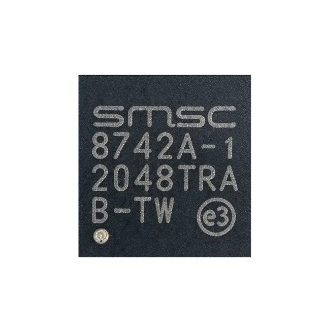
The Microchip LAN8742A-CZ-TR is a low-power 10BASE-T/100BASE-TX Ethernet PHY transceiver with variable I/O voltage, packaged in a 24-pin SQFN (4x4 mm) and supplied on tape and reel. It supports MII and RMII MAC interfaces, operates from a 1.8V to 3.3V variable I/O supply, and is IEEE 802.3 / 802.3u compliant. The device integrates auto-negotiation, auto-polarity correction, and HP Auto-MDIX, eliminating the need for crossover cables. It is well-suited for consumer, embedded, and industrial Ethernet applications. A PHY (physical layer transceiver) is a key element of any Ethernet link: it sits between the MAC controller and the magnetic transformer/RJ-45, handling line encoding/decoding, link training, and electrical signaling over twisted-pair copper. PHY transceivers are part of the broader category of Ethernet interface ICs, which include MAC controllers, switches, and integrated MAC+PHY SoCs. The LAN8742A specifically implements the 10/100 Mbps copper PHY only; higher-speed Gigabit (1000BASE-T) PHYs use multi-level signaling (PAM) and more pins. Key features of the LAN8742A-CZ-TR include Wake-On-LAN support for system-level sleep modes, cable diagnostics for fault detection, and flexPWR flexible power technology for low-power operation. The variable I/O voltage (1.8V-3.3V) allows direct connection to low-voltage MCUs without level shifters. The HP Auto-MDIX feature automatically detects and compensates for TX/RX pair swaps, allowing either straight-through or crossover cables to be used interchangeably. Architecturally, the LAN8742A employs DSP-based echo and crosstalk cancellation to achieve robust 100BASE-TX performance over Cat5 cable. The on-chip PHY includes an integrated termination network and uses energy detect plus power-down modes to meet modern standby-power requirements. MII and RMII MAC interfaces are selectable via strap pins, allowing the same part to be paired with virtually any MCU or SoC MAC. Typical applications include IoT gateways, industrial Ethernet nodes, embedded web servers, building automation controllers, IP cameras, and consumer electronics requiring a wired network connection. The wide 1.8V-3.3V I/O range and low power consumption also make it attractive for battery-powered Ethernet-enabled devices. When designing with the LAN8742A-CZ-TR, follow the Microchip LAN8742 QFN Routing Checklist for proper PCB layout - the analog ground plane and 50-ohm impedance-controlled differential pairs are critical for radiated emissions and signal integrity compliance. Decoupling capacitors must be placed adjacent to each power pin, and the magnetics must be specified to IEEE 802.3 isolation and return-loss specifications. This page synthesizes distributor pricing, drop-in same-BLAN alternatives, and Microchip application-note design notes not found in the manufacturer datasheet alone - giving engineers a single, decision-ready reference.

LAN9115-MT - 10/100 Ethernet Controller, 3.3V | Microchip
The Microchip Technology LAN9115-MT is a single-chip 10/100 Ethernet controller with a nominal 3.3 V supply, clock frequency up to 25 MHz, and a 100-pin TQFP package measuring 14 x 20 mm. It integrates an Ethernet controller and Base-T/TX PHY behind a 16-bit parallel interface for embedded systems requiring medium-performance network connectivity. The device is positioned as a cost-conscious, flexible Ethernet solution that reduces the component count compared with separate controller and physical-layer devices. An Ethernet controller is an interface IC that connects an embedded processor or programmable logic device to a physical Ethernet network. The controller manages higher-level station functions, while the integrated PHY handles the physical signaling required for 10BASE-T and 100BASE-TX links. Within the semiconductor hierarchy, this device is a network interface controller, a communications interface IC, and a system-level Ethernet connectivity component. Verified product information identifies the LAN9115 as a full-featured single-chip 10/100 Ethernet controller intended for 16-bit embedded applications. Its parallel interface supports integration with processors that use a memory-mapped bus rather than a dedicated PCI interface. The supplied distributor classification also identifies a Base-T/TX PHY, while the product description emphasizes price-performance balance for medium-performance requirements. The LAN9115 combines MAC-oriented controller functionality and physical-layer connectivity in one package. This consolidation can simplify PCB routing and reduce the number of external interface components, but the Ethernet magnetics, connector, termination, clock source, decoupling network, and firmware support remain essential parts of a working network subsystem. Its 3.3 V operation also places it in the supply domain of many embedded processors, FPGAs, and industrial controllers. Typical uses include industrial control equipment, embedded gateways, factory data acquisition, instrumentation, building automation, serial-to-Ethernet products, and compact embedded servers. The LAN9115 is most appropriate where 10/100 Ethernet is sufficient and a 16-bit host interface is preferable to a PCI-based architecture. It can also form the network foundation for supervisory systems that exchange configuration, status, and diagnostic data. Board design should reserve careful attention to the 25 MHz clock requirement, 3.3 V power distribution, PHY-to-magnetics routing, and manufacturer-recommended decoupling and layout practices. Because the verified snippets do not provide a complete timing, register, electrical-limit, or absolute-maximum specification set, designers should consult the official manufacturer datasheet before finalizing clock tolerances, impedance, magnetics selection, or software configuration. This page consolidates verified product identity, package, interface, supply, and sourcing information into a practical selection record. It also distinguishes verified facts from unavailable details rather than guessing, while directing engineers to the official datasheet and authorized distributor listings for design validation and current commercial availability.
LAN9117-MD - 10/100 Ethernet Controller | Microchip
The Microchip LAN9117-MD is a high-performance, single-chip 10/100 non-PCI Ethernet controller designed for embedded systems, with a 16-bit CPU interface and integrated Ethernet controller functionality. The verified product information identifies it as a member of the LAN9118 family and emphasizes efficient interfacing with most 16-bit embedded CPUs, low CPU overhead, and suitability for medium- to high-performance applications. It is packaged as an Ethernet interface controller from the LAN9117 family; the exact package designation, pin count, voltage ratings, and full electrical limits require confirmation from the manufacturer datasheet. What is an Ethernet controller? An Ethernet controller is an integrated circuit that manages the hardware and protocol functions required for a host system to communicate over an Ethernet network. In the LAN9117-MD, the 10/100 designation refers to support for 10 Mb/s and 100 Mb/s Ethernet operation, while the non-PCI description identifies its host-side integration approach. The device is intended to reduce CPU involvement in network traffic and simplify embedded Ethernet connectivity. The most important verified feature is the 16-bit host-interface orientation. The product data states that the LAN9117 efficiently interfaces with most 16-bit embedded CPUs and uses a low-CPU-overhead architecture. It also belongs to the LAN9118 family, which provides useful context for firmware and hardware design work involving related SMSC Ethernet controllers. The product is marketed for embedded applications where performance, flexibility, ease of integration, and system-cost control are priorities. LAN9117-MD is suitable for industrial control, embedded instrumentation, network-connected test equipment, and compact embedded platforms that need 10/100 Ethernet without a PCI bus. Compared with a software-heavy network interface, a dedicated Ethernet controller can offload protocol and hardware tasks, reducing the burden placed on the host processor. The actual throughput, media interface, clock requirements, supply voltage, and electrical timing must be checked against the official datasheet before schematic capture. A key design consideration is confirming the exact package footprint and pin compatibility before substituting any part. The available migration guidance explicitly states that the LAN9211 is not a drop-in replacement for the LAN9117 because it uses a different package and requires a new PCB. This distinction is important when comparing Ethernet controllers by function rather than by mechanical interchangeability. This product page consolidates the verified LAN9117-MD role, family information, 10/100 Ethernet capability, 16-bit embedded-CPU interface, sourcing references, and migration cautions into a practical component-selection resource. Numeric electrical limits, pricing, pinout assignments, lifecycle details, and validated drop-in alternatives remain dependent on manufacturer or distributor data.