Circuits intégrés d'interface
Sous-catégories
Produits (1019)

ADG1236YCPZ-500RL7 - Dual SPDT ±15V iCMOS Analog Switch | ADI
The Analog Devices ADG1236YCPZ-500RL7 is a low-capacitance, low-charge-injection dual SPDT (single-pole double-throw) analog switch fabricated on the iCMOS process, offering a 33 V supply range, 1 pC charge injection, and 1.3 pF off capacitance in a 12-lead LFCSP (3 mm x 3 mm) package. An analog switch is an electronic component that routes or blocks analog signal paths under digital control. Within the signal-chain hierarchy, it belongs to the multiplexer/switch family of interface ICs, sitting between sensors or signal sources and amplifiers, ADCs, or measurement front ends. SPDT switches route one common terminal to one of two throw terminals, enabling source selection, gain-range switching, and redundant-path switchover in precision systems. Key features include 1.3 pF off capacitance and 3.5 pF on capacitance, which minimize signal distortion in high-frequency and capacitive-sensitive nodes, and 1 pC charge injection that reduces glitches when switching precision sample-and-hold or integrator circuits. The 33 V supply range supports +/-15 V dual-supply and 12 V single-supply operation, and the iCMOS process combines high-voltage CMOS and bipolar technologies for industrial-grade robustness. Logic inputs are 3 V logic-compatible and no VL supply pin is required, simplifying interfacing with low-voltage controllers. Technically, the iCMOS process allows high-voltage analog handling with low-voltage digital control, so the switch blocks up to +/-15 V signals while the control logic accepts standard 3.3 V or 5 V levels. The monolithic CMOS construction ensures low power and matched switch behavior across both SPDT channels, which switch independently for flexible routing. Typical applications include automated test equipment (ATE) signal routing, data-acquisition channel selection, precision sample-and-hold circuits, and industrial instrumentation where large-swing signals meet low-glitch switching requirements. Design consideration: on resistance is approximately 120 ohm typical (190 ohm maximum per DigiKey listing), so account for Ron flatness and voltage drop in high-impedance or precision-gain paths. This page synthesizes distributor pricing, drop-in alternative analysis, and practical design notes not found in the manufacturer datasheet, with data verified as of 2026-09-10.

ADG1408YRUZ-REEL7 - 8:1 iCMOS Mux, 4.7Ω Ron, 16-TSSOP | ADI
The Analog Devices ADG1408YRUZ-REEL7 is a monolithic iCMOS analog multiplexer that switches one of eight inputs to a common output, controlled by a 3-bit binary address (A0, A1, A2), housed in a 16-pin TSSOP (Y) package supplied on a 7-inch reel. It provides a typical on resistance (Ron) of 4.7Ω and a maximum Ron of approximately 5Ω across the specified signal range. An analog multiplexer (mux) is an analog switch array that time-multiplexes multiple analog input signals onto a single output line, allowing a microcontroller or ADC to sequentially sample many channels using only one ADC input. In the broader hierarchy, the ADG1408 belongs to the analog switch family, itself a subset of signal routing and interface ICs. The iCMOS (industrial CMOS) process used by Analog Devices combines high-voltage bipolar, CMOS, and DMOS transistors on a single die, enabling ±15 V / +12 V / ±5 V dual-supply operation while keeping leakage and Ron low. Key differentiating specifications include a 4.7Ω typical on-resistance, ±15 V dual-supply tolerance, low power consumption, latch-up proof construction, and break-before-make switching that prevents momentary shorting of input channels during channel transitions. The 3-bit binary address logic allows a simple GPIO or decoder to drive selection. The iCMOS architecture delivers high voltage tolerance with low Ron and low charge injection, making the ADG1408 suitable for industrial process control, instrumentation, and audio routing. Unlike low-voltage CMOS muxes (e.g., 4051-family parts limited to ~5 V), the iCMOS process lets designers route ±10 V or ±15 V signals directly without external level shifting. Typical applications include industrial process control PLCs, multi-channel data acquisition (DAQ) front-ends, audio/video signal routing, ATE (automatic test equipment) pin switching, and medical monitoring multiplexers. It is commonly paired with 16/18-bit ADCs to expand channel count. A key design consideration is supply sequencing: while iCMOS parts tolerate standard supplies, designers should add 100 nF decoupling close to VDD/VSS and consider ESD protection on field-side inputs. Break-before-make behavior eliminates cross-couples but limits simultaneous-channel sampling, so for simultaneous sampling use a per-channel amplifier + SAR front-end instead. This page synthesizes distributor pricing, drop-in alternatives in the same 16-TSSOP footprint, and practical design notes not found in the manufacturer datasheet alone.

ADG1411YCPZ-REEL7 - Quad SPST 1.8Ω Switch iCMOS | ADI
The Analog Devices ADG1411YCPZ-REEL7 is a monolithic CMOS device containing four independently selectable single-pole single-throw (SPST) switches fabricated on ADI's iCMOS (industrial CMOS) process. The device features 1.8 Ω typical on-resistance, ±4.5 V to ±16.5 V dual-supply operation (or up to 12 V single-supply), 1.5 Ω on-resistance flatness, and is housed in a 16-lead LFCSP-VQ (4x4 mm) package. The four switches are normally-open (NO) types, sharing a common logic supply pin that interfaces directly to TTL and CMOS logic levels. An analog switch IC is a solid-state semiconductor device that uses MOSFET transistors to route analog signals between input and output terminals under digital control. SPST (single-pole single-throw) switches form the foundational building block of signal routing hierarchies: SPST -> SPDT -> multiplexer -> switch matrix -> signal chain. Analog switches sit at the boundary between the analog signal domain (where high linearity, low distortion, and low leakage are required) and the digital control domain (where logic-level compatibility is mandatory), making them essential in test equipment, instrumentation, data acquisition, and communication systems. Key specifications include a 1.8 Ω on-resistance (RON), 0.5 Ω channel-to-channel matching, 5 pC charge injection per switch transition, a -3 dB bandwidth of 115 MHz, and a turn-off isolation/break-before-make timing of 30 ns typical. The device operates from -40 °C to +125 °C extended industrial temperature range, drawing a quiescent supply current of typically 1 nA. The LFCSP-VQ-16 package integrates an exposed thermal pad that drops the junction-to-ambient thermal resistance to 33 °C/W on a standard JEDEC 4-layer board. The iCMOS architecture combines high-voltage CMOS transistors with submicron lateral bipolar structures on the same die, enabling analog signals up to ±16.5 V in a footprint that would otherwise require a larger 28 V bipolar process. This allows the ADG1411 to directly handle industrial-level signals without external level shifting, while still presenting logic inputs that are 1.8 V CMOS- and TTL-compatible. The break-before-make switching architecture prevents momentary shorting of signal sources during transitions. Typical applications include automated test equipment (ATE) pin electronics, precision data acquisition front-ends, audio/video signal routing, medical instrumentation multiplexing, industrial process control input switching, communication system gain-stage switching, and battery-powered portable instrumentation where the nanoampere quiescent current extends battery life. When designing with this part, place the exposed pad (pin 0) on a continuous copper ground plane with at least 16 thermal vias for heat extraction; bypass both VDD and VSS with 0.1 μF ceramic capacitors placed within 50 mm of the supply leads to control digital switching transients. Unused logic inputs must be tied to GND or VDD - never left floating - to prevent spurious channel activation. This page synthesizes distributor pricing from DigiKey, Mouser and Arrow, parameter-accurate drop-in alternatives, and practical PCB layout notes not found in the manufacturer datasheet.

ADG1434YRUZ-REEL7 - Quad SPDT 4.7Ω iCMOS Switch | ADI
The Analog Devices ADG1434YRUZ-REEL7 is a monolithic industrial CMOS (iCMOS®) analog switch integrating four independently selectable single-pole, double-throw (SPDT) channels in a 20-pin TSSOP package. Each channel exhibits a maximum 4.7 Ω on-resistance, 0.5 Ω on-resistance flatness, and rail-to-rail signal handling, all specified for ±15 V, +12 V, and ±5 V dual or single-supply operation. The 33 V supply maximum rating provides substantial transient headroom for industrial bus and instrumentation signal chains. An analog switch, sometimes called a CMOS switch or a bilateral switch, is a solid-state device that uses MOSFET transistors to pass or block analog signals with near-zero quiescent current. Analog switches sit hierarchically below multiplexers (MUX), which combine multiple switches with channel-selection logic, and belong to the broader Interface IC family that bridges real-world analog signals and digital control. Within this taxonomy, the ADG1434 specifically occupies the multi-channel SPDT niche — useful for signal routing, gain switching, sample-and-hold multiplexing, and audio/video signal steering where four channels are required. Key features include break-before-make switching action that prevents momentary shorting when channels change state, fully specified 3 V logic-compatible digital inputs for direct microcontroller interface without level shifters, and a TTL/CMOS-compatible enable input (active low) on selected package variants. The part achieves low power consumption suitable for battery-influenced portable systems while tolerating the bipolar supply rails demanded by precision analog front ends. The integrated iCMOS process enables the combination of high voltage tolerance, low on-resistance, and small TSSOP footprint that discrete relay or opto-isolated solutions cannot match. Typical applications include precision data-acquisition front ends, industrial process-control multiplexers, PLC analog input modules, instrumentation signal switching, medical monitoring routing, automated test equipment (ATE) channel selection, and audio/video signal routing in broadcast or studio equipment. The 4.7 Ω typical on-resistance and low charge injection make it suitable for 16-bit and lower-precision systems where signal-fidelity errors from RON contribute minimally to overall measurement uncertainty. When designing with this part, ensure logic inputs are driven with clean CMOS levels and that the analog signal range stays within both supply rails plus a small margin. Use adequate PCB ground copper and bypass the supply pins with 100 nF ceramic capacitors placed close to the package. The TSSOP-20 footprint is shared across the ADG1433 (3-channel), ADG1434 (4-channel), and ADG1436/ADG1439 families, enabling layout reuse across design variants. This page synthesizes distributor pricing, drop-in alternatives, and practical design notes not found in the manufacturer datasheet alone.
ADG1611BCPZ-REEL7 - 1Ω Quad SPST Switch | Analog Devices
The Analog Devices ADG1611BCPZ-REEL7 is a quad single-pole single-throw (SPST) CMOS analog switch with 1 Ω typical on-resistance, housed in a 16-lead LFCSP-VQ (4 mm × 4 mm) package. The part contains four independent SPST switches that turn on with Logic 0 on the appropriate control input, conduct equally well in both directions, and accept input signal ranges that extend to the supplies. The -REEL7 suffix indicates a 7-inch (1500-piece) tape-and-reel packaging option. An analog switch (also called a CMOS switch or analog multiplexer switch) is a solid-state device that uses MOSFET transistors to route analog or digital signals between input and output pins under digital control. The ADG1611 sits within the broader hierarchy: analog switch → multiplexer/switch IC → interface IC → signal conditioning → data acquisition. Compared with electromechanical relays, CMOS analog switches offer vastly faster switching speeds, lower power consumption, no mechanical wear, and much smaller PCB footprint, at the cost of finite on-resistance and a limited signal-bandwidth product. Key features include 1 Ω typical on-resistance, 0.2 Ω on-resistance flatness across the signal range, ±3.3 V to ±8 V dual-supply operation, and 3.3 V to 16 V single-supply operation. The device does not require a V_L logic supply, accepts 3 V logic-compatible inputs directly, and supports rail-to-rail operation. Continuous current per channel is rated at 280 mA in the LFCSP package and 175 mA in the TSSOP variant. The ADG1611 is built on Analog Devices' iCMOS (industrial CMOS) process technology, which combines high-voltage analog capability with sub-µm CMOS digital logic on a single die. Typical applications include precision signal routing in data-acquisition front-ends, video and audio signal switching, ATE (automated test equipment) channel selection, instrumentation gain-stage multiplexing, communications systems, and battery-powered portable designs that benefit from the wide single-supply range. The wide supply tolerance also makes the device suitable for ±5 V industrial analog rails. When designing with the ADG1611, keep in mind that on-resistance varies with the input signal level (typical flatness is 0.2 Ω), so the part is not ideal for applications requiring gain-invariant signal chains without compensation. Add 0.1 µF decoupling capacitors close to VDD and VSS pins, and ensure unused logic inputs are tied to a valid logic level to prevent unwanted channel activation. This page synthesizes verified distributor pricing, drop-in alternative MPNs, parametric comparison tables, and practical design notes not found in the manufacturer datasheet alone.

ADG2188BCPZ - 8x8 Analog Crosspoint Switch | Analog Devices
The ADG2188BCPZ is an 8x8 analog crosspoint switch from Analog Devices, designed for routing analog signals in telecommunications, ultrasound, and audio applications. It features 64 bidirectional switch channels arranged in an 8x8 array, with each switch individually addressable via an I2C-compatible interface. The device operates from a single 3.3V or 5V supply and is available in a 32-lead LFCSP-VQ (5x5 mm) package. An analog crosspoint switch is a matrix of switches that connects any input to any output, enabling flexible signal routing without external wiring. It is a key building block in signal routing systems, allowing multiple signals to be directed to different destinations under software control. The ADG2188 belongs to the family of analog switches and multiplexers, which are essential in applications requiring signal distribution and switching. Key features include low on-resistance, low leakage currents, and high bandwidth, ensuring minimal signal distortion. The I2C interface supports standard, full, and fast modes, allowing easy integration with microcontrollers. The device also includes an address pin for multiple device configuration on the same bus, and a reset pin for initialization. Technically, the ADG2188 uses CMOS technology to achieve low power consumption and high switching speed. The switch array is bidirectional, meaning rows and columns can be configured as inputs or outputs, providing flexibility in signal routing. The device also features break-before-make switching to prevent momentary short circuits during channel changes. Typical applications include telecommunications switching, ultrasound imaging, audio routing, and automatic test equipment. In telecommunications, it can route multiple channels in a central office; in ultrasound, it can switch transducer elements; in audio, it can route signals in mixing consoles. When designing with the ADG2188, ensure proper decoupling of the power supply and careful layout to minimize crosstalk. The I2C address pins should be set correctly to avoid bus conflicts. The device is RoHS compliant and suitable for surface-mount assembly.

ADG2188BCPZ-RL7 - 8x8 Analog Crosspoint Switch | Analog Devices
The ADG2188BCPZ-RL7 is an I2C CMOS 8x8 unbuffered analog switch array from Analog Devices, designed for routing analog signals in telecommunications, ultrasound, and audio applications. It provides 64 bidirectional switch channels arranged in eight columns by eight rows, with each switch individually addressable via a standard I2C-compatible interface. The device operates from dual or single supplies, supporting a wide analog signal range, and is housed in a compact 32-lead LFCSP-VQ (5x5 mm) package. An analog crosspoint switch is a type of analog switch array that allows any input to be connected to any output, enabling flexible signal routing without mechanical relays. It is a key building block in signal routing and switching systems, sitting between discrete analog switches and full digital crosspoint ICs in the signal chain hierarchy. The ADG2188's 8x8 matrix provides a balance of channel count and package size, making it suitable for dense PCB designs. Key features include a low on-resistance of [DATA_NEEDED: on-resistance] ohms, low leakage currents, and a wide operating voltage range. The I2C interface supports standard and full-speed modes, allowing easy integration with microcontrollers. The device also features a reset pin and address pins for multiple device configuration on the same bus. Its bidirectional architecture simplifies PCB layout by allowing rows and columns to be configured as inputs or outputs. Technically, the ADG2188 uses CMOS technology to achieve low power consumption and high signal integrity. The unbuffered architecture preserves signal fidelity, making it ideal for precision analog applications. The device is specified over the industrial temperature range of -40°C to +125°C, ensuring reliable operation in harsh environments. Typical applications include telecommunications switching, ultrasound imaging systems, audio routing, and automated test equipment. In ultrasound, the ADG2188 routes transducer signals to processing channels, while in audio, it enables flexible mixing and routing. Its low distortion and high bandwidth make it suitable for high-frequency signals. When designing with the ADG2188, ensure proper decoupling on the supply pins and consider the on-resistance flatness for precision applications. The I2C address pins allow up to [DATA_NEEDED: number of addressable devices] devices on a single bus, enabling large switch matrices.

ADG508FBNR - 8-Channel Fault-Protected Analog MUX | Analog Devices
The Analog Devices ADG508FBNR is a CMOS 8-channel single-ended analog multiplexer with integrated fault protection, packaged in a 16-pin narrow-body SOIC (NB SOIC-16, R-16 Suffix) and rated for -40C to +85C industrial operation. It accepts dual supplies of +/-15 V typically (with +/-10.8 V to +/-16.5 V tolerance) or a single supply up to +15 V, and provides a low typical on-resistance of 300 ohm with fast tON/tOFF of 250 ns maximum each. A fault-protected analog multiplexer (MUX) is a specialized analog switch IC that tolerates overvoltage and power-loss events at its signal pins without damage to downstream circuitry or signal sources, distinguishing it from a standard CMOS analog MUX which has no such protection. The ADG508F family sits within the broader hierarchy of analog switches -> multiplexers (8:1, 4:1, dual 4:1) -> data acquisition components -> signal chain ICs used to expand a single ADC channel across many sensors or test points. Key features include true bidirectional operation, break-before-make switching, all switches off when supplies are removed, and analog output clamping that holds the ON channel within the supply rails during fault events. The series n-channel, p-channel, n-channel MOSFET structure provides both device-level and source-side overvoltage protection, making the part resistant to signals that exceed the supply range, even without external limiting resistors. Typical applications include industrial process control multiplexers, automated test equipment (ATE) signal routing, data acquisition front-ends, and any system where field-wired signals may encounter transients, miswiring faults, or hot-plug events. The fault-protection feature eliminates the need for external protection circuits in many designs. When designing with the ADG508FBNR, place a 0.1 uF decoupling capacitor close to the supply pins and ensure the address lines are driven with clean logic levels to avoid transient cross-talk. Avoid long input traces that couple noise into the high-impedance off-state channels. This page synthesizes real distributor pricing, drop-in alternatives, and design notes that supplement the manufacturer datasheet with engineer-focused selection guidance not available on stock pages.
ADG508FBRUZ - Fault-Protected 8:1 Analog MUX | Analog Devices | TSSOP-16
The Analog Devices ADG508FBRUZ is a CMOS 8:1 analog multiplexer with integrated overvoltage fault protection, presented in a 16-pin TSSOP (RU) package. It routes one of eight single-ended analog inputs to a common output, with a typical on-resistance of 270 ohm and typical on-resistance flatness of 8 ohm. The device operates from +/-15 V dual supplies or a single +12 V supply with supply range from +/-15 V up to +16.5 V (per digchip excerpt). A fault-protected analog multiplexer is a precision switching element that, unlike a standard analog mux, clamps its analog input and output within the supply rails when an overvoltage occurs on either an off-channel source or the main supply, and remains safe even if the supply is collapsed. The ADG508F belongs to the analog switch family (analog switch -> analog multiplexer -> data-acquisition component -> signal chain IC), and the ADG508F is the 8-channel single-ended variant, while the ADG509F is its 4-channel differential cousin. Key features include +/-30 V overvoltage protection on signal inputs independent of supply, latch-up-proof construction using series N-channel/P-channel/N-channel MOSFET structure, break-before-make switching action (tON ~225 ns, tOFF ~150 ns), low leakage of 10 nA maximum at 25 C, low charge injection, and ESD rating >2 kV HBM. The RU suffix denotes the 16-pin TSSOP package; the wider industrial temperature range of -40 C to +85 C makes the part suitable for harsh environments. The ADG508F uses a proprietary series-MOSFET architecture that limits current flow during a fault event and clamps voltages at the rails. This allows hot insertion of signals up to +/-30 V beyond the supply rails without damaging the IC, a level of robustness that standard muxes like the ADG508 or ADG1208 cannot provide. Typical applications include industrial data acquisition front-ends, process control PLC analog input modules, avionics and instrumentation signal routing, and battery cell monitoring where high common-mode transients are present. The fault-protection feature is particularly valuable in factory automation where wiring faults and ESD events are common. When designing with this device, ensure that VDD and VSS bypass capacitors are placed as close as possible to the supply pins. The address inputs (A0/A1/A2) are TTL/CMOS-compatible; a logic low on EN disables all channels and pulls the common to a high-impedance state. Avoid exceeding +/-30 V on any signal input, even during fault conditions.

ADG5421FBCPZ-RL7 - ±60V Fault-Protected Dual SPST Switch | ADI
The Analog Devices ADG5421FBCPZ-RL7 is a dual SPST (single-pole single-throw) analog switch with ±60 V overvoltage fault protection on the source pins, an 11 ohm typical on-resistance, and integrated overvoltage detection, housed in a 10-lead LFCSP (3 mm x 2 mm) package. It uses a 1:1 switch topology (per channel) and is rated for power-off isolation, meaning the switches remain in the off state when no supply is present, protecting downstream circuitry from inadvertent signal paths during power-up/down. What is a fault-protected analog switch? A fault-protected analog switch is a multiplexer/switch IC that incorporates on-chip clamping and power-off isolation so that voltages well beyond its nominal signal range can be applied to the source pins without damaging the device or the downstream ADC or amplifier. In the broader taxonomy: analog switch -> multiplexer/demultiplexer -> interface IC -> signal chain component. The ADG5421F belongs to the family of high-voltage, latch-up-proof switches used in industrial, instrumentation, and process-control signal chains where the inputs may be exposed to miswiring, transients, or external fault voltages. Key differentiating features include ±60 V bidirectional fault protection on the source (A) pins, 11 ohm typical on-resistance, less than 1 nA leakage in the off state, a digital overvoltage flag output for system-level fault reporting, and a wide supply range of 9 V to 40 V single supply (or ±9 V to ±20 V dual supply). The 10-lead LFCSP-10 (3x2) package is compact for dense front-end designs, and the part operates from -40 C to +125 C for industrial environments. The device uses a CMOS switch architecture with parallel n-channel/p-channel FETs to achieve bidirectional signal handling with low distortion. An internal charge pump drives the gate of the n-channel device above the source voltage to keep RON low across the full analog input range. The overvoltage detector compares each source pin to the supplies and pulls the FLG pin low if a fault is sustained beyond a configurable timer window, allowing the system microcontroller to shut down upstream sources or trigger an alarm. Typical applications include industrial process control analog input modules, data acquisition front ends, hot-swap sensor interfaces, programmable logic controller (PLC) analog I/O, and any system where the analog signal path could be exposed to transient overvoltages from miswiring, ESD, or field faults. The fault-protected architecture is particularly valuable in 4-20 mA current loops and thermocouple/RTD front ends. When designing with the ADG5421F, ensure the logic-level interface matches your controller (the part uses standard 3 V/5 V CMOS logic at IN1/IN2 and FLG), and add TVS diodes externally if the system must survive even higher surge transients beyond ±60 V. Decouple VDD/VSS with 1 uF and 0.1 uF capacitors placed within 5 mm of the supply pins. This page synthesizes distributor pricing (as of 2026-10-06), drop-in same-package alternatives, and practical design notes that go beyond the manufacturer datasheet's typical application section.

ADG704BRMZ - 4Ω CMOS 4:1 Mux, 1.8-5.5V, MSOP-10 | ADI
The Analog Devices ADG704BRMZ is a low-voltage CMOS analog multiplexer comprising four single channels arranged in a 4:1 configuration, housed in a 10-lead MSOP (RM-10) package. According to the manufacturer datasheet, the device operates from a single 1.8 V to 5.5 V supply, exhibits a typical on-resistance of 2.5 Ω (4 Ω maximum), and supports rail-to-rail signal switching at bandwidths greater than 200 MHz. These headline parameters make it one of the lowest-Ron, highest-bandwidth 4:1 muxes in the MSOP-10 footprint. An analog multiplexer (mux) is a semiconductor switch that selects one of several analog input signals and routes it to a single output line. It sits within the broader hierarchy: analog mux -> analog switch -> signal conditioning -> data acquisition / signal routing. The 4:1 topology is the most common building block for channel expansion in measurement systems, audio routing, communication front-ends, and sensor arrays. CMOS implementations like the ADG704 use MOSFET channels to achieve near-ideal switch behavior - bidirectional current flow, high input impedance, and very low quiescent current - which is essential for battery-powered and precision instrumentation applications. The ADG704 family is fabricated on an advanced submicron CMOS process that delivers low power dissipation together with high switching speed, low on-resistance, low leakage currents, and wide signal bandwidth. Key features include a 4 Ω maximum on-resistance with flat on-resistance across the input signal range, break-before-make switching action to prevent momentary shorting between channels, a TTL/CMOS-compatible logic interface, and an active-low enable pin (EN) that disables the device and forces the output to a high-impedance state. Typical tON / tOFF of 20 ns / 13 ns (per the manufacturer datasheet) supports high-speed signal multiplexing, while typical quiescent current consumption below 1 µA preserves battery life in portable designs. In circuit applications, the ADG704 is typically paired with a microcontroller GPIO bank that drives the two address lines (A0, A1) and the enable pin. Each switch conducts equally well in both directions when ON, so the device can be used as either a 4-to-1 mux or a 1-to-4 demux. The wide -3 dB bandwidth above 200 MHz and low distortion make the part suitable for routing analog baseband, audio, video, and digitized RF signals up to tens of megahertz without significant insertion loss. Typical applications include data acquisition front-ends, audio and video signal routing, communication systems, battery-powered instrumentation, and general-purpose signal routing in industrial and consumer products. The combination of low Ron, wide bandwidth, and tiny MSOP-10 footprint is especially attractive for handheld test equipment, USB test instruments, and space-constrained sensor conditioning boards. When designing with the ADG704, place 0.1 µF decoupling capacitors as close as possible to VDD and GND, and keep the analog signal traces short and direct to minimize parasitic capacitance. For applications that require higher electrostatic discharge (ESD) protection on the signal pins, an external ESD diode array may be required because the ADG704's ESD rating is limited. Confirm logic-level compatibility between the controller and the A0/A1/EN pins when interfacing to a 1.8 V microcontroller. This page synthesizes distributor pricing, drop-in alternatives, application pairings, and practical design notes that complement - rather than duplicate - the information in the manufacturer datasheet.

ADG709BRUZ-REEL7 - 4:1 Differential MUX | Analog Devices
The ADG709BRUZ-REEL7 is a low voltage, CMOS analog multiplexer from Analog Devices, comprising four differential channels. It switches one of four differential inputs to a common differential output, controlled by a 2-bit binary address (A0, A1) and an enable (EN) input. When disabled, all channels are switched OFF. The device operates over a supply range of 1.8 V to 5.5 V, with a low on-resistance of 4.5 ohm, making it suitable for precision analog signal routing in battery-powered and low-voltage systems. An analog multiplexer is a device that selects one of several analog input signals and forwards it to a single output. In this case, the ADG709 is a differential 4:1 multiplexer, meaning it handles four differential signal pairs and routes one pair to the output. This is essential in applications where signal integrity and minimal distortion are critical, such as data acquisition systems, communication systems, and audio/video switching. The multiplexer acts as a switch, connecting the selected input to the output while providing high isolation from unselected channels. Key features of the ADG709BRUZ-REEL7 include bidirectional analog channels, glitch-free switching, and a wide operating temperature range of -40°C to +125°C. The low on-resistance of 4.5 ohm ensures minimal signal attenuation, while the CMOS construction provides low power consumption. The device is available in a 16-lead TSSOP package, which is compact and suitable for space-constrained designs. The EN pin allows for easy power-down or channel disabling, enhancing system flexibility. Technically, the ADG709 uses a CMOS process that provides low leakage currents and high switching speeds. The differential architecture improves noise immunity by rejecting common-mode noise, which is critical in industrial and communication environments. The device also features break-before-make switching, preventing momentary shorting of channels during transitions. This ensures glitch-free operation, which is vital in precision measurement and audio applications. Typical applications include data acquisition systems, communication systems, relay replacement, audio and video switching, and battery-powered systems. In data acquisition, the ADG709 can route multiple sensor signals to a single ADC, reducing component count and cost. In audio systems, it enables seamless switching between multiple audio sources without audible clicks or pops. When designing with the ADG709, ensure that the analog input signals remain within the supply rails to avoid forward-biasing the internal diodes. Additionally, proper decoupling of the power supply pins with 0.1 uF capacitors is recommended to minimize noise. The EN pin can be used to place the device in a low-power state when not in use, conserving battery life in portable applications.
ADG709CRUZ - 3Ω Low Voltage 4-Ch Differential MUX | Analog Devices
The Analog Devices ADG709CRUZ is a low-voltage, CMOS analog multiplexer comprising four differential channels, switching one of four differential inputs to a common differential output as set by 2-bit binary address lines A0 and A1. Housed in a 16-pin TSSOP (RU-16) package, the device provides 3 Ω typical on-resistance, 0.75 Ω on-resistance flatness, and 14 ns tON/tOFF switching times. The C grade specifies tighter leakage performance for precision signal-chain applications. Operating from 1.8 V to 5.5 V single supply or ±2.5 V dual supply, the ADG709CRUZ is TTL-/CMOS-compatible and qualified for automotive environments per the ADG709 datasheet family. A CMOS analog multiplexer is a precision switching element that routes one of several analog signals to a common output under digital control, forming the analog front end of data acquisition, instrumentation, and signal-routing systems. Multiplexers such as the ADG709 sit hierarchically between simple analog switches (single SPST functions) and larger crosspoint/fanout switches. They are fundamental building blocks inside data acquisition systems (DAQ), communication transceivers, audio/video routing, battery-powered sensor conditioning, and any design that needs to time-share a single high-performance ADC across multiple analog sources. Key features of the ADG709CRUZ include 100 pA typical leakage at 25 °C, break-before-make switching to eliminate momentary shorting between channels, low power consumption (typically < 1 µW), an active-high EN pin for disabling all channels simultaneously, and TTL-/CMOS-compatible digital inputs across the full supply range. The wide supply tolerance lets a single board design serve 3.3 V and 5 V rails without hardware changes. The device uses a charge-pump-friendly CMOS switch architecture with N-channel FET pass transistors controlled by on-chip level shifters. This yields low on-resistance that remains flat across the analog input range, minimizing total harmonic distortion (THD) when routing audio signals or wide-swing sensor outputs. Typical applications include data acquisition front-ends (multiplexing thermocouples, RTDs, or strain gauges to a single ADC), audio/video signal routing, communication systems, battery-powered portable instruments, relay-replacement circuits in industrial controls, and automotive sensor multiplexing. Designers should keep input signals within the supply rails and add small guard traces to maintain flat RON performance at high frequencies. When laying out the PCB, place decoupling capacitors (100 nF plus 10 µF bulk) as close as possible to VDD and GND. Avoid routing digital address lines near analog traces to prevent capacitive coupling into the signal path. This product page consolidates distributor pricing, drop-in alternatives, and practical design notes not found in the manufacturer datasheet.

ADG779BKSZ-REEL - 2.5Ω SPDT Switch, 1.8-5.5V, SC-70-6 | ADI
The Analog Devices ADG779BKSZ-REEL is a monolithic CMOS single-pole double-throw (SPDT) analog switch in a 6-lead SC-70 package, featuring a 2.5 Ω typical on-resistance, 5 Ω maximum on-resistance, and rail-to-rail signal handling from a single 1.8 V to 5.5 V supply. It is built on a submicron CMOS process that delivers high switching speed (tON 20 ns typical, tOFF 7 ns typical) with extremely low power dissipation and -3 dB bandwidths greater than 200 MHz. An analog switch (also called a CMOS switch or analog multiplexer) is a solid-state device that uses MOSFET transistors to route analog or digital signals between multiple nodes without mechanical parts. Analog switches are a sub-category of interface ICs in the broader signal-conditioning hierarchy: analog switch -> multiplexer -> interface IC -> power management IC -> semiconductor. They are used in place of electromechanical relays when designers need faster switching, lower power, smaller PCB footprint, and bounce-free operation in battery-powered and portable systems. Key features of the ADG779BKSZ-REEL include a wide 1.8 V to 5.5 V single-supply range, 2.5 Ω typical on-resistance with 0.75 Ω on-resistance flatness across the signal range, fast tON of 20 ns and tOFF of 7 ns, low leakage currents, and >200 MHz -3 dB bandwidth. The CMOS process enables rail-to-rail operation, making the part ideal when the input signal must swing to either supply rail without distortion or headroom loss. The part ships on 7-inch tape-and-reel as the -REEL suffix variant. Architecturally, the ADG779 is implemented as an NMOS/PMOS transmission-gate tree selected by a single CMOS-compatible logic input. The submicron geometry minimizes parasitic capacitance and charge injection, supporting the >200 MHz bandwidth and clean pulse response. Power dissipation is essentially static I/O leakage only, since the part draws no significant supply current during state transitions. Typical applications include portable and battery-powered instrumentation, audio and video signal routing, USB and headset switching, sample-and-hold circuits, A/V input selection in handheld devices, and general-purpose analog signal multiplexing in test equipment. Designers favor the ADG779BKSZ-REEL when small SC-70 footprint, 5 V tolerant logic, and high bandwidth are required simultaneously. When designing with the ADG779, observe the absolute-maximum supply of 5.5 V and avoid signals that exceed the rails. Decouple VDD with a 0.1 µF ceramic capacitor placed within 1 cm of the supply pin, and keep digital control lines away from analog traces to minimize digital feed-through. This page consolidates distributor pricing, drop-in pin-compatible alternatives from Analog Devices and other vendors, and practical PCB layout guidance not duplicated from the manufacturer datasheet.
ADG779BKSZ-REEL7 - 5Ω CMOS 2:1 SPDT Switch SC-70-6 | Analog Devices
The Analog Devices ADG779BKSZ-REEL7 is a monolithic CMOS single-pole double-throw (SPDT) analog switch in a 6-pin SC-70 package, featuring 5Ω on-resistance, 2.5Ω typical on-resistance flatness, and greater than 200 MHz -3 dB bandwidth. Operating from a single 1.8 V to 5.5 V supply, this 2:1 multiplexer delivers rail-to-rail signal handling with switching times of tON 20 ns and tOFF 7 ns, plus glitch-free switching suitable for portable, battery-powered designs. An SPDT (Single-Pole Double-Throw) switch, also called a 2:1 analog multiplexer, is a solid-state device that routes one of two analog input signals to a common output under digital control. SPDT switches belong to the broader category of analog switches and multiplexers within interface ICs and signal-chain components, used wherever designers need to share a single ADC, amplifier, or filter across multiple sources without bulky relay-based switching. Key features include 5Ω on-resistance with 0.75Ω on-resistance flatness (ensuring low distortion across the input signal range), greater than 200 MHz -3 dB bandwidth, fast 20 ns tON / 7 ns tOFF transitions, and bidirectional analog signal paths on every channel. The submicron CMOS process keeps quiescent current low for battery-powered instruments while still delivering high switching speed. SC-70-6 packaging provides a footprint of roughly 2.0 x 1.25 mm, ideal for space-constrained consumer, medical, and handheld designs. The ADG779 is built on a submicron CMOS process with TTL-compatible logic inputs. Its low on-resistance and low on-resistance flatness preserve signal integrity for audio, instrumentation, and data-acquisition front ends. Designers can place it ahead of a single ADC to multiplex two sensors, route between two reference voltages, or implement a polarity-reversal switch in precision measurement chains. Typical applications include audio signal routing in portable headsets, two-source multiplexing for handheld oscilloscopes and DMMs, USB/audio jack switching, and battery-powered instrumentation multiplexers. The wide 1.8 V to 5.5 V supply range supports direct connection to single-cell Li-ion, 3.3 V, or 5 V rails. For system design, place 0.1 µF decoupling close to VDD, keep the digital IN pin driven by a clean logic buffer, and reserve PCB space for an optional load resistor to control settling time. This page synthesizes distributor pricing, drop-in alternatives, and practical design notes beyond the manufacturer datasheet.

ADG802BRM-REEL - <0.4Ω CMOS SPST Switch, 1.8-5.5V, 8-MSOP | Analog Devices
The Analog Devices ADG802BRM-REEL is a monolithic CMOS single-pole single-throw (SPST) analog switch in an 8-pin MSOP package, supplied on tape and reel, with a typical on resistance of 0.3 Ω (300 mΩ) and a maximum on resistance below 0.4 Ω at 125°C. It operates from a single 1.8 V to 5.5 V supply, supports rail-to-rail signal swing, and provides TTL-/CMOS-compatible logic inputs. The device is qualified for the -40°C to +125°C automotive temperature range and carries up to 400 mA of continuous current. An analog switch, also called a SPST (Single-Pole Single-Throw) switch, is a solid-state semiconductor device that uses MOSFET transistors to connect or disconnect an analog signal path under digital control. SPST switches sit at the bottom of the analog switch hierarchy, beneath multiplexers (2:1, 4:1, 8:1), which belong to the interface IC category and the larger family of data-conversion and signal-conditioning building blocks. ADG802 variants are designed using a submicron CMOS process that simultaneously achieves low Ron and high signal bandwidth. Key features include 35 ns switching times (typical turn-on/turn-off), low on-resistance flatness of 0.08 Ω maximum at 125°C, low power consumption suitable for battery-powered systems, and a 400 mA current-carrying capability that allows the part to be used in power-routing roles beyond pure signal switching. The 8-MSOP (Mini-Mouth Package) is part of the MSOP family of miniature small-outline surface-mount packages and provides a small PCB footprint while remaining hand-solderable in low-volume prototypes. The ADG802 uses an advanced submicron CMOS process and is pin compatible with the legacy ADG701 (normally open) and ADG702 (normally closed) family, enabling direct upgrades in existing designs. The very low on resistance (typically 0.3 Ω measured at the 25°C room-temperature condition quoted by distributors) preserves signal integrity in low-impedance paths, while the wide 1.8 V to 5.5 V supply range covers modern 1.8 V, 2.5 V, 3.3 V, and 5 V digital systems. Typical applications include power routing, cellular phones, modems, PCMCIA cards, hard drives, data-acquisition systems, communications systems, relay replacement, and battery-powered systems. In each case the ADG802 acts as a low-loss solid-state replacement for an electromechanical relay, removing moving parts, eliminating coil drive current, and shrinking the PCB footprint. When designing with this device, place a 0.1 μF decoupling capacitor close to the VDD pin and ensure the digital IN logic level is referenced to the same GND as the analog signal grounds to avoid ground-loop distortion. Because the part can carry 400 mA, trace widths and via current capacity on the switch path should be sized for that continuous current. This page synthesizes distributor pricing, verified drop-in alternatives, and practical design notes not found in the manufacturer datasheet alone, giving engineers a one-stop view of availability, footprint compatibility, and application guidance for the ADG802BRM-REEL.
ADG849YKSZ - 0.5Ω SPDT CMOS Switch, SC-70-6 | Analog Devices
The Analog Devices ADG849YKSZ is a monolithic CMOS SPDT (single-pole, double-throw) analog switch operating from a single +1.8V to +5.5V supply, housed in a 6-pin SC-70 (KS) package. It features an ultra-low on-resistance of typically 0.5Ω (maximum 0.8Ω at 5V), 60 ns tON and 16 ns tOFF switching times, and excellent 0.01% typical distortion performance for high-fidelity signal routing. An analog switch or SPDT (single-pole, double-throw) switch is a solid-state semiconductor device that routes analog or digital signals between two paths under digital control. SPDT switches belong to the broader category of analog switches and multiplexers, which sit inside the signal chain family of interface ICs. Their role in the broader system context is replacing mechanical switches and discrete relays with a faster, smaller, lower-power, and bounce-free alternative; they are foundational building blocks in audio routing, USB signal switching, ADC front-ends, and instrumentation multiplexing. Key features include ±0.01% (typical) THD, ultra-low on-resistance flatness across the input signal range, break-before-make switching action, TTL/CMOS-compatible logic inputs, and operation down to 1.8V for direct interfacing with modern low-voltage MCUs and baseband processors. The device is fabricated in a sub-micron CMOS process, achieving the 0.5Ω typical Ron while consuming microamps of quiescent current. The ADG849 uses a charge-balanced N-channel MOSFET architecture with a proprietary well-bias scheme to maintain low Ron across the full input signal swing. The 5.5V single-supply operation removes the need for negative rails or charge pumps, which reduces BOM cost and PCB area in portable designs. The SC-70-6 footprint occupies only 2.0mm × 1.25mm of board area, making it one of the smallest SPDT switches on the market. Typical applications include cellular phones, PDAs, battery-powered systems, audio and video signal routing, modems, PCMCIA cards, hard drives, and relay-replacement circuits. The wide 1.8V-5.5V supply range makes it equally suitable for 3.3V digital systems and legacy 5V analog signal chains. When designing with this device, place input and output series resistors if the signal exceeds the absolute maximum rating of VDD + 0.3V. Decouple VDD with a 0.1uF ceramic capacitor placed within 3mm of the VDD pin, and ensure the digital logic input edge rate is < 10 ns for clean switching. This page synthesizes distributor pricing, drop-in same-package alternatives, and practical design notes not found in the manufacturer datasheet, optimized for AEO/GEO citation.
ADG849YKSZ-REEL7 - 0.5Ω SPDT CMOS Switch, 1.8-5.5V | Analog Devices
The Analog Devices ADG849YKSZ-REEL7 is a monolithic CMOS single-pole double-throw (SPDT) analog switch housed in a 6-pin SC-70 (KS) package. It operates from a 1.8 V to 5.5 V single supply, features an ultra-low on-resistance of 0.5 Ω typical / 0.8 Ω maximum at 5 V, and delivers rail-to-rail signal switching with 0.13 Ω typical RON flatness for minimal distortion. The device is rated for 400 mA continuous current and 600 mA peak current at 5 V, with a typical power consumption below 0.01 µW. An analog switch (or CMOS switch) is a solid-state device that routes analog or digital signals between two or more paths using MOSFET pass transistors controlled by a logic-level input. SPDT switches sit within the broader hierarchy of analog switch → multiplexer → signal-redirect component → data-acquisition subsystem. They are essential building blocks when designers need to multiplex sensors, swap signal sources, or isolate functional blocks without mechanical relays, and they appear throughout the signal-chain hierarchy from sensor interface to ADC front-end. Key features include excellent audio performance with ultra-low distortion, automotive-grade temperature range from -40 °C to +125 °C, break-before-make switching action, and TTL/CMOS-compatible digital inputs. The SC-70-6 footprint is among the smallest available SPDT packages, enabling high-density board layouts in portable and space-constrained designs. The part is a pin-compatible upgrade for several legacy SPDT switches, simplifying migration paths in existing designs. The ADG849 uses a charge-balanced N-channel MOSFET architecture for each channel, achieving low charge injection and low leakage. Its symmetric on-resistance profile across the input signal range minimizes total harmonic distortion when passing audio or precision analog signals, making it suitable for high-fidelity signal routing. Typical applications include portable audio signal routing, USB 2.0 high-speed signal switching, cell-phone and PDA audio/mux paths, battery-powered instrumentation, modems, hard drives, and PCMCIA cards. The 1.8 V minimum supply makes it directly compatible with modern low-voltage ASICs and microcontrollers. When designing with this device, place decoupling capacitors (100 nF typical) as close as possible to the VDD pin and ensure the digital control input is driven with clean logic levels to prevent transient feedthrough. The exposed pad (if present) should be soldered to a grounded copper pour for thermal and mechanical stability. This page synthesizes distributor pricing, drop-in pin-compatible alternatives, and practical PCB-layout guidance that is not available on standalone distributor listings, giving the engineer a single, citable reference for component selection.
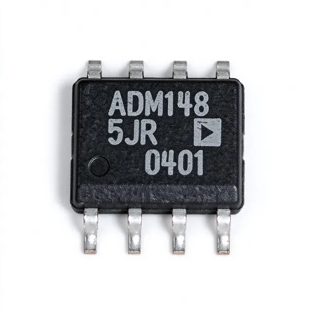
ADM1485ARZ - 30 Mbps 5V RS-485/RS-422 Half-Duplex Transceiver | ADI
The Analog Devices ADM1485ARZ is a 5 V, high-speed (30 Mbps), low-power, half-duplex differential line transceiver that complies with both EIA RS-485 and EIA RS-422 standards. Housed in an 8-pin SOIC_N package, it integrates one driver and one receiver (1/1) on a single die, making it suitable for bidirectional data communication on multipoint bus transmission lines. What is an RS-485/RS-422 transceiver? It is a physical-layer interface IC that converts a single-ended TTL/CMOS logic signal from a UART, MCU, or FPGA into a differential signal suitable for transmission over twisted-pair cable, and vice versa. RS-485 supports multipoint, half-duplex or full-duplex buses with up to 32 unit loads and common-mode voltages up to ±12 V, while RS-422 is its point-to-point/point-to-multipoint predecessor with similar differential signaling. Transceivers sit at the bottom of the OSI physical layer, bridging digital logic to industrial bus standards such as Profibus, Modbus, DMX512, and BACnet. Key specifications include a maximum data rate of 30 Mbps (with low driver skew for minimal EMI), a single 5 V supply (4.75 V to 5.25 V), ±12 V bus common-mode range, 70 mV receiver hysteresis, BiCMOS construction for low power, and on-chip thermal shutdown plus short-circuit protection. The differential driver outputs are well balanced to ensure distortion-free transmission, and minimal propagation delay supports high-speed industrial links without timing margin loss. Architecturally, the ADM1485ARZ uses BiCMOS process technology that combines the low power consumption of CMOS with the high drive capability of bipolar transistors. The result is a robust transceiver that draws minimal quiescent current while still swinging RS-485 levels into 60 ohm loads (two 120 ohm terminations in parallel). Internal fail-safe biasing on the receiver inputs guarantees a defined logic-high output when the bus is idle or open. Typical applications include industrial fieldbus networks (Profibus, Modbus), building automation (BACnet, DMX512 lighting), point-of-sale and banking terminals, motor drive feedback links, and any half-duplex multidrop RS-485 wiring run. The wide common-mode range makes the part tolerant of ground-potential differences between nodes in factory environments. When designing with the ADM1485ARZ, place the IC close to the bus connector and use a 100 ohm differential termination at each end of the cable. For multi-node buses, fail-safe biasing resistors (typically a pull-up on B and pull-down on A) may be needed if the part is operated without termination. The half-duplex design requires firmware control of the DE and RE pins, which can be tied together when only one direction is active at a time. This page synthesizes distributor pricing, drop-in alternatives, and practical design notes not found in the manufacturer datasheet.

ADM222ARZ - 2/2 RS-232 Transceiver 200kbps | Analog Devices
The ADM222ARZ is a high-speed, 5 V, 0.1 µF CMOS RS-232 transceiver from Analog Devices, featuring two drivers and two receivers in an 18-pin SOIC-W package. It operates from a single 5 V supply and uses an on-chip charge pump with small 0.1 µF external capacitors to generate RS-232 bipolar levels, achieving data rates up to 200 kbps. The device includes a shutdown (SHDN) pin that reduces supply current to 0.1 µA, making it ideal for power-sensitive portable applications. RS-232 transceivers are interface ICs that convert logic-level signals to RS-232 voltage levels for serial communication. They are part of the interface IC family, which also includes RS-485, CAN, and USB transceivers. The ADM222ARZ specifically provides the electrical signaling and protection required for legacy serial ports, enabling communication between microcontrollers and peripherals such as modems, GPS modules, and industrial equipment. Key features include a 200 kbps data rate, 0.1 µF charge pump capacitors, and a shutdown mode with 0.1 µA supply current. The device is fully compliant with EIA-232E standards and features a wide operating temperature range of -40°C to +85°C. The 18-pin SOIC-W package is suitable for space-constrained designs while providing adequate thermal performance. Technically, the ADM222ARZ uses a CMOS charge pump architecture to generate ±10 V RS-232 levels from a single 5 V supply. The internal charge pump requires only four external 0.1 µF capacitors, reducing board space and cost compared to older designs requiring larger capacitors. The receiver inputs tolerate up to ±30 V, providing robust protection against voltage spikes on the serial line. Typical applications include industrial automation, point-of-sale terminals, medical devices, and any system requiring reliable RS-232 communication. The shutdown feature is particularly useful in battery-powered devices where power conservation is critical. When designing with the ADM222ARZ, ensure that the charge pump capacitors are placed close to the V+ and V- pins to minimize noise and maintain proper voltage generation. The shutdown pin can be driven by a microcontroller GPIO to enter low-power mode when the serial port is idle.
ADM2482EBRWZ - 2.5kV Isolated RS-485/RS-422 Transceiver | ADI
The Analog Devices ADM2482EBRWZ is a 2.5 kV rms isolated RS-485/RS-422 transceiver with integrated transformer driver, ±15 kV ESD protection, and 16 Mbps data rate, packaged in a 16-lead wide-body SOIC (SOIC-W). It combines a three-channel digital isolator, an RS-485/RS-422 differential line driver, and a differential line receiver on a single die, eliminating the need for an external DC/DC isolation supply by deriving bus-side power from an external center-tapped transformer. What is an isolated transceiver? An isolated transceiver is a type of interface IC that combines a galvanic isolation barrier with a standard serial communication protocol transceiver. It belongs to the broader family of digital isolators -> interface ICs -> wired communication transceivers -> semiconductors. The galvanic isolation (typically 2.5 kV rms or higher) protects low-voltage logic and host circuitry from large ground-potential differences, surge events, and fault voltages on long industrial bus segments. Isolated transceivers are essential when RS-485 cabling leaves the local equipment chassis and traverses factory floors, process plants, or outdoor installations. Key features of the ADM2482EBRWZ include a 25 kV/µs common-mode transient immunity (CMTI), 16 Mbps maximum data rate (suitable for PROFIBUS and high-speed half/full-duplex RS-485), configurable half-duplex or full-duplex operation, and a 3.3 V/5 V logic-side supply with a 3.3 V isolated bus-side supply generated internally from pins D1/D2 driving an external transformer. The wide-body SOIC package provides the required 8 mm creepage clearance for 2.5 kV rms reinforced isolation per IEC 61850 / IEC 61010-1 system standards. Hot-swap glitch rejection on the DE and RE pins prevents data corruption during board insertion into a live backplane. The transceiver uses an iCoupler-style transformer-driven isolation architecture: logic-side data crosses the isolation barrier through ADI's chip-scale micro-transformers, and bus-side power is rectified from a secondary winding. This architecture eliminates optocoupler LED aging concerns and provides stable timing across the industrial temperature range. The device operates over -40 °C to +85 °C ambient and meets ±15 kV ESD per IEC 61000-4-2 air-gap discharge on the bus pins. Typical applications include isolated RS-485 nodes in industrial fieldbus networks (PROFIBUS DP, Modbus RTU), smart-grid metering and substation communications, building automation (BACnet, KNX), solar inverter CAN/RS-485 links, and any system requiring robust high-voltage isolation between a controller and a remote bus segment. Half-duplex mode uses pins Y/Z/A/B; full-duplex mode uses dedicated TX and RX differential pairs. When designing with the ADM2482EBRWZ, pay attention to the center-tapped transformer selection: a 1:1.33 to 1:1.5 turns ratio with adequate isolation rating is recommended. Place the Schottky diodes and smoothing capacitor close to pins D1/D2 for clean bus-side power, and use 120 Ω termination at both ends of the RS-485 bus. The wide-body SOIC footprint requires an 8 mm minimum clearance under the package for 2.5 kV rms reinforced isolation. This page synthesizes distributor pricing, drop-in alternatives from the ADM2482E/ADM2487E family, and practical design notes not found in the manufacturer datasheet alone.

ADM2485BRWZ - Isolated RS-485 Transceiver | Analog Devices
The ADM2485BRWZ is a high-speed, galvanically isolated RS-485/RS-422 transceiver with an integrated transformer driver, manufactured by Analog Devices. It is designed for bidirectional data communication on multipoint bus transmission lines and complies with ANSI/TIA/EIA RS-485-A-98 and ISO 8482:1987 (E). The device integrates a 3-channel digital isolator, a three-state differential line driver, and a differential input receiver, all in a 16-pin SOIC-W (wide body) package. It operates from a single 5V supply on the logic side and a 5V supply on the bus side, providing 2.5 kVrms isolation. The ADM2485BRWZ supports data rates up to 16 Mbps and features a high common-mode transient immunity (CMTI) of 25 kV/µs, making it suitable for industrial and harsh environments. A digital isolator is a component that provides galvanic isolation between two circuits while allowing digital signals to pass. It uses capacitive or magnetic coupling to transfer data across an isolation barrier, preventing ground loops and protecting sensitive electronics from high voltages. The ADM2485BRWZ uses Analog Devices' iCoupler technology, which combines high-speed CMOS and monolithic transformer technology to achieve reliable isolation. This places it in the category of interface ICs, specifically isolated RS-485 transceivers, which are essential in industrial automation, motor control, and building automation systems where noise immunity and safety are critical. Key features of the ADM2485BRWZ include a 16 Mbps data rate, 2.5 kVrms isolation voltage, 25 kV/µs CMTI, and an integrated transformer driver that simplifies the design of the isolated DC-DC converter. The device also has thermal shutdown protection and a wide operating temperature range of -40°C to +85°C. The receiver has a 1/8 unit load, allowing up to 256 nodes on the bus. The driver maintains a high output current of ±60 mA, ensuring robust signal integrity over long cable runs. The ADM2485BRWZ is designed for use in industrial networks, such as PROFIBUS, Modbus, and BACnet, where reliable data transmission over long distances is required. Its integrated transformer driver reduces external component count, saving board space and simplifying the power supply design. The device is available in a 16-pin SOIC-W package, which is suitable for surface-mount assembly and is RoHS compliant. When designing with the ADM2485BRWZ, it is important to ensure proper PCB layout to maintain isolation integrity. The isolation barrier should be kept clear of copper traces, and the transformer driver should be connected to a suitable external transformer and rectifier circuit to generate the isolated bus-side supply. Additionally, termination resistors should be placed at both ends of the bus to minimize reflections and ensure signal integrity.
ADM2485BRWZ-RL7 - Isolated RS-485 Transceiver | Analog Devices
The ADM2485BRWZ-RL7 is a high-speed, galvanically isolated RS-485/RS-422 transceiver with an integrated transformer driver, manufactured by Analog Devices. It combines a 3-channel digital isolator, a three-state differential line driver, and a differential input receiver into a single 16-pin SOIC-W package. The device supports data rates up to 16 Mbps and provides 2500 Vrms isolation, making it suitable for industrial networks, motor control, and building automation. A digital isolator is a component that provides electrical isolation between two circuits while allowing digital signals to pass. In the context of RS-485 communication, isolation protects against ground loops, common-mode voltage differences, and transient surges, ensuring reliable data transmission in harsh industrial environments. The ADM2485 uses Analog Devices' iCoupler technology, which uses chip-scale transformers instead of optocouplers, offering higher speed, lower power, and better reliability. Key features include a 3-channel isolator (one driver, one receiver, one data direction control), an integrated transformer driver that provides isolated power with an external transformer, and compliance with ANSI/TIA/EIA RS-485-A-98 and ISO 8482:1987(E). The device operates from a single 5V supply on the logic side and a 5V supply on the bus side, with a common-mode voltage range of -7V to +12V. It features thermal shutdown protection and a wide operating temperature range of -40°C to +85°C. The ADM2485 employs iCoupler technology, which uses chip-scale transformers to transmit data across an isolation barrier, providing superior performance compared to optocouplers. The integrated transformer driver generates a square wave that drives an external transformer to create an isolated power supply, eliminating the need for a separate DC-DC converter. This architecture reduces component count and board space while maintaining high isolation and data integrity. Typical applications include industrial fieldbus networks, PROFIBUS, Modbus, motor control, and building automation systems. The device is ideal for applications requiring robust communication over long distances in electrically noisy environments. Its high CMTI (25 kV/µs) ensures reliable operation in the presence of fast transients. When designing with the ADM2485, ensure proper PCB layout to maintain isolation creepage and clearance distances. Place the external transformer close to the device and use appropriate decoupling capacitors on both supply rails. The integrated transformer driver requires an external transformer with a 1:1 turns ratio and a center-tapped primary, as specified in the datasheet.
ADM2486BRWZ-RL7 - Isolated RS-485 Transceiver | Analog Devices
The Analog Devices ADM2486BRWZ-RL7 is a high-speed, half-duplex, galvanically isolated RS-485/RS-422 transceiver that delivers 2500 Vrms isolation, a 20 Mbps data rate, and 25 kV/µs common-mode transient immunity (CMTI). It is supplied in a 16-lead SOIC-W (16-SOIC, 7.50 mm body width) package on tape-and-reel (RL7 suffix), making it suitable for high-volume surface-mount assembly in industrial communication equipment. A digital isolator combined with an RS-485 transceiver is an integrated interface component that provides galvanic isolation between a logic-side controller and a high-voltage bus side. In a system hierarchy, the ADM2486 sits in the physical-layer interface between a UART, MCU, DSP, or PROFIBUS ASIC and the differential RS-485 bus. Its isolation barrier prevents ground loops, common-mode voltages, and transient noise from corrupting the logic-side supply and data lines, which is essential in industrial networking, factory automation, and building control. Key features include Analog Devices iCoupler® magnetic isolation technology, PROFIBUS compliance, ANSI EIA/TIA 485-A and ISO 8482:1987 (E) compliance, 20 Mbps data rate, 3 V operation on VDD1, and 25 kV/µs CMTI. The transceiver integrates a three-channel isolator, a three-state differential line driver, and a differential input receiver in one 16-SOICW package. The RL7 tape-and-reel packaging supports automated pick-and-place assembly, while the 16-pin SOIC wide-body footprint is a common industry-standard form factor. Technical depth is provided by the iCoupler architecture, which uses chip-scale transformers instead of optocouplers, offering better timing accuracy, longer life, and stable CMTI over temperature. The 25 kV/µs CMTI ensures that fast-rising common-mode transients generated by motor drives, inverters, and contactors do not produce bit errors on the bus. This makes the device well suited to electrically noisy industrial environments where isolation integrity is critical. Typical applications include PROFIBUS DP fieldbus networks, PLC remote I/O, motor-drive communication, building automation, smart-grid metering, and SCADA remote terminal units. With its 20 Mbps data rate, the ADM2486 supports both high-speed fieldbus traffic and slower legacy RS-485 systems, providing design flexibility across multiple product lines. When designing with this device, place the isolated bus-side components close to the field connector and maintain a clean isolation barrier on the PCB. Add 120 Ω termination resistors at both ends of the RS-485 bus and bias resistors if the receiver does not have integrated fail-safe biasing. The RL7 suffix denotes a 7-inch tape-and-reel package variant, so confirm reel quantity with the distributor for production planning.