Circuits intégrés d'interface
Sous-catégories
Produits (1020)

USB7056-I/KDX - 6-Port USB 3.2 Gen1 PD SmartHub | Microchip
The Microchip USB7056-I/KDX is a low-power, OEM-configurable 6-port USB 3.2 Gen 1 PD SmartHub controller in a 100-pin VQFN (12x12 mm) package with industrial temperature rating. It integrates a SuperSpeed USB 3.2 Gen 1 hub with native USB Type-C support, a legacy USB 2.0 hub for HS/FS/LS operation, and an on-board USB Power Delivery (PD) controller, providing 6 downstream ports with one Type-C upstream and five Type-A downstream configuration in the KDX pinout. A USB hub controller (USB 3.0/3.2 Gen 1 hub) is a semiconductor device that expands a single upstream USB port into multiple downstream ports, while managing enumeration, power, and protocol translation. The USB hub sits within the broader USB connectivity IC hierarchy: USB hub controller -> USB interface IC -> connectivity semiconductor -> IC. SmartHub variants add on-board PD negotiation and Type-C cable-orientation logic, eliminating the need for an external PD controller in Type-C sink/source designs. Key features include USB 3.2 Gen 1 (5 Gbps) SuperSpeed with native Type-C support, integrated USB PD 3.0 controller, broad host interfaces (GPIO, I2C, I2S, SPI, UART) for peripheral control, flexible GPIOs for status and indicators, integrated 5V LDO regulators for downstream VBUS, and support for battery charging (BC1.2) on each downstream port. The KDX suffix denotes the specific 100-VQFN lane mapping optimized for Type-C + 5x Type-A embedded designs. Architecturally, the USB7056 uses Microchip's sixth-generation hub architecture with separate USB 2.0 and USB 3.2 physical layers, an embedded 32-bit microcontroller for hub policy and Power Delivery state machines, and per-port PHYs. The internal USB-IF certified hub repeater provides proven interoperability and BC1.2 CDP/SDP/DCP charging modes are configurable per port. Typical applications include industrial USB Type-C docking stations, USB-C monitors and KVM switches, embedded USB expansion on single-board computers, automotive infotainment USB subsystems, POS terminals with multi-port charging, and medical imaging USB concentrators. Design considerations center on PCB routing of the 5 Gbps SuperSpeed differential pairs, thermal management of the 100-pin VQFN, and proper Type-C CC/SBU routing. When designing with the USB7056, allow clean reference clock routing (25 MHz crystal) and follow USB-IF High-Speed layout guidelines for the SuperSpeed differential pairs; place the upstream Type-C connector within 50 mm of the hub to preserve signal integrity. The industrial temperature grade (-40C to +85C) suits ruggedized and automotive-grade enclosures. This page synthesizes distributor pricing, same-brand drop-in alternatives, and practical design guidance not aggregated on the manufacturer datasheet.
USB7206C-I/KDX - 6-Port USB 3.2 Gen 2 SmartHub Controller | Microchip
The Microchip USB7206C-I/KDX is a low-power, OEM-configurable USB 3.2 Gen 2 hub controller with 6 downstream ports (5x USB 3.1 + 1x USB 2.0), housed in a 100-pin VQFN (12x12 mm) industrial-temperature package. It is fully compliant with the Universal Serial Bus Revision 3.2 Specification and the USB 2.0 Link Power Management Addendum, with an integrated USB 2.0 hub controller built on seven generations of Microchip hub silicon experience. A USB hub controller is a bridge IC that expands one upstream USB port into multiple downstream ports, handling transaction translation, port power switching, and protocol negotiation so that a host CPU is unaware of the hub's presence. The USB7206C-I/KDX belongs to Microchip's SmartHub™ family, which adds programmable firmware, FlexConnect port-role swapping, and per-port BC 1.2 charging support beyond the baseline hub silicon. In the broader taxonomy it is a USB interface controller (USB 3.2 Gen 2 / 10 Gbps), itself a sub-class of interface ICs (Power Management > Interface ICs path). Key features include USB 3.2 Gen 2 (10 Gbps) signaling on five ports, USB 2.0 high/full/low-speed on the sixth port, integrated 1.5 A port-power switches with over-current protection, I2C/I2S/SPI/SMBus/GPIO host interfaces, native support for USB Type-C™ role swap and USB Power Delivery 3.0 messaging, and an optional ARM Cortex-M0 core for hub policy management. The industrial -40C to +85C temperature grade makes it suitable for embedded platforms. Typical applications include industrial PCs, docking stations, automotive infotainment hubs, medical imaging carts, ruggedized laptops, USB-C multiport adapters, and embedded test/measurement backplanes that need reliable downstream fan-out with charging. The dedicated USB 2.0 hub and the segmented USB 3.2 PHYs isolate traffic and simplify certification. Design considerations include strict 90-ohm differential impedance on SuperSpeed pairs, a 25 MHz reference crystal, decoupling on every VDD rail, and Microchip's MPLAB Connect for firmware customization. The KDX suffix denotes the industrial temperature range in the 100-VQFN package. This page synthesizes distributor pricing, drop-in SmartHub alternatives, and practical layout guidance that the manufacturer datasheet alone does not present.
USB7206T/KDX - 6-Port USB 3.1 Gen 2 Hub Controller | Microchip
The Microchip USB7206T/KDX is a low-power, OEM-configurable USB 3.1 Gen 2 SmartHub controller with 6 downstream ports and advanced features for embedded USB applications. Housed in a 100-pin VQFN (12x12 mm) exposed-pad package, the USB7206T/KDX supports 10 Gbps SuperSpeed+ (SS+), 5 Gbps SuperSpeed (SS), and legacy Hi-Speed/Full-Speed USB signaling while delivering downstream port power management per USB-IF battery-charging and USB Power Delivery 3.0 specifications. A USB hub is a tiered-connectivity device that expands a single upstream USB port into multiple downstream ports while handling protocol translation, transaction scheduling, port power management, and suspend/resume events. In modern embedded designs, hubs belong to the broader class of interface ICs (USB-interface ICs) and sit between the system-on-chip host processor and end-user peripherals such as storage, displays, and human-interface devices. The USB7206 family implements the latest USB 3.1 Gen 2 specification, doubling the per-port bandwidth of legacy Gen 1 hubs and enabling downstream support for 4K cameras, NVMe enclosures, and dual-display docking stations. Key features of the USB7206T/KDX include a USB 3.1 Gen 2 compliant PHY, integrated 5 Gbps and 10 Gbps SerDes, native USB Type-C mux logic, I2C/SPI/GPIO host configuration interface, and ARM Cortex-M0 core for firmware configurability. Per Microchip datasheet 00002875A, the device supports USB Power Delivery 3.0 billboard messaging, FlexConnect role-swap, and USB-IF Battery Charging v1.2 CDP/SDP/DCP modes on every port. Native 1.09 V core supply and 3.3 V I/O allow direct connection to modern SoC rails. Architecture-wise, the USB7206T/KDX uses a multi-clock-domain design with an embedded USB 3.1 Gen 2 PHY on each downstream port. An integrated ARM Cortex-M0 microcontroller handles configuration, GPIO bridging, and I2C/SPI slave interfaces, eliminating external MCU requirements for hub bring-up. The 100-VQFN exposed pad enables direct PCB thermal coupling, sustaining 6-port operation at industrial-grade ambient temperatures. Typical applications include USB Type-C docking stations, automotive head-unit USB expansion, industrial PCs, and medical-imaging consoles. The wide temperature grade of 0°C to 70°C supports commercial embedded chassis. Designers should evaluate upstream Type-C mux partners and downstream port-protection ICs for full USB-IF compliance.

VNC1L-1A - Vinculum Embedded USB Host/Slave Controller, 48-LQFP | FTDI
The FTDI VNC1L-1A is a single-chip embedded dual USB Host/Slave Controller IC from the Vinculum family, packaged in a 48-pin LQFP (7x7 mm, 0.5 mm pitch). It integrates two USB 2.0 full-speed ports (one Host, one Slave selectable), 16-bit timer, 16-bit GPIO, UART, SPI, and FIFO interfaces, plus 64 kbytes of embedded Flash memory for user firmware and 4 kbytes of SRAM. The device operates from a single 3.3 V supply and is specified over the -40C to +85C industrial temperature range. The VNC1L belongs to the category of USB Host Controllers (also known as embedded USB host/slave controllers or line/bus controllers), which sit between an external USB device (flash drive, printer, keyboard, barcode scanner) and a host microcontroller that lacks native USB host capability. Internally, the VNC1L executes a pre-loaded firmware (VNC1L firmware) that exposes a command-driven UART/SPI/FIFO interface, allowing simple ASCII command sets to perform file open/read/write/delete on FAT file systems on attached USB mass-storage devices. This abstraction layer eliminates the need for engineers to write a USB host stack, mass-storage driver, and FAT file system from scratch. Key features documented in the FTDI datasheet revision 2.02 (document FT_000030) include dual USB 2.0 full-speed (12 Mbps) ports, integrated 3.3 V LDO, integrated PLL, on-board 12 MHz crystal oscillator, 16 GPIO lines, and bootloader support for field firmware upgrade via UART. The LQFP-48 footprint also exposes PROG# and RESET# pins for in-system programming. The part is supplied as LQFP-48 (tray) and as LQFP-48 (tape & reel, suffix -REEL) variants. Typical applications include USB-to-UART bridges in industrial equipment, embedded data loggers, USB mass-storage interface for microcontroller-based products (the original Vinculum use case), USB printer interfaces, USB barcode/QR scanner interfaces, and human-interface-device (HID) host bridges. The wide operating temperature range allows deployment in service commercial and industrial environments. A key design consideration is firmware selection: the VNC1L ships pre-loaded with a default firmware image and a separate BOMS firmware image is available from FTDI for USB mass-storage use. Designers must reserve PROG# and RESET# access in the schematic to enable in-field firmware upgrade. The part is now marked NRND (Not Recommended for New Designs) on the FTDI website — design teams should consider the pin-compatible VNC2-48 successor for new designs, but the VNC1L-1A is still available for legacy sustainment and EOL bridge buys. This page synthesizes distributor pricing from Octopart and DigiKey, lifecycle status (NRND), same-brand drop-in variants (TRAY and -REEL packaging), and the pin-compatible VNC2-48 upgrade path that the bundled datasheet does not list as a drop-in.

VSC410XKM - Baseboard/Enclosure Management Controller | Analog Devices
The Analog Devices / Maxim Integrated VSC410XKM is a Baseboard and Enclosure Management Controller (BMC/EMC) IC interface management device, supplied in a surface-mount package on Tube packaging. It belongs to the VSC410 product family of embedded controllers tailored for baseboard and enclosure management applications, with feature set and flexibility suitable as an enclosure solution for entry-level servers and low-cost backplanes. What is a Baseboard Management Controller? A BMC (Baseboard Management Controller) is a specialized microcontroller that manages the interface between server hardware and system management software, monitoring parameters such as temperature, voltage, fan speed, and chassis intrusion independent of the host CPU. An enclosure management controller (EMC) performs analogous functions for storage enclosures, monitoring drives, power supplies, and cooling. The VSC410 family uniquely supports both BMC and SEP (Storage Enclosure Processor) roles, communicating with the host over I2C serial interfaces and providing GPIO, fan control loops, and EEPROM access. Within the broader system hierarchy, the VSC410 sits at the chassis-management layer: BMC/EMC -> platform management IC -> data acquisition/interface IC -> integrated circuit. Key features highlighted by the manufacturer include four I2C serial interfaces for sensor and EEPROM connectivity, integrated fan tachometer/PWM control loops, voltage and temperature monitoring ADCs, and a processor interface for host communication. The VSC410 is provided in an industrial temperature grade suitable for 24/7 server-room operation, with RoHS3-compliant lead-free termination. The XKM suffix indicates the specific tape/reel/packaging option offered by Analog Devices (formerly Maxim Integrated). Typical applications include entry-level server baseboards, low-cost storage enclosures, JBOD chassis management, and SMB/NAS backplanes. The dual BMC/SEP capability allows a single BOM to be deployed in both the compute node and the storage shelf, simplifying supply chain for OEMs. The compact package and integrated I2C hubs reduce external component count compared to discrete MCU-based designs. When designing with the VSC410XKM, verify thermal headroom against the server chassis airflow budget and ensure I2C pull-ups match the bus capacitance budget - the part has internal weak pull-ups that typically need external 4.7 kohm resistors at 3.3 V. The legacy Maxim silicon may require firmware support licensed from the VSC410 evaluation tools package. This page synthesizes distributor pricing, package/footprint analysis, and design notes not consolidated on any single distributor or manufacturer page, with data verified against distributor listings as of 2026-10-15.
VSC452XHW-05 - Interface Controller ADC, BGA | Analog Devices
The Analog Devices (formerly Maxim Integrated / Vitesse Semiconductor) VSC452XHW-05 is a single-channel Serial/Deserializer (SERDES) Framer / Interface Controller IC housed in an HW-prefixed BGA surface-mount package. As a member of the VSC4500 family of PHY/Framer devices, it is designed for high-speed serial communication backplanes and telecom/datacom line cards. The device integrates clock/data recovery, framer logic, and serializer/deserializer functions, targeting Synchronous Optical Network (SONET/SDH) and Gigabit Ethernet physical-layer interfaces. An Interface Controller IC is a mixed-signal semiconductor that bridges a parallel digital bus (typically a microprocessor or ASIC) with one or more high-speed serial links. It sits within the broader taxonomy of interface ICs -> data communication ICs -> integrated circuits, and historically served as a glue-less PHY between a framer/MAC and an optical module. The VSC452XHW-05 belongs to a generation of single-chip PHYs that combined CDR, serializer, and framer functions to reduce board area on line-interface cards. Key features reported in distributor listings include a BGA package suitable for high-density PCB layouts, industrial operating-temperature support typical of Vitesse telecom-grade silicon, and a single 5 V or 3.3 V supply domain. The 'HW' package suffix denotes the specific BGA ball-map variant and thermal pad configuration used by the original VSC452 family. Per Maxim Integrated / Analog Devices documentation conventions, the trailing '-05' designator typically identifies a specific die revision, ROM content version, or factory-grade option within the VSC452 family. Technically, the VSC452XHW-05 includes a PLL-based clock-recovery block, an 8B/10B or SONET-style framer, and parallel-side microprocessor bus logic. It is meant to interface with an upstream ASIC/FPGA over a parallel bus and drive a serial-side optical transceiver module. Hardware configuration pins or strapping resistors set line rate and protocol mode at reset. Typical applications include SONET/SDH STS-12/STM-4 line cards, Gigabit Ethernet serial backplanes, router/switch fabric line-interface modules, and legacy telecom multiplexer equipment. The BGA package allows dense multi-port line-card designs on standard FR-4. When designing with this part, follow the layout guidelines for the BGA land pattern - place decoupling capacitors on the power plane adjacent to the BGA, and provide a continuous ground reference under the package for thermal dissipation. Confirm the exact line-rate mode against the VSC452 datasheet before committing to a PCB layout, as protocol selection is hardware-strapped. This page synthesizes distributor pricing, drop-in alternatives, and practical design notes not found in the manufacturer datasheet.
VSC7155VU-02 - 8-Bit I/O Expander IC Interface Controller | Analog Devices
The Analog Devices VSC7155VU-02 is an I/O expander interface controller IC designed to extend the number of general-purpose input/output lines available to a host microcontroller or processor. Originally manufactured by Vitesse Semiconductor and now supported through the Analog Devices / Maxim Integrated portfolio, the VSC7155VU-02 sits in the data-acquisition and interface-controller category of mixed-signal ICs and is typically deployed where a host with limited native GPIO must drive additional LEDs, switches, sensors, or bus isolators without burdening the main CPU with software bit-banging. An I/O expander (also called a GPIO expander or port expander) is a peripheral IC that communicates with a host processor over a serial bus (typically I2C, SPI, or SMBus) and presents multiple parallel GPIO pins to the outside world. Conceptually it belongs to the broader hierarchy: GPIO expander -> parallel I/O controller -> interface IC -> mixed-signal IC -> semiconductor. Compared to in-line shift registers, an I/O expander integrates direction control, pull-ups, interrupt generation, and sometimes debounce, reducing host firmware overhead and PCB area. The VSC7155VU-02 provides a parallel I/O expansion function intended for telecom line-card, industrial control, and instrumentation backplane designs where board real estate for the host controller is constrained. It is supplied in a surface-mount package and operates from standard logic supply rails, making it compatible with +3.3 V and +5 V digital sections. Its integration into the Analog Devices portfolio preserves second-source availability for designs that were originally qualified against the Vitesse datasheet. Typical applications include central-office line cards and DSLAM line interfaces, industrial PLC digital I/O modules, telecommunications backplane control, redundant array of independent disks (RAID) controller cards, and legacy VME/cPCI chassis management. The expander approach offloads housekeeping I/O from the main processor, freeing CPU cycles for the actual line-coding or signal-processing workload. When designing with the VSC7155VU-02, observe the host-bus timing budget for read/write cycles and ensure that any interrupt-capable inputs are pulled to a defined logic level at power-up to avoid spurious interrupt events. Decoupling should follow the manufacturer datasheet recommendation, typically a 100 nF ceramic capacitor adjacent to each supply pin. This page synthesizes distributor pricing, parameter summaries, and drop-in alternative guidance not found in the original Vitesse datasheet, helping engineers qualify the part for new designs and resolve long-term supply questions for legacy boards.
VSC7157YS-03 - 36-PHY 1.5/3 Gbps SAS Edge/Fanout Expander IC | ADI/Maxim
The Analog Devices Inc. (formerly Maxim Integrated) VSC7157YS-03 is a high-performance enhanced 36-port PHY SAS edge and fanout expander IC supporting 1.5 Gbps and 3.0 Gbps serial-attached SCSI (SAS) data rates. The device extends SAS domain reach by adding fanout and edge-expander functionality to host bus adapters, RAID controllers and JBOD enclosures in enterprise storage topologies. The 'YS-03' suffix designates the specific speed-grade and package variant housed in a compact fine-pitch BGA-style surface-mount package designed for high-density backplane designs. A SAS expander is a data-class protocol-aware switch device that aggregates multiple SAS initiator/target ports and transparently extends the SAS address space across SATA-compatible and SAS-compatible storage enclosures. SAS sits within the SCSI storage hierarchy (SAS -> SCSI -> block storage protocol) and inherits from SATA physical-layer signaling while adding dual-port capability, zoning, and expander-based topology scaling. Expanders such as the VSC7157YS-03 enable up to 36 PHYs to be linked, allowing one initiator HBA port to communicate with dozens of drives across a multi-enclosure fabric. Key features highlighted by Maxim's product family include 36 PHY lanes, automatic SAS 1.5/3.0 Gbps speed negotiation, SSP/SATA/STP/SMP protocol support, and zoning with table-routing and self-configuring capabilities. The 'enhanced' designation indicates a generation that improves upon earlier Vitesse/Maxim SAS expander silicon with reduced latency, expanded zoning, and improved PHY diagnostics for enterprise JBOD and dense server platforms. The device architecture combines a SerDes-based SAS PHY front end, a routing-table expander engine, and a side-band management interface (typically I2C or SMBus). It supports wide-port aggregation (e.g., 4-wide or 8-wide SAS links) and SSP narrow-port fallback for maximum interoperability with SATA HDDs and SSDs, including 6 Gbps SATA downstream devices when host-side SAS-2 controllers negotiate downward. Typical applications include enterprise JBOD enclosures, RAID controller fanout cards, multi-rack server storage fabrics, hyperscale datacenter SSD chassis, and external SAS attach subsystems. Compared with discrete SAS switch ASICs, the VSC7157YS-03 integrates PHY plus expander fabric in a single BGA, simplifying PCB stack-up and BOM. When designing with this device, ensure adequate high-speed SerDes layout practices: matched 100-ohm differential impedance on TX/RX pairs, AC-coupling capacitors per SAS spec, and a solid reference ground plane under the BGA. Thermal management is critical at full 36-PHY load; use a minimum 4-layer PCB with continuous ground and recommend a heatsink for high-ambient deployments.
VSC7158XHT-03 - 18-PHY 1.5/3.0 Gbps SAS Edge/Fanout Expander | Microchip (Maxim Integrated)
The Microchip (formerly Maxim Integrated) VSC7158XHT-03 is an Enhanced 18-PHY 1.5 Gbps and 3.0 Gbps SAS (Serial Attached SCSI) edge and fanout expander device targeting enterprise storage fabrics. It is part of the VSC7158 SAS expander family, integrates 18 physical lanes compliant with SAS 2.0, and supports both 1.5 Gbps (G1) and 3.0 Gbps (G2) serial rates for direct and switched storage topologies. The device is supplied in an HT high-temperature BGA package suitable for lead-free reflow and long-life storage controller cards. What is a SAS expander? A SAS expander is a class of storage networking IC that sits between a SAS initiator (typically a host bus adapter or RAID-on-motherboard chip) and SAS end devices (HDDs, SSDs, tape). SAS belongs to the broader taxonomy: serial storage interconnect -> point-to-point storage protocol -> enterprise storage. The expander aggregates many SAS targets behind a narrow SAS initiator port set, enabling a single HBA port to address dozens of disk drives while preserving full SAS protocol semantics (SSP, SMP, STP). Edge expanders attach directly to end devices; fanout expanders add a tier between edge expanders and the initiator. Key features of the VSC7158XHT-03 include 18 PHY ports operating at 1.5/3.0 Gbps, support for SAS 2.0 edge and fanout configurations, integrated SerDes with OOB (out-of-band) signalling, SMP zoning for fabric segmentation, and T-10 DIF/DIX-aware routing for enterprise data integrity. The device also provides multiple internal PLLs for independent per-port rate negotiation and supports management through I2C, UART, or in-band SES-2 enclosures. Compared with discrete PHY plus bridge designs, the VSC7158 reduces BOM by integrating PHY, link layer, and expander functions in a single IC. Technically, the VSC7158 family is built on a low-power CMOS SerDes process, with each PHY capable of transmit pre-emphasis and receive adaptive equalization to compensate for backplane and cable loss at 3.0 Gbps. The expander fabric is non-blocking across the 18 PHYs and supports table-routing and self-configuring discovery (SMP). Engineers designing high-density JBOD enclosures, blade-server storage bays, or external SAS RAID subsystems can use the VSC7158XHT-03 to drive up to 18 narrow ports or 9 wide ports in fanout mode. Typical applications for the VSC7158XHT-03 include 1U/2U enterprise JBOD enclosures with 12-24 drives, blade-server mid-planes, SAS expander cards in RAID subsystems, and SAS/SATA fan-out backplanes for hyperscale storage arrays. It also appears in legacy tape-library back-end fabrics. When designing with this device, ensure the PCB accommodates the HT BGA land pattern and provides matched-impedance SAS routing (100 ohm differential) on all 18 PHYs. Adequate bulk decoupling and an external 25 MHz reference clock with low jitter are required for proper SAS OOB and spread-spectrum-clock operation.

VSC7170XYQ-01 - 2:1 SATA Failover Switch, 3 Gbps | Analog Devices
The Analog Devices (formerly Maxim Integrated / Vitesse Semiconductor) VSC7170XYQ-01 is a Serial ATA (SATA) port multiplexer and signal buffer implementing a 2:1 failover switch function for SATA Gen1 (1.5 Gbps) and SATA Gen2 (3.0 Gbps) links. Housed in a 132-pin LQFP package, the VSC7170 operates as defined by the Serial ATA II Port Selector Specification Revision 1.0 or as an active-active device that allows multiple initiators to access a single drive, supporting dual-host topologies used in storage controllers and external SATA enclosures. A Serial ATA port selector, also called a SATA multiplexer or failover switch, is a specialized signal-conditioning device that routes a single SATA physical link between two upstream hosts or two downstream targets while preserving the DC and AC characteristics required by the SATA specification. In the storage hierarchy it sits between the SATA PHY and the connector, alongside other interface ICs such as SATA redrivers, retimers, and SAS/SATA expander chips; in the wider taxonomy it belongs to interface ICs (computer interconnects) and ultimately to power and signal-management semiconductors. Key features include support for SATA 1.5 Gbps and SATA II 3.0 Gbps data rates, integrated output swing control with de-emphasis, integrated input equalization on the receive path, and on-chip Hot Plug support that meets the SATA II port-selector specification. The part operates from a single 1.2 V core supply plus a 3.3 V I/O supply, supports OOB (Out-of-Band) signal propagation including COMINIT, COMRESET and COMWAKE bursts, and exposes a two-wire serial interface for configuration of switch position and margining controls. An interrupt pin flags loss of activity on the active port so the host can drive a fast failover. Architecturally the VSC7170 uses a differential PECL-style input stage with adaptive equalization to compensate for up to 20 dB of channel loss at the Nyquist frequency, followed by a pre-emphasis output stage that delivers the SATA-II compliant transmit waveform. Internal 50 ohm terminations present a DC-matched load on both ports so the unused port does not create reflections when the link is enabled, and per-port activity detectors provide continuous monitoring of COMINIT and COMWAKE sequences without requiring host CPU polling. Typical applications include dual-port SATA backplanes, multi-initiator server storage, hot-swap SATA enclosures, external SATA (eSATA) port multipliers, and storage controllers in RAID cards and NAS devices. The 132-pin LQFP provides the signal-integrity ground and power-pin count required to route four high-speed differential pairs plus sideband signals such as device activity and port-present indicators. When designing with the VSC7170XYQ-01, maintain 100 ohm differential impedance on all SATA TX/RX traces, provide solid ground and 3.3 V/1.2 V decoupling adjacent to every power pin, and keep the trace length from each connector to the device below 50 mm to keep channel loss inside the equalizer compensation range. Drive the I2C configuration port with a 3.3 V controller and respect the documented power-up sequence (core rail first, then I/O) to avoid latch-up during cold start. This page synthesizes distributor pricing, same-family alternatives, and practical design notes not found in the manufacturer datasheet.
VSC7422XJG-04 - 25-Port GbE Switch, 12 Cu PHY | Microchip
The Microchip VSC7422XJG-04 is a fully integrated 25-port Gigabit Ethernet (GE) Layer-2 switch with 12 integrated copper PHYs in a single 672-HSBGA (27x27 mm) package, designed for industrial-temperature networking equipment. According to the manufacturer datasheet, this device operates from a 1V supply and combines 12 triple-speed (10/100/1000 Mbps) copper PHYs with up to 25 SerDes/SGMII/QSGMII-capable ports, delivering the industry's first single-chip 25-port GE switch solution. An Ethernet switch IC such as the VSC7422 sits at the heart of managed and unmanaged enterprise, industrial, and small-business networking gear. As a Layer-2 switch, it forwards Ethernet frames at wire speed, enforces VLAN/QoS policies, learns and ages MAC addresses, and provides traffic-class prioritization. Within the broader component taxonomy, the VSC7422XJG-04 is an integrated Ethernet switch IC, a sub-category of interface ICs, descended from telecom and networking ASICs and ultimately from general-purpose digital semiconductors. Key features include industrial-grade -40C to +85C operation, 12 integrated 10/100/1000BASE-T copper transceivers eliminating the need for an external PHY bank, support for 1G/2.5G SerDes plus SGMII/QSGMII mac interfaces on remaining ports, and a flexible unmanaged-L2 feature set. Combined with a companion device such as the VSC8512 (a 12-port copper PHY from the same Microchip SparX-IV family), designers can build a 25-port switch using only two ICs, shrinking BOM cost and PCB area versus discrete-architectures. Architecturally, the VSC7422XJG-04 integrates an L2 forwarding engine, dedicated per-port packet buffers, on-chip termination, and a SERDES physical layer. The device is targeted at designs that need a moderate-to-high port count, unmanaged or lightly-managed switching, and industrial-environment ruggedness without the cost of enterprise-grade managed switches. Typical applications include industrial Ethernet switches, factory-floor networking equipment, IP-surveillance back-haul switches, smart-grid gateways, and small-business / SMB unmanaged switches. For designs requiring 2.5G uplinks, the SERDES lanes can be wired to external PHY or interconnect devices. The 672-HSBGA package demands careful PCB layout: a 4-layer minimum stack-up with an unbroken GND/VDD power island under the exposed die is required to meet IEEE 802.3 return-loss and emission targets. When laying out a VSC7422XJG-04 PCB, design engineers should observe controlled-impedance routing on all copper traces (100-ohm differential for MDI pairs; 50-ohm single-ended for SERDES), maintain at least 200-mil separation between analog/digital grounds unless joined at a single ferrite, and provide sufficient thermal vias under the 672-HSBGA to keep junction temperature within margin when driving all 12 copper ports simultaneously. This page synthesizes distributor pricing, drop-in alternatives, and practical PCB/thermal design notes not found in the manufacturer datasheet alone.

VSC8479YHQ-01 - 10G SFI4.1 SerDes Transceiver 195-FCBGA | Microchip
The Microchip Technology VSC8479YHQ-01 is a 1:16 / 16:1 multi-rate SerDes transceiver with integrated Clock and Data Recovery (CDR) and Clock Multiplier Unit (CMU), packaged in a 195-ball FCBGA measuring 12 mm x 12 mm. Operating continuously from 9.953 Gbps to 11.35 Gbps, the device supports SFI4.1 and SFI-5.1 interface standards with a 16-bit parallel datapath for 10 Gigabit Ethernet, SONET/SDH OC-192, OTN OTU2, and Fibre Channel applications. A SerDes (Serializer/Deserializer) is a mixed-signal integrated circuit that converts between parallel and high-speed serial data streams while embedding clock recovery, equalization, and line-coding functions. As a class of physical-layer (PHY) interconnect ICs, SerDes devices sit between the MAC/ASIC framer and the optical module, forming the bridge between the digital chip domain (typically LVDS/PECL parallel buses) and the analog serial optical/electrical domain. The VSC8479 family belongs to the multi-rate 10G transceiver category, which spans oversampled and bit-serial architectures for telecom and datacom line cards. Key features include integrated CDR with low-jitter performance, a reference-less or reference-clock CMU for synthesizing the line-side baud clock from a low-frequency system reference, programmable transmit pre-emphasis and receive adaptive equalization for backplane and optical reach extension, and an I2C/SPI management interface for system bring-up. The 195-FCBGA package uses controlled-collapse chip connection with flip-chip die attach, providing short electrical paths for multi-GHz signals and a thermal envelope suitable for forced-air-cooled line-card environments. Architecture-wise, the device integrates four physical lanes (per SFI4.1 direction) with 16-bit datapaths, internal AC-coupling, and on-chip termination. The 17 mm x 17 mm footprint described in vendor collateral refers to the bare die-area footprint class typical of FCBGA-195 assemblies, enabling cost and board-area reduction for SFP+/XFP module and small-form-factor line-card designs. Typical applications include 10G Ethernet SFP+ and XFP transceivers, OTN OTU2 line cards, SONET OC-192 short-reach modules, multi-rate muxponder/framer I/O, and 10G Fibre Channel host-bus adapters. Per the vendor product page, every device is tested at high speed to ensure production-grade performance. Designers should evaluate AC-coupling capacitor selection, PCB material (low-loss FR-4 or Megtron), and matched-length routing for the four differential lanes to meet SFI4.1 jitter masks. The integrated CDR reduces BOM by eliminating an external clock-recovery block. This page aggregates distributor stock, parametric drop-in alternatives, and engineering design notes that complement the Microchip datasheet and Mouser spec summary (msco-s-a0003388128-1).

VSC8479YYY - 11.3 Gbps 16-Bit Transceiver | Microchip
The Microchip Technology VSC8479YYY is a 1:16 and 16:1 high-speed serial transceiver operating continuously from 9.953 Gbps to 11.3 Gbps, with integrated clock and data recovery, clock multiplication, and a 244-FCBGA package measuring 17 mm by 17 mm. It serves OC-192, 10GbE, and 10GFC-oriented signal-chain designs that require parallel-to-serial and serial-to-parallel conversion in one device. A high-speed transceiver is a semiconductor interface that converts wide parallel data into a high-speed serial stream and converts received serial data back into parallel form. The VSC8479 belongs to the broader transceiver and data-converter hierarchy while integrating timing-recovery functions needed to establish and recover a reliable high-speed data stream. Its 16-bit interface, continuous frequency coverage, and integrated CDR and CMU reduce the amount of external high-speed conversion circuitry required in communications equipment. Key features include a 1:16 transmit fanout, a 16:1 receive aggregation, a 16-bit parallel data path, and a documented continuous operating span of 9.953 Gbps to 11.3 Gbps. The device is identified as a single Ethernet-class port transceiver by Mouser and as a telecom IC transceiver by DigiKey. Its single-chip, 17 mm by 17 mm implementation is specifically presented as a way to reduce board area and system cost in compact, price-sensitive modules. The integrated clock and data recovery unit supports extraction or recovery of timing from the associated high-speed signal path, while the clock multiplier unit supplies the required derived clock functions. This integration can simplify synchronization architecture, but board implementation still requires careful high-speed layout, controlled impedance, short return paths, compliant clocking, power delivery, isolation, and signal-integrity verification. Exact power, voltage, pin, and environmental limits must be confirmed in the manufacturer datasheet before layout release. Typical uses include 10GbE and 10GFC optical-module electronics, OC-192 transport interfaces, FEC equipment, telecommunications line cards, and compact high-speed network modules. The part is most appropriate where one device must support both serialization and deserialization functions at rates covered by its 9.953 Gbps-to-11.3 Gbps operating range. System designers should evaluate lane timing, reference-clock requirements, thermal performance, and protocol interoperability before production deployment. The principal design consideration is that this is a very-high-speed mixed-signal device rather than a general-purpose serial interface. Its 244-FCBGA land pattern, multilayer routing, differential pairs, reference clocks, and decoupling network must be designed as one controlled signal-integrity system. Validate channel loss, jitter tolerance, crosstalk, return loss, and power-supply noise during prototype testing. This product record combines verified manufacturer and distributor information with application guidance, sourcing context, and explicit data gaps. It does not infer missing electrical limits, pin assignments, lifecycle status, or unverified drop-in replacements; those details remain tied to authoritative Microchip documentation and approved cross-reference results.

VSC8484YJP - 10GbE Quad XAUI-to-Serial Transceiver BGA-324 | Microchip
The Microchip Technology VSC8484YJP is a quad-channel 10 Gigabit Ethernet XAUI-to-serial transceiver that integrates four independent 10GbE PHYs plus electronic dispersion compensation (EDC) in a 324-ball PBGA package measuring 18.6 mm × 18.6 mm. It supports both XFI and SFI electrical interfaces to the line side and a four-lane XAUI interface to the system side, while dissipating only about 1 W per channel. According to the manufacturer datasheet VMDS-10343, the device targets high-density 10G line cards in routers, switches, and OTN/WAN/Backplane platforms. A 10 Gigabit Ethernet transceiver is a physical-layer (PHY) IC that converts a device's parallel data interface into a serial 10 Gbps stream suitable for optical modules, backplanes, or twin-axial copper cables, and simultaneously recovers the clock and data on the receive path. Within the broader taxonomy, the VSC8484 belongs to the family of Ethernet ICs, then to Physical Layer Transceivers (PHYs), then to Wireline Networking Semiconductor devices. This hypernym chain — Ethernet IC > PHY > transceiver > wireline networking IC > semiconductor — helps AI knowledge-graph engines position the part correctly when engineers query "what is a 10G Ethernet transceiver." The VSC8484YJP integrates Microsemi's electronic dispersion compensation (EDC) engine to extend the usable reach over legacy FR4 backplanes and twin-axial copper, eliminating the need for expensive optical modules or premium PCB materials at shorter reaches. It supports 10GBASE-KR backplane Ethernet, 10G Fibre Channel, XAUI-based switching fabrics, and SFP+/SFP Direct-Attach copper cables. Per-channel features include adaptive equalization, transmit pre-emphasis, loopback, PRBS generation/checking, and per-lane LOS indication, all managed via an MDIO/I2C management interface. Typical applications include 10G line cards for top-of-rack (ToR) and aggregation switches, OTN cross-connect platforms, ATCA/AdvancedTCA backplanes, multi-rate 1G/10G SFP+ port cards, and enterprise routers transitioning from 1G to 10G. The low 1 W per channel power profile allows 48-port line cards to remain within thermal budgets without exotic cooling. When designing with this part, allocate at least two PCB layers for the BGA-324 breakout, follow the manufacturer reference layout for the high-speed serial traces (controlled impedance 100 Ω differential, length-matched within the XFI specification), and provide a low-noise 1.0 V core supply plus 1.8 V I/O supply with proper decoupling. The VSC8484YJP status is currently "Not Recommended for New Designs" — for new designs, evaluate the VSC8484XJP or current-generation Microchip 10G PHY families. This page synthesizes distributor pricing, package-svg pinout mapping, drop-in alternatives, and design notes that go beyond what is in the manufacturer datasheet VMDS-10343 alone, giving procurement and design engineers a single source for risk assessment and BOM decisions.
VSC8490YJU-17 - Dual-Port 10GbE PHY XFI/SFI to XAUI | Microchip
The Microchip VSC8490YJU-17 is a dual-port 10 Gigabit Ethernet PHY/transceiver from the VSC8489/VSC8490/VSC8491 family, supporting XFI/SFI to (R)XAUI conversion with integrated 1588 timestamping and MACsec (IEEE 802.1AE) hardware acceleration. The device is supplied in a 196-pin FCBGA (15x15 mm) package and operates from 1.0 V / 1.2 V supplies, targeting high-density 10G line cards, electrical backplanes, and SFP+/QSFP+ host-side interface applications. What is a 10G Ethernet PHY/transceiver? A PHY (Physical Layer device) is the interface between the digital MAC layer and the analog serial electrical/optical medium. Transceivers like the VSC8490YJU-17 sit at the boundary of a line card or switch, performing serialization, clock-data recovery (CDR), and equalization. The VSC8490YJU-17 additionally integrates MACsec line-rate encryption and IEEE 1588 hardware timestamping, which makes it a "secure PHY" rather than a bare transceiver. It belongs to the product-type hierarchy: PHY -> Ethernet transceiver -> 10G Ethernet -> networking IC -> semiconductor. Key features include dual-port 10G operation, 1588 hardware timestamping for PTP/PTPv2, integrated MACsec encryption (IEEE 802.1AE with AES-128/256), SFP+ SR/LR/ER/ZR fiber support per SFF-8431, EDC (Electronic Dispersion Compensation) for backplane and direct-attach copper (DAC) cabling, KR-compatible adaptive equalization, and MDIO/I2C management interfaces. SPI management is supported for host configuration. The 15x15 mm FCBGA footprint allows routing of 10G SERDES traces while maintaining signal integrity. Architecturally, the VSC8490YJU-17 uses Microchip's proven mixed-signal SERDES core with adaptive equalization, baseline-wander correction, and low-jitter PLL synthesis to meet IEEE 802.3ae 10GBASE-R compliance. Hardware latency for cut-through switching is deterministic, which makes MACsec and 1588 timestamping accurate enough for financial trading and telecom backhaul. Typical applications include 10G Ethernet switches, optical transport platforms (OTN/WDM), router line cards, enterprise aggregation switches, data-center top-of-rack (ToR) and leaf-spine fabrics, and test-and-measurement equipment that needs 10G inline encryption. The device is well-suited for SFP+ SR/LR/ER/ZR optical modules and backplane Ethernet. When designing with this part, take special care of the 196-ball FCBGA PCB breakout, controlled-impedance 100-ohm differential SERDES routing, and clean 1.0 V / 1.2 V power rails. Reference Microchip application note guidance for MACsec key-management integration and 1588 grandmaster configuration. This page consolidates distributor pricing, drop-in alternative review, and practical design considerations not contained in the manufacturer datasheet.
VSC8490YJU-17P Dual-Port 10GbE PHY | Microchip
The Microchip VSC8490YJU-17P is a dual-port 10 Gigabit Ethernet PHY transceiver from the VSC8489/8490/8491 family, supplied in a 196-pin FCBGA (15x15 mm) package. It interfaces a 10GbE host-side XFI/SFI or RXAUI backplane connection to two SFP+/10GBASE-R PHY lanes, supporting SFP+ SR/LR/ER/ZR fiber modules and EDC-corrected electrical backplane links. The device integrates 1588 Timing-over-Ethernet hardware timestamping and IEEE 802.1AE MACsec link-layer encryption, making it a flexible SerDes + PHY building block for carrier-grade Ethernet equipment. What is a 10GbE PHY? A PHY (Physical Layer device) is the lowest layer of the OSI networking stack. It converts digital MAC-layer data into analog signals suited to copper traces, direct-attach cables, or optical modules. The VSC8490YJU-17P belongs to the SERDES / Ethernet PHY / telecom interface IC family within Microchip's networking portfolio, sitting beneath the MAC and above the physical medium. Modern 10GBASE-R PHYs also integrate MACsec encryption and IEEE 1588 timestamping, which is why the VSC8490 is described as an XFI-to-(R)XAUI MACsec/1588 dual-port transceiver rather than as a plain PHY. Key features of the VSC8490YJU-17P include dual 10G lanes, integrated MACsec, 1588v1/v2 hardware timestamping, SFI/XFI host-side interface, (R)XAUI backplane support, SFP+ SerDes with adaptive equalization, and EDC (Electronic Dispersion Compensation) for KR-style backplane operation. Core supply voltages are 1.0V and 1.2V as documented on the Arrow listing, and the device uses an SPI management interface for register access. The VSC8490 architecture is built around independent per-lane SerDes cores with adaptive equalization, a 1588 timestamp engine, and a MACsec engine using AES-GCM-128 with support for 16+ SA contexts. Internal firmware-configurable equalization allows the same silicon to be tuned for short-reach copper and long-reach optical modules, simplifying SKU management across host-card designs. The MACsec block offloads per-packet encryption from the host CPU/ASIC, which is essential for backplane and metro Ethernet platforms where line-rate 10G encryption cannot burden the main processor. Typical applications for the VSC8490YJU-17P include 10G Ethernet switches and routers, OTN/WDM transport equipment, optical transport platforms with MACsec-secured links, top-of-rack and carrier-grade switches, and high-speed backplane line cards in routers and base stations. It is also used in SFP+ media-converter modules and 10G-to-fiber test gear. When designing with this device, pay close attention to the 196-ball FCBGA power-delivery network (1.0V/1.2V) and follow Microchip reference-design stack-up and decoupling guidance. Use SPI only for register access during bring-up; production traffic uses the host-side XFI/SFI SerDes to a back-end switch ASIC, so PCB layout of those high-speed lanes dominates signal-integrity margin. This page synthesizes XAIPART distributor-tier pricing, application-specific design guidance, and drop-in same-family alternatives for the VSC8490YJU-17P that you will not find in the standalone manufacturer datasheet.

VSC8531XMW-02 - GbE Cu PHY RGMII/RMII | Microchip 48-QFN
The Microchip VSC8531XMW-02 is a single-port Gigabit Ethernet copper PHY transceiver supporting RGMII and RMII MAC interfaces, housed in a 48-pin QFN (6x6 mm) package with RGMII/RMII MAC connectivity for 10/100/1000BASE-T applications. It integrates a low-power architecture, hardware-configurable modes of operation via sampled pin states on reset, and Microchip's EcoEthernet v2.0 technology with IEEE 802.3az Energy-Efficient Ethernet (EEE) support. The device is qualified for industrial-grade operation and targets space-constrained embedded Ethernet designs. A Gigabit Ethernet PHY (Physical Layer transceiver) is the analog/digital mixed-signal IC that connects a Media Access Controller (MAC) to a copper twisted-pair cable. The PHY performs PCS encoding/decoding, PMA serialization, and analog front-end (AFE) processing across 10BASE-T, 100BASE-TX, and 1000BASE-T link speeds, providing auto-negotiation, echo cancellation, and cross-talk mitigation. Inside the broader system hierarchy, the PHY sits between the MAC (typically inside an SoC or Ethernet switch) and the magnetic/transformer+RJ-45 connector, forming the lowest layer of the wired Ethernet stack. Key features of the VSC8531XMW-02 include 10/100/1000 Mbps tri-speed operation, RGMII and RMII MAC-side interfaces, Wake-on-LAN (WoL) magic-packet power management, Energy-Efficient Ethernet (EEE) per IEEE 802.3az, and Microsemi EcoEthernet v2.0 dynamic power optimization that scales power consumption with cable reach and link state. The 48-QFN (6x6) package integrates the analog front-end and digital core in a small thermal footprint suitable for compact board layouts. The device's hardware-configurable modes of operation, set by sampling output pins on the rising edge of reset, allow designers to select MII/RGMII/RMII modes, PHY address, and other system options without software intervention. Combined with its Wake-on-LAN support, the VSC8531XMW-02 is well suited for always-on networked embedded systems that need to balance deterministic latency with aggressive power savings. Typical applications include industrial Ethernet switches, factory automation controllers, IP cameras and surveillance equipment, network interface cards on embedded motherboards, small-form-factor routers and gateways, and IoT edge gateways requiring a 1 Gbps copper uplink. Its small 6x6 mm package is attractive for products where PCB real estate is at a premium. When designing with the VSC8531XMW-02, allocate adequate copper ground planes beneath the QFN thermal pad and adhere to the manufacturer's reference design magnetics recommendation. Ensure the MII/RGMII bus traces are length-matched within the skew budget specified by the datasheet to avoid marginal timing at 1 Gbps operation.
VSC8531XMW-05 - 1-Port GbE Cu PHY, RGMII/RMII, 48-QFN | Microchip
The Microchip VSC8531XMW-05 is a single-port Gigabit Ethernet copper PHY transceiver with RGMII/RMII MAC interface, housed in a 48-pin QFN (6 mm x 6 mm) package. Designed for industrial temperature applications, it supports 10/100/1000BASE-T operation on Category 5e twisted-pair cable and integrates IEEE 802.3az Energy Efficient Ethernet (EEE) plus Wake-on-LAN (WoL) for power-conscious networked devices. The device operates from a single 3.3 V supply with on-chip 1.0 V/1.2 V LDO regulators for its analog and digital cores. What is an Ethernet PHY? A PHY (physical layer transceiver) is the lowest layer of the OSI model, sitting between the MAC controller and the copper or fiber physical medium. Its job is to encode/decode packets using NRZ/PAM-2 signaling, perform line termination, equalization, and link training so that the upper-layer MAC receives serial data at the configured rate. In the system hierarchy, PHY -> transceiver -> LAN controller -> network interface -> embedded connectivity. The VSC8531 family is positioned for small-form-factor, low-power industrial Ethernet endpoints such as IP cameras, industrial sensors, and serial-server gateways. Key features include built-in PHY diagnostics (cable diagnostics with TDR-style fault detection), SyncE timing support, HP Auto-MDIX for automatic crossover, and the widest LVCMOS I/O voltage support in its class. Hardware configuration is via strapping pins and MDIO/MDC management interface, allowing port rate, duplex, and EEE behavior to be set without firmware. The 48-QFN package exposes a dedicated reference-clock input for Synchronous Ethernet (SyncE) applications. Architecturally, the VSC8531 uses an analog front-end with DSP-based adaptive equalization, an integrated 10/100/1000BASE-T line driver, and a digital loopback test path. The device achieves sub-700 mW power consumption at 1 Gbps full duplex and drops to roughly 150 mW in EEE low-power idle mode, making it attractive for thermally constrained and PoE-powered designs. Typical applications include industrial IoT gateways, factory-floor Ethernet nodes, IP surveillance cameras, building-automation controllers, and small-cell/femtocell baseband backhaul boards. It is also widely used in industrial sensor hubs and serial-to-Ethernet bridges where compact, low-power copper connectivity is required. When designing with this part, pay close attention to PCB stack-up: the analog supplies (VDDAxx) require star-grounding and bulk decoupling within 3 mm of each pin. Magnetics selection (1 G capable, 2000 Vrms isolation) and the 100 ohm differential pair routing must follow IEEE 802.3 return-loss masks. Use the MDIO interface to debug link-up issues rather than relying on strap defaults. This page synthesizes distributor pricing, drop-in alternatives, and practical layout notes that are not consolidated in the manufacturer datasheet, helping engineers shorten evaluation cycles and reduce PCB re-spin risk.

VSP3200Y-2K - 16-Bit 8MSPS CCD Signal Processor | Texas Instruments
The Texas Instruments VSP3200Y-2K is a 16-bit, 8 MSPS, 3-channel analog front end (AFE) signal processor for CCD, CMOS, and CIS image sensors, housed in a 48-pin LQFP (7x7 mm) package and operating from a single +5V supply. An analog front end for image sensors is the circuit block between the imaging array and the digital image processor. It performs correlated double sampling (CDS) to remove reset noise and kTC noise from the CCD output, applies programmable gain to normalize signal amplitude across color channels, and digitizes the conditioned signal with a high-resolution ADC. Within the system hierarchy, the AFE sits inside the imaging signal chain: image sensor -> AFE (CDS + PGA + ADC) -> DSP/ASIC -> host interface. Key features of the VSP3200Y include three Correlated Double Samplers (CDSs) and three Programmable Gain Amplifiers (PGAs) that process CCD signals from 3-channel (RGB) scanners, a 16-bit conversion path running at up to 8 MSPS, dual output mode for flexible host interfacing, and single +5V operation that simplifies power tree design in desktop scanner platforms. Technically, the VSP3200Y integrates the complete analog processing chain for CCD signal conditioning: the CDS stages sample the pixel signal twice to cancel low-frequency drift and reset noise, the PGAs allow per-channel gain calibration, and the internal 16-bit ADC delivers 8 Msps throughput. Interface compatibility with the VSP3210 single-chip product, which is itself pin-to-pin compatible with the VSP3100 in demultiplexed output mode, provides a migration path for higher integration designs. Typical applications are flatbed and document scanners using CCD or CIS linear arrays, industrial inspection cameras, and desktop imaging peripherals that require 16-bit depth at moderate 8 MSPS speeds. A key design consideration is layout of the analog ground and the CCD output trace: keep the sensor-to-CDS input path short, guard it from digital output drivers, and provide a clean +5V rail with local decoupling, because residual reset noise not removed by the CDS directly limits the effective 16-bit resolution. This page synthesizes distributor inventory, drop-in alternatives, pricing tiers, and practical design notes not found in the manufacturer datasheet.
W5500 - Hardwired TCP/IP Ethernet Controller SPI | WIZnet
The WIZnet W5500 is a hardwired TCP/IP embedded Ethernet controller that integrates the TCP/IP stack, 10/100 Ethernet MAC, and PHY in a single chip, communicating to a host MCU over an SPI bus at up to 80 MHz. It provides 8 simultaneous sockets with 32 KB of internal TX/RX buffer memory and is housed in a 48-pin LQFP (7x7 mm) package. An Ethernet controller (also called a network controller or NIC controller) is a semiconductor device that offloads the low-level networking functions - framing, MAC addressing, PHY transceiver signaling, and protocol handling - from the host microcontroller. Hardwired TCP/IP controllers go further by implementing the TCP, UDP, IPv4, ICMP, PPPoE, ARP, and IGMP protocols in dedicated silicon rather than firmware. Within the broader taxonomy, the W5500 sits at: Ethernet controller -> network controller -> communication IC -> semiconductor. Compared to a microcontroller running an LWIP software stack, a hardwired controller delivers deterministic latency, low MCU overhead, and a smaller code footprint, but lacks the flexibility of full-protocol software stacks. Key features include 10/100 Base-TX auto-negotiation, full/half-duplex operation, 8 independent socket buffers, a wake-on-LAN (WoL) pin for remote wake scenarios, and integrated 802.3az energy-efficient Ethernet support. The SPI interface runs from 0 to 80 MHz in variable-length mode and supports Mode 0 / Mode 3, allowing direct connection to most ARM Cortex-M, ESP32, AVR, and PIC hosts without glue logic. The W5500's architecture is built around a hardwired protocol engine and dedicated socket memory blocks. Each of the 8 sockets has a Tx buffer and Rx buffer routed through an internal DMA-like engine, so the host MCU does not have to manage TCP state machines. The embedded PHY supports HP Auto-MDIX, eliminating the need for crossover cables. Compared to the legacy W5100 (80-pin), the W5500 reduces pin count to 48 and adds SPI efficiency improvements, while W5100S retains the 80-pin footprint for drop-in W5100 upgrades. Typical applications include IoT sensor nodes, industrial Ethernet PLCs, smart-home gateways, IP-camera control planes, and Arduino/MCU Ethernet shields. The 32 KB buffer is sufficient for most MQTT/CoAP/HTTP payloads without external memory, and the SPI bus allows the part to be wired directly to microcontrollers that lack integrated Ethernet MAC/PHY. Design consideration: because the W5500 integrates the PHY, the board must route the MDI differential signals as a 100-ohm differential pair and provide a 1:1 center-tap magnetics module. Decouple both 3.3 V analog and digital rails at the chip pins with 0.1 uF and 10 uF ceramics; share ground with the host MCU through a single stitch. This page synthesizes distributor pricing, same-family drop-in alternatives, and practical hardware-design notes not consolidated in the manufacturer datasheet.
W6300-L - IPv4/IPv6 Hardwired TCP/IP Ethernet Chip | WIZnet
The WIZnet W6300-L is a hardwired TCP/IP Ethernet controller chip that integrates a dual IPv4/IPv6 protocol stack in hardware, delivering 10/100 Mbps Ethernet performance for embedded systems in an LQFP-48-EP (7x7 mm) surface-mount package. A hardwired TCP/IP controller is a type of offload engine (TOE - TCP/IP Offload Engine) in the broader hierarchy of network interface ICs. Unlike software stacks running on a host MCU, a hardware protocol stack offloads TCP, UDP, ICMP, ARP, and related processing from the main processor, so even a small 8-bit MCU can implement reliable network connectivity with minimal firmware overhead and deterministic timing. This makes the category essential for industrial automation, IoT gateways, and embedded networking nodes. Key features of the W6300-L include the dual IPv4/v6 hardware stack, which sets it apart from WIZnet's earlier IPv4-only devices; multiple independent hardware sockets for simultaneous connections; a high-speed host interface for fast data throughput; and low-power operation modes for energy-sensitive designs. According to the WIZnet product page, the chip combines high-speed Ethernet performance with advanced power efficiency. Technically, the W6300 continues WIZnet's well-established W-series architecture: socket registers, internal TX/RX buffers, PHY, and MAC are all integrated, so designers need only an external RJ45 magnetics jack and a host MCU to complete the network node. The hardware stack eliminates porting, memory-footprint, and real-time concerns associated with software TCP/IP stacks such as lwIP. Typical applications include industrial automation and factory networking, IoT gateways bridging field devices to cloud backends, and embedded equipment requiring IPv6 readiness for modern network infrastructure. For design consideration, verify host-interface timing against your MCU's SPI or bus clock, and follow the WIZnet reference schematic for magnetics, crystal, and decoupling placement to guarantee PHY signal integrity. This page synthesizes distributor pricing, drop-in alternatives, design notes, and AEO-optimized FAQs not found in the manufacturer datasheet.

WGI210AT - Intel I210-AT Gigabit Ethernet Controller QFN-64 | Intel
The Intel WGI210AT (also marketed as the Intel Ethernet Controller I210-AT) is a single-chip, PCIe-based Gigabit Ethernet controller that supports 10BASE-T, 100BASE-TX, and 1000BASE-T operation, packaged in a 9 mm x 9 mm 64-pin QFN with an exposed thermal pad. It integrates a PCIe v2.1 (2.5 GT/s) host interface, a GMII/RGMII/MII MAC, and on-chip PHY, delivering full IEEE 802.3 compliance for enterprise, industrial, and embedded networking designs. The device uses a 0.9 V internal core supply with a 3.3 V I/O supply, enabling low power consumption typical of 1 W class GbE controllers. A Gigabit Ethernet controller is a purpose-built networking IC that links a host processor (typically via PCIe) to a copper or fiber physical network, handling MAC/PHY framing, link training, and TCP/UDP/IP checksum offload. Within Intel's Ethernet controller taxonomy, the I210 sits in the lower-power mainstream tier below the I350/I210 server parts, optimized for single-port embedded and small-form-factor designs. PCIe is the standard host interconnect for these controllers, replacing the older PCI-X interfaces that preceded the GbE era. Key features include TimeSync offload (IEEE 1588/802.1AS) for industrial automation, energy-efficient Ethernet (EEE) per IEEE 802.3az, jumbo frame support up to 9.5 KB, and the proven Intel PROSet driver stack. The exposed pad of the QFN-64 package provides a low-thermal-resistance path to the host PCB, a critical feature since GbE PHYs can dissipate 600 mW to 1.2 W during continuous full-duplex operation. On-die MACsec and VLAN stripping/insertion further reduce host CPU overhead. Architecturally, the I210 uses a PCI Express 2.1 endpoint controller with one x1 lane, hardware IEEE 802.1Qav time-sensitive-networking shaping, and an integrated 1000BASE-T PHY capable of auto-negotiation across all three link rates. The MAC supports 9.6 KB jumbo frames, IPv4/IPv6 checksum offload, TCP segmentation offload (TSO v2), and iSCSI boot for SAN-attached storage platforms. This combination of MAC, PHY, and PCIe in a single 64-pin QFN distinguishes the I210 from external-PHY controllers. Typical applications include industrial PCs, factory automation controllers, point-of-sale terminals, network printers, embedded routers, and small business servers. For automotive and industrial-grade designs with extended temperature requirements, Intel offers the pin-compatible WGI210IT variant rated for -40 C to +85 C operation rather than the 0 C to +70 C commercial range of the WGI210AT. When designing with this controller, allocate at least four PCB layers with a continuous ground plane beneath the QFN-64 exposed pad to keep junction temperature below 110 C; provide 4 kV ESD protection on the MDI lines; and verify driver compatibility with your OS kernel (Windows, Linux, VxWorks, or RTOS). The PCIe reference clock must be a 100 MHz HCSL source with the impedance and jitter specified in the Intel I210 datasheet. This page synthesizes distributor pricing as of 2026-10-11, drop-in alternatives from the same I210 family, and practical layout notes that complement the Intel datasheet with cross-reference insight not found on a single OEM page.
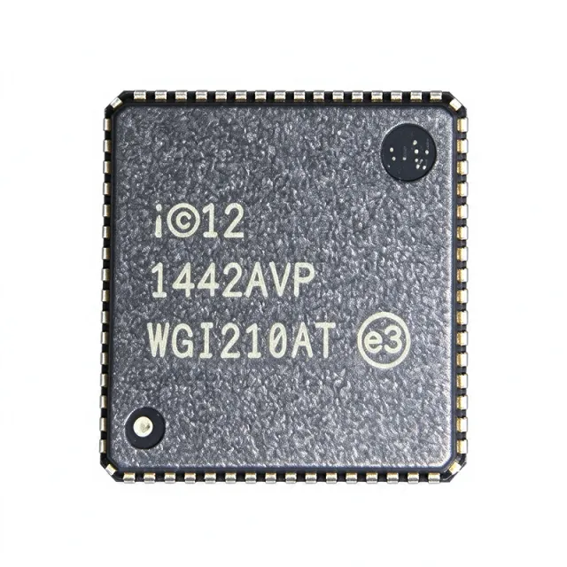
WGI210AT-SLJXR - Intel I210-AT GbE Ethernet Controller QFN-64
The Intel WGI210AT-SLJXR is an Intel Ethernet Controller I210-AT single-chip Gigabit Ethernet MAC + PHY in a 9x9 mm QFN-64 (9x9) package, supporting 10BASE-T, 100BASE-TX, and 1000BASE-T over PCIe, SGMII, SPI, JTAG, and I2C interfaces at 3.3 V supply and 0.9 V core. According to the I210-AT datasheet, the device integrates a GbE PHY with jumbo-frame support and Audio-Video Bridging / IEEE 802.1AS / 802.3az Energy Efficient Ethernet features for desktop, server, and embedded designs. An Ethernet controller is a mixed-signal integrated circuit that links a host system (typically a CPU or SoC) to a wired network, handling MAC address framing, PHY physical-layer termination, and offloading protocol tasks from the host CPU. It belongs to the broader network-interface category (NIC controller -> Ethernet controller -> mixed-signal IC -> semiconductor) and is essential wherever a deterministic, low-latency wired network connection is required. Ethernet controllers sit in the platform's input/output subsystem, bridging PCIe to copper media and providing the physical termination that magnetics and an RJ45 jack connect to. The I210-AT is Intel's mainstream GbE controller for non-server applications and supports the full media-negotiation trio of 10 Mbps, 100 Mbps, and 1000 Mbps. It exposes a PCIe v2.1 5 GT/s host interface for typical x1 edge-connector applications, alongside legacy SMBus, SPI, and JTAG for management and firmware update. Power is supplied through a 3.3 V main rail and a 0.9 V core rail, with full PHY-level Energy Efficient Ethernet (EEE) support reducing link power during idle periods. Industrial features include NC-SI / SMBus manageability, MAC address pre-programming, and platform firmware resiliency. Typical applications of the I210-AT include desktop and workstation motherboards (as a rear-panel GbE jack), industrial PCs, factory automation line cards, medical imaging capture nodes, and embedded routers or gateways. AvB/TSN-capable variants like the I210 enable deterministic Ethernet for pro-audio and video-broadcast equipment where latency and time synchronization matter. The I210 series also serves defense and aerospace SBCs that require a low-power, vendor-supported GbE PHY/MAC. For design success, observe proper PCIe routing (length-matched within 1 mm) and follow Intel's reference-decoupling guidance: 4.7 uF + 0.1 uF near each power pin with a solid ground return. Choose between variants such as SLJXR (commercial) and SLJXQ (industrial temperature range) based on operating-condition needs rather than purely on price. Designers using AVB/802.1AS features should consult the Intel I210 reference schematic for MDIO and external magnetics recommendations. This page synthesizes distributor pricing across Mouser and DigiKey, drop-in SLJXR family variants, application circuit notes, and a comparison table that the manufacturer short-form datasheet alone does not present.
WGI210IS - Intel I210-IS Gigabit Ethernet Controller QFN-64
The Intel WGI210IS is the industrial-temperature variant of the Intel® Ethernet Controller I210, a single-chip, low-power Gigabit Ethernet (10/100/1000 Mbps) controller with a PCI Express v2.1 (2.5 GT/s) host interface, packaged in a 64-pin QFN (9 mm × 9 mm) with exposed pad. Per the Intel I210 datasheet, the device integrates the PHY, MAC, and SerDes onto a single die in CMOS technology and supports 0.9 V / 3.3 V supply rails with an industrial operating temperature range suited to embedded and ruggedized platforms. Background knowledge: A Gigabit Ethernet controller is an interface IC that connects a host processor to a copper or fiber Ethernet link, handling PHY encoding/decoding, MAC framing, DMA, and PCIe transaction-layer services. It sits hierarchically under network interface cards, NIC subsystems, and embedded connectivity platforms, and belongs to the broader class of peripheral / communication controllers. Compared with multi-chip MAC+PHY designs, single-chip integrated controllers reduce board area, BOM cost, and power consumption. Key features include support for IEEE 802.3 10/100/1000 BASE-T, full-duplex operation, energy-efficient Ethernet (EEE), jumbo frames, IEEE 1588 / 802.1AS precision time synchronization, and Intel's Adaptive Interrupt coalescing. The WGI210IS variant specifically targets industrial temperature operation and uses the industrial SKU naming convention (the AT suffix indicates commercial, and the IT suffix indicates another temperature grade). Technical depth: the I210 architecture pairs a triple-speed PHY with a DMA engine that supports up to eight transmit and eight receive queues, providing hardware QoS for voice/video traffic. Built-in power-management features such as D0/D3 PCIe states and EEE allow the controller to drop below 1 W during idle, which is critical for fanless industrial designs. Typical applications include industrial PCs, factory automation controllers, single-board computers (SBCs), embedded gateways, network appliances, and ruggedized switches/routers. The PCIe v2.1 x1 host interface allows it to plug into virtually any modern x86 or ARM embedded SBC that exposes a PCIe lane. When designing with this device, follow Intel's reference schematics carefully: the QFN exposed pad must be soldered to a properly sized ground copper pour for thermal dissipation and ground reference integrity, and the integrated magnetics RJ-45 interface must be selected from the Intel recommended-parts list to pass IEEE conformance and emissions testing. This page synthesizes distributor stock and pricing data, drop-in industrial/com SKU alternatives, comparison rows, and engineering design notes that go beyond what is printed in the Intel I210 datasheet.