Gestion de l'alimentation
Sous-catégories
Produits (2819)

STSPIN220 - 1/256 Microstep Stepper Driver QFN-16 | STMicroelectronics
The STMicroelectronics STSPIN220 is a low-voltage bipolar stepper motor driver integrating a microstepping sequencer with up to 1/256-step resolution, two PWM current controllers, and a power stage composed of two fully protected full-bridges, housed in a compact 16-pin VFQFPN (3x3x1.0 mm) package. A stepper motor driver is a power management IC that translates low-power control signals into the sequenced phase currents required by bipolar stepper motors. Within the semiconductor hierarchy it sits under motor drivers and motor control ICs, bridging the gap between a microcontroller and the motor coil load. Stepper drivers combine logic (sequencer, translator), current regulation (PWM choppers), and a power stage (H-bridges) in a single device, replacing discrete transistor bridges and simplifying motion-control design. Key features of the STSPIN220 include microstepping resolution as fine as 1/256 of a step for smooth, low-audible-noise motion, an integrated PWM current controller with fixed off-time for accurate coil current regulation, and a low RDS(on) power MOSFET output stage that minimizes conduction losses and heat generation. The device also integrates a full set of protection features, and supports a simple Step/Direction control interface compatible with common 3D-printer and motion-control host architectures. From a technical standpoint, the two fully protected full-bridges drive both phases of a bipolar stepper, while the internal sequencer generates the microstep current profile selected through the microstep mode pins. The PWM current controllers compare the voltage across an external sense element with the reference set by VREF, regulating phase current with fixed off-time chopping. Fully protected operation covers overcurrent and thermal fault conditions, improving system robustness in cost-sensitive designs. Typical applications include 3D printers and 3D-printer stepper driver boards, small robotics and camera-gimbal positioning, laboratory automation, portable battery-powered devices, and low-voltage bipolar stepper actuation up to the 10 V motor-supply class. Its 3x3 mm VFQFPN footprint makes it attractive for space-constrained carrier boards. For design, size the sense resistor so full-scale coil current matches the VREF setting, and provide adequate copper area on the exposed pad for thermal dissipation at higher currents. This page synthesizes distributor pricing, lifecycle information, and application guidance not found in the manufacturer datasheet alone.

STSPIN32F0601TR - 600V 3-Phase BLDC SiP | STM32 | STMicroelectronics
The STMicroelectronics STSPIN32F0601TR is an advanced 600 V three-phase BLDC (brushless DC) motor controller system-in-package (SiP) integrating an ARM Cortex-M0 STM32 microcontroller with 32 KB Flash, a smart gate driver capable of driving N-channel power MOSFETs or IGBTs up to 600 V, and a wide-input linear regulator on a single 64-pin TQFP exposed-pad substrate. Operating from 9 V to 20 V on the supply rail with an embedded 12 V LDO for the gate driver, the device targets home appliances and industrial drives where PCB area, BOM count and reliability dominate the design trade-off. Key headline specs include a 48 MHz Cortex-M0 CPU, 32 KB embedded Flash, 600 V high-voltage rail tolerance on the gate-driver outputs, integrated bootstrap diodes for the three high-side drivers, less than 1 V gate low-level output at 10 mA sink (eliminating external bleeder resistors), an active-low shutdown EN pin, and a smart shutdown comparator that protects the power stage from over-current events. The TQFP-64 10x10 mm package with exposed thermal pad keeps dissipated heat inside the inverter footprint. An LDO (Low-Dropout) linear regulator inside this SiP steps the purpose of a voltage regulator that maintains a stable output even when the input-to-output differential is small; here the 12 V LDO derives the gate-driver VCC from the motor bus, while the MCU core is fed from a separate low-voltage regulator on the same die. The system-in-package concept itself sits within the broader motor-control hierarchy: motor driver IC -> gate driver -> motor controller -> power management IC -> semiconductor. This layered integration is the primary engineering reason designers choose STSPIN32F0601 over a discrete MCU + gate-driver solution. Typical applications include 600 V-class three-phase BLDC/PMSM drives for washing machines, refrigerators, air-conditioner compressors, fans, pumps, industrial servo pumps, and e-bike industrial controllers. The integration also benefits HVAC blower systems and small industrial drives where every millimetre of PCB real estate is at a premium. When laying out the PCB, place the bootstrap capacitors as close as possible to the high-side pins and use a 4-layer board with a continuous ground plane under the exposed pad for thermal relief. Verify that the shunt-resistor value is sized so that the smart-shutdown comparator threshold (200 mV typical on the SD pin) trips before the external MOSFETs exceed their SOA. The SiP is not a hot-swap part; allow at least 1 ms for VCC ramp-up before asserting EN high. This page synthesizes distributor pricing, drop-in same-package alternatives, and practical SiP layout notes that are not found in the manufacturer datasheet, supporting engineers in selecting and qualifying the STSPIN32F0601TR for next-generation high-voltage motor drives.
STSPIN32F0602 - 600V Three-Phase BLDC SiP | STMicroelectronics
The STMicroelectronics STSPIN32F0602 is an advanced 600 V three-phase brushless DC (BLDC) controller system-in-package (SiP) that integrates a high-voltage gate driver with an ARM Cortex-M0 STM32 microcontroller in a single 64-pin TQFP exposed-pad package. The high-voltage rail tolerates up to 600 V and the device pairs with external power switches to build complete three-phase inverters for industrial drives, white goods, and home appliances. A system-in-package for motor control combines an MCU core, gate drivers, and housekeeping supplies in a single molded body, dramatically shrinking PCB footprint and bill-of-material versus a discrete implementation. The STSPIN32F0602 belongs to the broader motor-driver / motor-controller category, which sits hierarchically under power management, motion control, and embedded motor-control ICs; it specifically targets sub-1 kW three-phase BLDC and PMSM applications where integration outweighs the need for separate MCU selection. Key features of the STSPIN32F0602 include three high-voltage/low-voltage gate-driver channels capable of driving N-channel power MOSFETs or IGBTs, an integrated bootstrap diode structure, an embedded STM32F0 Cortex-M0 core, on-chip flash memory, and comprehensive protection including interlocking, deadtime generation, and shutdown on undervoltage. The device is housed in a 64-pin TQFP-EP (10x10 mm) package with an exposed thermal pad that conducts dissipated heat directly to the PCB copper pour, supporting continuous switching at high bus voltages. Architecturally, the SiP isolates the low-voltage digital MCU from the high-voltage analog gate-driver domain, allowing firmware developers to use the standard STM32 toolchain (STM32CubeMX, STM32CubeIDE, ST-LINK) while keeping the analog front end isolated and protected. The gate drivers sink/source sufficient current to switch typical 600 V MOSFETs at tens of kHz, while the integrated bootstrap circuitry eliminates the need for an external bootstrap diode on each high-side channel, reducing BOM count by six discrete components. Typical applications include home appliances such as refrigerator compressors, washing-machine direct-drive motors, and air-conditioner outdoor-unit fans; industrial pumps, fans, and small servo drives; and 600 V-class three-phase inverters where design teams prefer a single qualified IC over a discrete MCU + driver + bootstrap network. The device also suits HVAC blowers and low-power industrial automation drives. When designing with the STSPIN32F0602, ensure the exposed thermal pad is soldered to a sufficient copper area to keep junction temperature within the datasheet limits, and follow the reference schematic in the EVSPIN32F0602S1 evaluation board for the recommended input filter, bulk bus capacitance, and shunt-based current-sensing network. Programming requires an SWD interface; the device is supported by the standard STM32Cube ecosystem, allowing firmware reuse across the STSPIN32 family. This page synthesizes distributor pricing, parametric drop-in alternatives, and practical design notes not found in the manufacturer datasheet alone. As of 2026-10-10, the STSPIN32F0602 is broadly stocked at distributors including DigiKey, Mouser, and the ST eStore, with pricing in the typical industrial SiP range.

STUSB1702YQTR - USB Type-C PD Controller with TX/RX Line Driver | STMicroelectronics
The STMicroelectronics STUSB1702YQTR is a USB Type-C port controller with integrated TX/RX line driver and BMC (Biphase Mark Coding) transceiver, qualified to AEC-Q100 and supplied in a 24-pin QFN EP (4x4 mm wettable flanks) package. It implements a USB Type-C source controller with VBUS power switch, dead-battery support, and USB Power Delivery (PD) message handling for USB 2.0 and SuperSpeed USB 3.0 signaling paths. The device operates over a supply range of 4.1 V to 22 V with a -40 C to +105 C operating temperature window, and the wettable-flank QFN-24 (QFN24 EP 4x4 mm) package enables automated optical inspection for automotive applications. Key features include USB Type-C cable attach and orientation detection (CC1/CC2 logic), USB PD 2.0 / 3.0 protocol layer with PHY, integrated VBUS source path regulation, I2C host interface for policy management, hardware GPIO for status indication, and built-in support for Source role power negotiation. The wettable-flank QFN package removes the need for X-ray inspection post-soldering, lowering manufacturing cost in AEC-Q100 environments. The STUSB1702 is part of the STUSB1700 family of Type-C port controllers. Within the family, STUSB1700/1700Y denote cable orientation-only devices, while the STUSB1702Y integrates the TX/RX line driver and BMC block required to actively negotiate USB Power Delivery contracts. Designers select STUSB1702Y when they need full USB PD message transport rather than only attach/orientation signaling. Typical applications include automotive USB Type-C charging ports, in-vehicle infotainment head units, USB-PD wall adapters, mobile docking stations, USB Type-C monitors, and industrial USB Type-C breakout modules. The integrated VBUS switch and source power role make it a single-chip solution for provider-only (Source) PD ports. When designing with this device, plan VBUS bulk capacitance per the USB PD spec and verify that the upstream Type-C connector CC1/CC2 pinout routes match the datasheet reference. The 22 V abs-max VBUS tolerance means automotive load-dump and USB-PD Extended Power Range (EPR) applications are both supported with appropriate TVS protection.
STUSB4531QTR - USB PD Sink Controller I2C QFN-16 | ST
The STMicroelectronics STUSB4531QTR is a standalone USB Type-C Power Delivery (PD) sink controller with an I2C interface, housed in a 16-pin QFN (3x3 mm) package. It negotiates up to five configurable Power Data Objects (PDOs) supporting 5V, 9V, 12V, 15V and 18V sink profiles, and operates without any external microcontroller firmware thanks to a PDO configuration stored in internal non-volatile memory. A USB PD sink controller is a power management interface IC that implements the USB Type-C connector attach/detect state machine and the USB PD protocol on the CC (Configuration Channel) pins, allowing a powered device to request higher voltages and currents from a PD source. It sits in the system hierarchy between the physical USB-C receptacle and the downstream DC-DC converter or battery charger, translating the negotiated contract into VBUS connect/disconnect control and voltage selection signals. Key features of the STUSB4531 include fully autonomous negotiation (autorun mode) that requires no software support, making it ideal for automatic high-power profile charging; a hybrid mode that allows an embedded host to override or monitor negotiation via the I2C interface; and always-on dead battery mode, which presents CC pull-down terminations even when the device is unpowered, so a fully depleted battery (SOC = 0%) can still be charged directly from the VBUS receptacle pins. Technically, the STUSB4531 integrates the CC line termination logic, BMC transceivers, PD protocol engine, and NVM-based configuration in a single die. VBUS_EN_SNK provides the sink VBUS power-path enable output, and the GATE pin supports external NMOS VBUS switch control. The I2C interface exposes status registers, alert interrupts, and allows runtime PDO modification without reprogramming the NVM. Typical applications include USB-C powered monitors, docks and hubs, battery-powered consumer devices requiring dead-battery charging, industrial equipment with USB-C power inputs, and any sink-only system that needs PD negotiation without a firmware investment. Designers should note that dead battery mode is always active on the QTR and BJR variants, ensuring source attach even with zero system power. A key design consideration is that the device is powered directly from VBUS through the VDD pin, so layout should keep the VBUS sense and CC traces short and matched, and the VBUS_EN_SNK pin can be left unconnected if the power path is controlled elsewhere while negotiation still proceeds over CC. This page synthesizes distributor pricing, drop-in alternatives, and practical design notes not found in the manufacturer datasheet.

Si8271GB-ISR - 4A Isolated Gate Driver, 2.5kV, 8-SOIC | Skyworks
The Skyworks Solutions Si8271GB-ISR is a 4 A galvanically-isolated single-channel gate driver with 2.5 kV RMS withstand voltage, housed in a narrow-body 8-pin SOIC (SO-8) package. It delivers 4 A peak source/sink drive current with a typical propagation delay of 50 ns and high CMTI of 400 kV/µs for switching power MOSFETs, IGBTs, and SiC/GaN HEMTs. An isolated gate driver is a galvanic isolation barrier combined with a high-current buffer stage, used to drive the gate of a high-side or low-side power transistor while protecting low-voltage control logic from high-voltage transients. The isolated gate driver category sits within the power management hierarchy: gate driver -> driver IC -> power management IC -> semiconductor. Si827x-family parts use proprietary silicon-oxide isolation instead of optocouplers or transformers, which eliminates LED-aging concerns and provides tight timing characteristics. Key features include 4 A peak output current, 30 ns typical propagation delay, 400 kV/µs common-mode transient immunity (CMTI), 2.5 kV RMS isolation per UL1577, integrated UVLO with 3 V threshold for IGBT/SiC protection, de-glitch input filtering, and a programmable dead-time (DT) pin. The narrow-body 8-SOIC footprint is pin-compatible with common opto-isolated gate drivers, enabling direct PCB replacement in many designs. The device uses Skyworks' proprietary silicon isolation technology based on RF-coupled differential transmission across a high-voltage silicon-oxide barrier. This approach eliminates the lifetime and CTR degradation inherent in optocouplers, and avoids the high-frequency emissions and large footprint of pulse transformers. The driver outputs swing rail-to-rail from VDD to GND on each side, supporting both +12 V and unipolar gate-drive rails. Typical applications include driving IGBTs in motor-control inverters, SiC MOSFETs in EV traction and onboard chargers, GaN HEMTs in telecom DC-DC bricks, solar inverters, industrial SMPS half-bridge stages, and digital-isolation upgrades for opto-coupler-based legacy designs. The wide driver supply range supports both 5 V and 12/15 V gate-drive rails. When designing with this part, place a 100 nF decoupling capacitor close to each VDD pin and a 4.7 µF bulk capacitor on the output-side VDD. For half-bridge use, the programmable dead-time pin prevents shoot-through; consult the manufacturer datasheet for the DT resistor selection table.

TAS5760L 21W Stereo I2S Class-D Audio Amplifier | TI
The Texas Instruments TAS5760L (TAS5760LDDCA) is a flexible, general-purpose stereo Class-D speaker amplifier with a digital I2S input serial audio port, delivering 21 W per channel in stereo or 42 W mono into a BTL load from a single 4.5 V to 16.4 V supply in a 48-pin HTSSOP package with exposed thermal pad. A Class-D audio amplifier is a switching amplifier that uses PWM modulation of power output stages to achieve efficiencies far above linear Class-AB designs, typically above 85-90 percent. Within the power-management and audio-signal-chain hierarchy, the TAS5760L sits between a digital audio source (SoC, DSP, or MCU with I2S/TDM output) and the loudspeaker, integrating DAC, processing, and power stage in one IC, reducing board area and EMI-filtering complexity compared to discrete solutions. Key features include both hardware-mode (strap-pin) and software-mode (I2C) control, an integrated digital clipper that protects speakers from overdriven signals, multiple gain settings, and two speed modes supporting a wide range of audio clock configurations. The 48-pin package also integrates a headphone or line-output driver path, eliminating an external DAC-headphone amplifier in many designs. Architecturally, the TAS5760L processes the incoming I2S stream digitally - including volume, EQ-based gain options, and clipping control - before driving a closed- or open-loop PWM power stage with integrated FETs. This digital-in architecture avoids the noise and mismatch of an external analog DAC-to-amp path and keeps the audio signal in the digital domain until final amplification. Typical applications include smart speakers and voice-assistant devices, portable Bluetooth speakers, soundbars, TV audio, and general-purpose powered-speaker designs. The wide 4.5 V to 16.4 V supply range covers single lithium-ion battery packs through 12 V wall adapters. Design tip: choose hardware mode for lowest BOM cost, but software mode (I2C) unlocks the full register set for volume, EQ, and diagnostics; always provide adequate copper area under the thermal pad for the 42 W mono condition.
TB6600 - 5A Stepper Motor Driver IC | Toshiba | CNC
The Toshiba TB6600 (TB6600HG) is a 1-channel bipolar stepping motor driver IC rated for 50V motor supply and 5A (4.0A peak in typical module implementations) output current, delivering microstepping resolution up to 1/16 step in a 25-pin HZIP (HZIP25) power package with integrated MOSFET output bridges. A stepping motor driver IC is a power management device that converts low-current logic-level STEP and DIR pulse signals from a microcontroller into high-current phase currents required by a stepper motor. Within the power electronics hierarchy, it sits between the motor controller (MCU or CNC breakout board) and the motor windings, performing current regulation, microstepping interpolation, and protection functions in a single package. Key features include a wide 9V to 40V DC motor supply range on typical module implementations, output current selectable in 8 steps from 0.7A to 4.0A via DIP switches, and a maximum input pulse frequency of 20 kHz. The device integrates under-voltage lockout (UVLO), over-current detection (ISD), and thermal shutdown (TSD) protection circuits, per the Toshiba product page. The TB6600 uses bipolar power MOSFET output stages in an H-bridge arrangement for each phase, enabling full bipolar drive of 2-phase and 4-phase hybrid stepper motors. Microstepping up to 1/16 reduces torque ripple and audible noise compared with full-step drive. The decoded current decay control maintains smooth phase-current waveforms across the speed range. Typical applications include DIY and light-duty CNC routers, 3D printers driving NEMA 17 and NEMA 23 motors, engraving machines, and small robotics, where optocoupler-isolated signal inputs (on common TB6600 modules) protect the controller from motor-side voltage transients. Design consideration: thermal management dominates the design - at 4A the HZIP package requires a substantial aluminum heatsink, and the manufacturer notes the part is not intended for professional-grade applications. This page synthesizes distributor data, verified specifications, comparisons against DM542, A4988, and TMC2209, and practical design notes not found in the manufacturer datasheet.

TB67H420FTG - 50V 9A Dual H-Bridge Brushed DC Motor Driver | Toshiba
The Toshiba TB67H420FTG is a brushed DC motor driver IC supporting high-current (9.0 A) and high-voltage (50 V) operation, housed in a 48-pin VQFN (7 mm x 7 mm) package. Built on Toshiba's BiCD process, it integrates dual H-bridges that can be controlled independently for two brushed DC motors or in parallel for a single higher-current stepping/brush load, and uses sense-resistor-less PWM current control for simplified board layout. A brushed DC motor driver is a power-integrated circuit that converts low-current logic-level PWM signals from a microcontroller into high-current drive outputs capable of energizing the motor windings. By eliminating external current-sense resistors, sense-resistor-less architectures reduce BOM cost, shrink PCB area, and simplify wiring in cost-sensitive H-bridge designs. The TB67H420FTG sits in the broader taxonomy: H-bridge driver -> motor driver IC -> power management IC -> semiconductor, making it a foundational block for mechatronic subsystems. Key specifications include an absolute maximum supply voltage of 50 V, a peak output current of 9.0 A (continuous ~4.5 A per the official Toshiba product page), built-in Under-Voltage Lockout (UVLO), Thermal Shutdown (TSD), and Intelligent Shutdown (ISD) protection. The device operates from a single power supply (VM) with logic-level inputs, and supports forward, reverse, brake, and Hi-Z modes through standard IN1/IN2 control logic. Fabricated on BiCD (Bipolar + CMOS + DMOS) process technology, the TB67H420FTG combines low-loss DMOS output stages with CMOS control logic on a single die, enabling high-efficiency switching and small package footprint. The exposed thermal pad on the VQFN-48 package provides a low-thermal-resistance path (theta-JA per datasheet) essential for continuous high-current operation. Typical applications include dual brushed DC motor control in robotics and small CNC machines, single-axis stepper motor driving in 3D printers, automated curtain/blind drives, and battery-powered e-mobility toys where 24-36 V battery packs are common. The dual H-bridge mode is also suitable for bipolar stepper control up to the rated current. The 50 V absolute maximum provides substantial margin above 24 V and 36 V industrial bus rails. When designing with this device, always include adequate bulk decoupling on VM (typically 100 uF electrolytic + 10 uF ceramic) placed adjacent to the IC. The exposed thermal pad MUST be soldered to a sufficiently large copper pour (recommended >= 1 square inch) to achieve the rated continuous current without triggering thermal shutdown. Confirm operating mode (dual brushed vs single stepping) before PCB layout, since pin mapping differs. This page consolidates distributor pricing, drop-in compatible same-brand alternates, and practical design notes that complement the manufacturer datasheet - information not found in a single source on the manufacturer site.

TBD62503AFNG - 7-Ch DMOS Sink Driver Array 50V/0.3A | Toshiba
The Toshiba TBD62503AFNG is a 7-channel sink-type DMOS transistor array housed in a 16-pin SSOP package, capable of switching loads up to 50V and 300 mA per channel. Built on Toshiba's BiCD (Bipolar, CMOS, DMOS) monolithic silicon process, the device integrates seven open-drain N-channel DMOS output transistors that share a common ground return, making it ideal for low-side switching of relays, solenoids, lamps, LED displays, and logic-level buffers. A DMOS transistor array is a type of power driver IC that uses seven discrete N-channel double-diffused MOS transistors integrated onto a single silicon die, each with its own gate and drain pin and a shared source (substrate) tied to ground. This monolithic array category sits within the broader power management and driver IC taxonomy: transistor array -> peripheral driver -> interface IC -> semiconductor. The 50V drain-to-source breakdown and 0.3A continuous drain current make it well-suited for industrial control boards and 24V industrial bus switching. Key features include a wide operating supply range of up to 50V on the drain side, low on-resistance DMOS outputs that minimize conduction losses versus bipolar Darlingtons, 3V CMOS/TTL-compatible logic inputs, and built-in clamping diodes for inductive loads. Each of the seven channels can be driven independently from a microcontroller GPIO or logic gate, with output currents of 300 mA continuous and pulse handling exceeding 500 mA per channel. The architecture is optimized for digital-logic-to-load interfacing: each input pin drives a MOSFET gate through a CMOS inverter stage, while the output stage is a DMOS open-drain switch with intrinsic body diode protection. Because the outputs are N-channel low-side switches rather than Darlington pairs, the on-resistance stays in the low-ohm range across the full temperature range, eliminating the classic bipolar Vce(sat) loss that wastes power as heat in legacy ULN2003-style arrays. Typical applications include programmable logic controller (PLC) digital output modules, LED matrix and seven-segment display drivers, relay and solenoid driver boards, and unipolar stepper motor driving where multiple low-side channels are required. The SSOP-16 footprint is also compatible with breadboard-friendly adapter boards for prototyping. When designing with this part, note that it is a sink (low-side) driver only - loads must be tied to the positive supply. Each output requires flyback protection for inductive loads; the device integrates a body diode, but external Schottky or fast-recovery diodes are recommended above 100 mA inductive currents to keep thermal dissipation under control. This page synthesizes distributor pricing, drop-in alternatives, and practical design notes not found in the manufacturer datasheet alone.
TC1232EOA - Processor Supervisor w/ Watchdog | Microchip
The Microchip Technology TC1232EOA is a fully-integrated microprocessor monitor that combines precision power-on reset control, a watchdog timer, and external reset override in a single 8-pin SOIC package. According to the manufacturer datasheet, the device monitors a single supply rail with a factory-trimmed threshold range of 4.5 V to 4.75 V and asserts an active-low reset output for a minimum of 250 ms after VCC stabilizes above the threshold. The reset output is open-drain or open-collector, allowing wired-OR connection with other system reset sources. What is a microprocessor supervisor? A microprocessor supervisor (also called a voltage supervisor or reset IC) is a dedicated power management IC that protects a microprocessor or microcontroller from undervoltage, brownout, and code-execution faults. It sits in the power management hierarchy between the DC-DC converter or LDO (which provides the rail) and the MCU itself, forming the third tier of protection after voltage regulation and input protection. Supervisors are essential where deterministic boot behavior and watchdog enforcement are required, distinguishing them from simple comparators or POL converters. Key features of the TC1232EOA include an adjustable watchdog timebase of 150 ms, 600 ms, or 1200 ms selectable via the TD pin, no requirement for external timing components, and a low quiescent supply current that minimizes battery drain. The PBRST input allows an external push-button or system controller to force a manual reset without an additional debounce circuit. The wide operating supply range of 1.2 V to 5.5 V makes it compatible with both 3.3 V and 5 V microprocessor families. Technically, the TC1232EOA uses a precision bandgap reference combined with a comparator to detect undervoltage conditions with tight threshold accuracy across the full industrial temperature range. The internal watchdog state machine expects a negative-going edge on the ST input within the selected timeout window; if no edge arrives, /RESET is asserted. The watchdog is fully disabled by tying TD to VCC, simplifying BOM on boards that do not require watchdog supervision. Typical applications include embedded MCU reset control, industrial PLC and sensor node brownout protection, automotive body controller watchdog supervision, point-of-sale terminal power supervision, and any battery-powered system that requires deterministic start-up after cold-boot or brownout recovery. Design consideration: choose the watchdog timeout based on the longest legitimate loop iteration in your firmware; setting it too short triggers spurious resets while setting it too long delays fault detection. Place the supervisor close to the MCU reset pin and use a 10 kohm pull-up on the open-drain reset line. This page synthesizes distributor pricing, drop-in alternatives, and practical design notes not found in the manufacturer datasheet.
TC7660SCOA - 20mA Super Charge Pump Inverter | Microchip 8-SOIC
The Microchip TC7660SCOA is a 20 mA super charge pump DC-to-DC voltage converter in an 8-pin SOIC package that inverts +1.5V to +12V input to a corresponding -1.5V to -12V output using only two low-cost capacitors. The 'S' variant upgrades the industry-standard TC7660 with extended supply range, higher efficiency (98% typ), and lower quiescent current of 80 µA typ at VIN = 5V, eliminating inductors and the associated cost, board area, and EMI. A charge pump (also called a switched-capacitor voltage inverter) is a type of DC-DC converter that uses capacitors rather than inductors to store and transfer energy. Charge pumps belong to the switched-capacitor converter family within the broader power management IC hierarchy. Unlike inductive buck/boost converters, charge pumps are EMI-quiet and use only two external capacitors, making them ideal for low-current negative rail generation where simplicity and noise performance outweigh efficiency. Key features include 99.9% voltage conversion efficiency (typ), 20 mA output current capability, wide input voltage range up to +12V (vs 10V for original TC7660), and on-board oscillator at nominal 10 kHz frequency. The TC7660SCOA also supports a BOOST pin for higher switching frequencies when needed. The 8-SOIC package operates over -40°C to +85°C industrial temperature range with surface-mount assembly. The architecture uses a CMOS switched-capacitor voltage inverter with integrated MOSFET switches clocked by an internal RC oscillator. The doubler/inverter topology transfers charge from input to reservoir capacitor on one clock phase and inverts on the other, producing a negative output without inductors or transformers. The result is a compact, low-noise negative supply solution with predictable EMI signature. Typical applications include op-amp negative supply rails, LCD bias generators, data acquisition systems, EIA-232/EIA-422 level translators, and portable instrument negative rails. The 20 mA output comfortably drives a single op-amp negative rail or a small RS-232 transceiver charge pump supplement. When designing with this device, ensure external reservoir and pump capacitors are low-ESR types rated for the switching frequency, and observe the LV pin voltage derating requirements above +10V input to maintain reliability. This page synthesizes distributor pricing, drop-in alternatives, and practical design notes not found in the manufacturer datasheet.
TC7660SEOA - 20mA Super Charge Pump DC-DC Converter | Microchip
The Microchip Technology TC7660SEOA is a super charge pump DC-to-DC voltage converter that delivers up to 20 mA of negative output current from a +1.5 V to +12 V input, housed in an 8-pin SOIC (0.154", 3.90 mm width) package. It functions as an inverted switched-capacitor regulator that produces -Vin or 2Vin selectable output with only two external capacitors, eliminating inductors and their associated cost, size, and EMI. A charge pump DC-DC converter is a type of switching voltage regulator that uses capacitors rather than magnetic inductors to store and transfer energy. Charge pumps sit within the broader hierarchy of DC-DC converters -> switching regulators -> power management ICs -> semiconductors. They are favored in low-power, noise-sensitive designs because they generate no magnetic EMI and require only two capacitors, making them ideal for compact analog front ends where a small negative supply rail is needed without the bulk of an inverting buck-boost converter. Key features of the TC7660SEOA include pin-compatibility with the industry-standard 7660 footprint, a wide 1.5 V to 12 V input range that can be doubled to 12 V to 24 V using the internal oscillator doubling mode, and a typical quiescent current in the microamp range. The on-board CMOS oscillator nominally operates at 10 kHz, with an optional external clock input for synchronization. The device includes a BOOST pin reference, low output impedance (~55 ohm typical), and operates across the -40C to +85C commercial temperature range, suiting RS-232 drivers, op-amp negative rails, and portable instrumentation. Internally, the TC7660SEOA uses CMOS transistors configured as an H-bridge switched-capacitor network clocked by the on-chip oscillator. During one clock phase, the flying capacitor is charged to +Vin; during the alternate phase, it is flipped and discharged into the reservoir capacitor at -Vin. The architecture avoids the switching spikes common to inductive converters, and its symmetrical pinout supports cascading two devices for voltage doubling. Typical applications include generating the -5 V to -12 V rail for RS-232 transceivers, negative bias supplies for op-amps and LCD contrast, low-current analog signal conditioning, and portable data-acquisition systems. When designing with this device, keep the flying capacitor ESR low (typically 10 uF) and place reservoir capacitors close to pins 5 and 8 to minimize ripple and load-transient overshoot. This page synthesizes distributor pricing, drop-in alternatives, and practical design notes that go beyond the manufacturer datasheet to help engineers select and source the TC7660SEOA with confidence.

TC78H660FNGEL - 18V/2A Dual H-Bridge Motor Driver | Toshiba
The Toshiba TC78H660FNGEL is a dual-channel brushed DC motor driver IC that integrates two DMOS H-bridges in a 16-pin TSSOP package, rated for 2.0 A peak output current per channel and an operating supply range of 2.5 V to 18 V. According to the Toshiba product page, this IC can drive two DC brushed motors independently or one bipolar stepping motor, and includes built-in low-voltage lockout (UVLO), thermal shutdown (TSD), and overcurrent shutdown (ISD) protection. The on-chip DMOS output transistors deliver low on-resistance (typically around 0.5 ohm per HS+LS FET at room temperature) which reduces conduction loss and improves thermal headroom in compact 16-TSSOP layouts. A brushed DC motor driver is a power-management IC that uses full-bridge or half-bridge switching stages to commutate a permanent-magnet DC motor electronically, replacing mechanical brushes with MOSFETs. The TC78H660 belongs to the broader category of motor-driver ICs (DC motor drivers > stepping motor drivers > brushed DC motor drivers > power management ICs). Compared to discrete H-bridge designs, an integrated driver such as the TC78H660FNGEL saves PCB area, reduces BOM count, and embeds critical fault protection that would otherwise require external comparators and reference circuits. Key features include 2.0 A peak / 1.4 A continuous per channel, 2.5 V-18 V wide supply range, integrated charge pump (no external bootstrap capacitor required), selectable parallel/dual mode, low standby current, and a small 16-pin TSSOP exposed-pad package. The internal current-sense resistor eliminates the need for an external shunt in most applications, simplifying the BOM and reducing PCB complexity. Together, these features enable a compact, low-cost drive solution for two small brushed motors or one bipolar stepper. Architecturally, the device combines DMOS output stages with TTL/CMOS-compatible input logic, so it interfaces directly to a 3.3 V MCU without level shifters. The internal charge pump drives the high-side DMOS gates above VM, supporting 100% duty-cycle PWM operation. Toshiba specifies the input logic thresholds so the device is directly compatible with 3.3 V GPIO. Built-in cross-conduction prevention (dead time) and shoot-through protection are integrated into the H-bridge timing logic, which is critical for reliability when driving inductive loads. Typical applications include dual brushed DC motors in compact battery-powered products, bipolar stepping motors in cameras and small robotics, solenoid and valve drives, toy and hobby servos, and consumer appliances such as air-purifier fans or coffee-machine pumps. Because the device runs from a single 2.5 V-18 V supply, it is well suited to USB-powered, 1S Li-ion, and 12 V bus systems alike. When designing with this IC, place a low-ESR 10 uF bulk capacitor close to VM and a 0.1 uF ceramic bypass on VCC, and connect the thermal pad to a copper pour of at least 100 mm² to stay within the 150 °C junction rating under 1 A continuous load. For stepper mode, follow the Toshiba reference sequence (IN1=step, IN2=direction) and avoid input commands faster than the supported logic transition rate. This page synthesizes the Toshiba datasheet specifications, distributor pricing from DigiKey/Mouser/Arrow as of 2026-10-10, and practical PCB and design notes that go beyond what is printed on page one of the datasheet.

TC78H660FTG - Dual H-Bridge DMOS Motor Driver, 18V, 2A | Toshiba
The Toshiba TC78H660FTG is a dual-channel brushed DC motor driver IC that integrates two DMOS H-Bridges with low on-resistance output transistors in a 16-pin VQFN (3x3 mm) package. It operates from a 1.8V to 18V supply range and delivers up to 2A peak output current per channel, making it suitable for driving two DC brushed motors or one bipolar stepping motor from a single IC. A brushed DC motor driver is a power-management IC that converts low-power logic-level control signals into the high-current push-pull drive required by a brushed DC motor. Within the broader taxonomy, brushed DC motor drivers sit under motor driver ICs, then power management ICs, then semiconductor devices. The dual H-Bridge topology places four DMOS switches per channel so current can be steered in both directions through the motor winding, enabling forward, reverse, and braking functions from a small surface-mount part. Key features include 0.6 ohm (typical) on-resistance per DMOS output, integrated Undervoltage Lockout (UVLO), Overcurrent Detection (ISD), and Thermal Shutdown (TSD). A combined MODE/ERR pin lets a host MCU set operating mode in normal operation while the same pin asserts a low-level fault flag when TSD or ISD is triggered. Pulse-width modulation up to 200 kHz is supported for speed control, and logic inputs are 1.8V-compatible for direct connection to modern low-voltage MCUs. The TC78H660FTG uses Toshiba's proprietary CD-process DMOS transistors, which combine the low conduction loss of DMOS with logic-level gate drive, eliminating the need for external gate-drive circuitry. The exposed thermal pad on the VQFN-16 package lowers thermal resistance to roughly 35 C/W on a 4-layer 1 oz PCB, allowing 2A continuous operation at modest VIN without an external heatsink. Typical applications include 5V/12V dual brushed DC motors in robotics and small appliances, camera pan/tilt heads, vending-machine actuators, USB-powered fans and pumps, and bipolar stepper motors in compact mechanisms. The 18V absolute maximum supply simplifies 2-cell Li-ion (8.4V) and 12V industrial bus designs. When designing with this part, place input and motor bypass capacitors within 3 mm of their respective pins, and stitch the exposed thermal pad to a copper ground plane to keep junction temperature within safe limits at full 2A load. This page synthesizes distributor pricing, verified drop-in alternatives, and PCB-level design notes that go beyond the manufacturer datasheet to help engineers shorten the selection and qualification cycle.

TCA6507PW - 7-Bit I2C/SMBus LED Driver, 14-TSSOP | Texas Instruments
The Texas Instruments TCA6507PW is a 7-bit low-voltage LED driver with I2C and SMBus interface, supporting output current up to 40 mA per channel across 7 outputs in a 14-pin TSSOP (PW) package. It operates from a 1.65 V to 5.5 V supply range and is designed to control or dim LEDs through the two-wire bidirectional bus without continuous microcontroller involvement, freeing valuable processor time for other tasks. Background: A LED driver IC is a power-management semiconductor that regulates current through light-emitting diodes and provides brightness control. The TCA6507PW belongs to the I2C/SMBus-controlled LED driver category, which sits within the broader LED driver family inside power-management ICs. These devices relieve the host microcontroller from PWM-timing chores by generating the dimming waveform autonomously, while remaining configurable through a standard two-wire serial interface. Typical use cases are status indicators, keypad backlights, RGB funlights, and small LCD bias/supply chains. The 7-bit architecture means each of the seven outputs can be programmed independently, supporting combination of on/off and PWM brightness states simultaneously. Key features: seven programmable outputs selectable as on, off, slow on/off (programmable blink rates), or PWM dimming; software shutdown mode with a dedicated configuration register; per-pin 40 mA sink capability; 1.65 V to 5.5 V VCC range; integrated I2C/SMBus slave with selectable address; 25 mA quiescent current; and small-footprint 14-TSSOP (PW) package with 4.40 mm body width. The integrated brightness-control logic supports two user-selectable blink rates per output, allowing designers to mix steady-on indicators with blinking alerts without MCU overhead. Architecture: internally the TCA6507PW combines an I2C/SMBus-compatible serial interface, a bank of seven configurable output drivers with open-drain architecture, and a control register that selects between four modes per pin. The device operates as a slave on the I2C bus, with three address pins allowing up to eight TCA6507 devices on a single bus for expandability. The open-drain outputs can both sink current to drive LEDs tied to VCC, and accept logic-level inputs read back through the input register. Typical applications: LED status indication on routers/switches, mobile-phone keypad and funlight control, ultra-mobile PC indicator panels, industrial HMI status lamps, and any I2C/SMBus-backed multi-LED front panel. The TSSOP package suits compact handheld and space-constrained mainboards. Design consideration: place a 0.1 uF decoupling capacitor close to VCC (pin 14) and route the I2C SCL/SDA lines with 4.7 kohm pull-ups to the host-side VCC; the open-drain outputs require either an external resistor or a fixed load to VCC, never to GND, otherwise the LED will not illuminate. For multi-device buses, set the A0/A1/A2 address pins thoughtfully to avoid conflicts. Unique value: this page merges verified distributor pricing, parameter-validated drop-in alternatives, and PCB-level design guidance into one engineering-ready datasheet preview not present in the OEM datasheet alone.
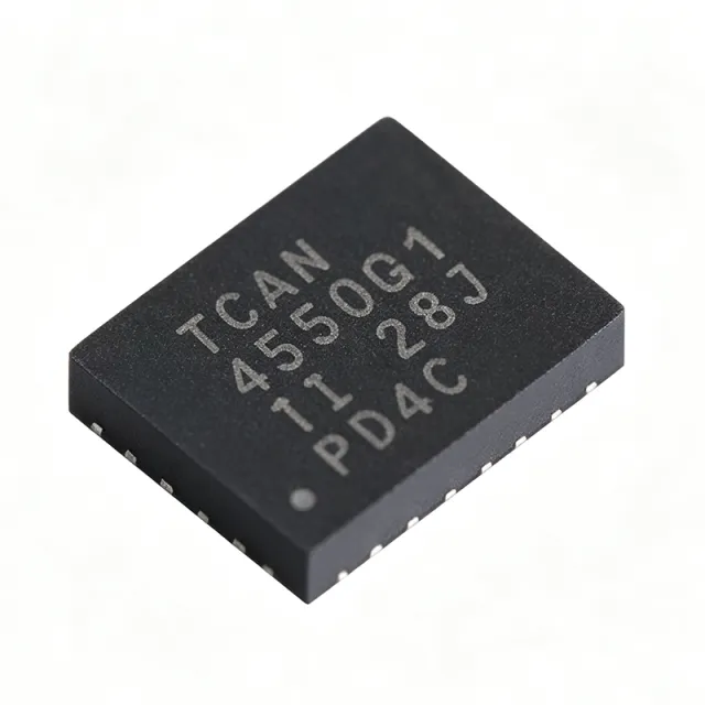
TCAN4550RGYRQ1 - CAN FD SBC with Transceiver 8Mbps VQFN-20 | TI
The Texas Instruments TCAN4550RGYRQ1 is an automotive system basis chip (SBC) that integrates a CAN FD controller and a CAN FD transceiver supporting data rates up to 8 Mbps in a 20-pin VQFN (RGY) package measuring 3.5 x 4.5 mm. It is AEC-Q100 qualified for operation across the -40C to +125C automotive temperature range and interfaces to the host microcontroller through an SPI bus, enabling a single-chip CAN FD node with minimal external components. A CAN FD (Controller Area Network Flexible Data Rate) system basis chip is an integrated mixed-signal IC that combines the ISO 11898-1 data link layer controller, the ISO 11898-2 physical layer transceiver, and an internal logic LDO into a single package. The CAN FD protocol extends classic CAN by allowing a higher data payload and a flexible bit rate, enabling automotive networks to scale from 1 Mbps to 8 Mbps while preserving the deterministic arbitration of classic CAN. Integrating the controller and the transceiver on one die reduces PCB area, removes the high-speed digital signals between two separate ICs, and improves EMC robustness versus discrete controller-plus-transceiver implementations. Key specifications of the TCAN4550RGYRQ1 include CAN FD data rates up to 8 Mbps, ISO 11898-2:2016 physical layer compliance, an SPI host interface up to 10 MHz, integrated 5V/3.3V selectable LDO for VCC logic supply, low-power standby and sleep modes, and a watchdog timer. The 20-pin VQFN package with exposed thermal pad supports automotive power profiles while staying within a 3.5 x 4.5 mm footprint suitable for space-constrained ECUs. The TCAN4550-Q1 uses a high-speed CAN transceiver with explicit bus-fault protection, thermal shutdown, and wide common-mode range for reliable communication on 12V automotive bus networks. The on-chip LDO generates the logic supply from the 5V CAN rail, removing the need for an external regulator in many applications. SPI registers expose CAN ID filters, bit-timing parameters (sample point and propagation delay), and diagnostic counters, which simplifies firmware bring-up. Typical applications include automotive body control modules, gateways, battery management systems (BMS), powertrain ECUs, ADAS sensor nodes, and industrial CAN FD networks. The 8 Mbps capability is particularly valuable for high-throughput diagnostics and emerging zonal architectures in modern vehicles. Designers should connect the exposed pad to a solid ground plane for thermal dissipation, place 100 nF + 1uF decoupling close to VCC and VIO pins, and follow ISO 11898-2 bus-termination guidance (60 ohm / 120 ohm) on the CANH/CANL differential pair. Verify SPI mode 0 timing against microcontroller datasheet before enabling CAN bus activity. This page synthesizes distributor pricing, drop-in alternatives, and design considerations not consolidated in the manufacturer datasheet.
TCAN843-Q1 - 5Mbps CAN FD Transceiver Sleep | TI
The Texas Instruments TCAN843-Q1 is an automotive-grade, high-speed Controller Area Network (CAN) transceiver meeting the physical layer requirements of the ISO 11898-2:2024 high-speed CAN specification. It supports both classical CAN and CAN FD data rates up to 5 Mbps and is offered in 14-pin leaded (SOT and SOIC) and leadless (VSON) packages with wettable flanks for improved automated optical inspection (AOI). A CAN transceiver is the physical-layer interface between a CAN controller in a microcontroller and the differential twisted-pair bus. It converts logic-level TXD/RXD signals into differential CANH/CANL signals, providing the drive strength, fault tolerance, and noise immunity required in harsh automotive and industrial environments. Key features include 5 Mbps CAN FD support, four operating modes (normal, silent, standby, and low-power sleep), and a VIN pin tied to the microcontroller I/O supply that supports a 3.3V to 5.5V logic range. The INH output pin enables system-level battery-current reduction by selectively gating power supplies, allowing a low-current sleep state while the transceiver monitors the bus for wake-up frames. Protection features include thermal shutdown (TSD), TXD-dominant time-out (TXD DTO), load-dump support on VSUP, undervoltage protection, and CAN bus fault tolerance in 12V and 24V systems. The robust bus interface with high ESD tolerance ensures reliable operation in body electronics, gateways, and battery management systems. Typical applications include body control modules, gateway modules, battery management systems, and industrial transportation networks where always-on nodes must minimize quiescent battery drain while maintaining network responsiveness. When designing with the TCAN843-Q1, use proper 120-ohm bus termination, place the transceiver close to the connector to minimize stub length, and connect VIN to the microcontroller I/O supply to set the digital interface logic level.

TCKE501UA - 1.7V-5.5V 1A eFuse IC 75mΩ SOT-353F | Toshiba
The Toshiba TCKE501UA is a 1.0 A single-channel eFuse IC (hot-swap protection IC) operating from a 1.7 V to 5.5 V input range, with a typical on-resistance of 75 mΩ, housed in the compact 5-pin SOT-353F (UFV) surface-mount package. An eFuse IC, or electronic fuse, is an integrated circuit protection device that sits in series with a power rail and replaces a traditional resettable fuse or discrete MOSFET-based hot-swap circuit. Within the power management IC hierarchy, eFuse ICs sit alongside hot-swap controllers and load switches, providing overcurrent, short-circuit, and overtemperature protection in one small footprint, with fast response times that conventional fuses cannot match. Key features of the TCKE501UA include adjustable overcurrent protection set by a single external resistor, integrated short-circuit protection, and thermal shutdown (overheat protection). Its low 75 mΩ typical on-resistance minimizes voltage drop and power loss in the protected rail, while the wide 1.7 V to 5.5 V operating range makes it one of the first Toshiba eFuse ICs to support 1.8 V low-voltage rails alongside 3.3 V and 5 V systems. The 1.0 A maximum output current suits protection of low-power digital loads. The TCKE5 series integrates the power MOSFET, current-sense circuitry, and protection logic on a single die, reducing bill-of-material count versus discrete solutions. During a fault, the internal control loop limits or interrupts current within microseconds, and the device automatically recovers once the fault and thermal condition clear, acting as a reusable fuse. The small SOT-353F package conserves board area in space-constrained designs. Typical applications include consumer equipment, IoT devices, and general-purpose power supplies - for example, protecting 1.8 V DDR or sensor-rail power lines, 3.3 V microcontroller supplies, and 5 V USB-derived rails in battery-powered and mains-powered products. When designing with the TCKE501UA, size the external ILIM resistor for the desired overcurrent threshold per the manufacturer datasheet, and account for the 75 mΩ on-resistance drop at full load (about 75 mV at 1 A). This page synthesizes distributor availability, drop-in same-family alternatives, and practical design notes not found in the manufacturer datasheet.
TCKE501UL - 1A eFuse IC, 75mΩ, 1.7-5.5V | Toshiba | SOT-353F
The Toshiba TCKE501UL is a 1 A single-input single-output eFuse IC (electronic fuse) for advanced power-line protection, operating from 1.7 V to 5.5 V input with a typical on-resistance of 75 mΩ, housed in the small SOT-353F (UFV) package. An eFuse IC is a type of electronic circuit protector that replaces a traditional resettable fuse (PPTC) or discrete fuse circuit in a power distribution path. Within the power management IC hierarchy, the eFuse sits alongside hot-swap controllers and load switches as a protection device: it monitors input current and voltage, and disconnects the load when an overcurrent, short-circuit, or overtemperature event is detected, protecting both upstream supply and downstream load. Key features of the TCKE5 Series include adjustable overcurrent protection set by an external resistor on the ILIM pin, built-in short-circuit protection with fast response, and overheat (thermal) protection. The 75 mΩ typical on-resistance minimizes voltage drop and power loss at the full 1 A output current. The 1.7 V minimum operating voltage is a differentiating specification, supporting modern 1.8 V power rails used in low-voltage consumer, IoT, and portable designs. Architecturally, the TCKE5 Series integrates a sensing FET, control logic, and protection circuits in a single low-cost package. The UL suffix denotes the latch-type fault response variant of the family (the UA variant provides the auto-retry behavior), letting designers choose recovery behavior per system policy. Thermal protection shuts the internal FET off if die temperature exceeds the protection threshold, and the device acts as a reusable fuse across repeated fault events. Typical applications include USB device power-line protection, HDMI equipment, laptop PCs, gaming consoles, IoT equipment, and general-purpose power supplies. Wherever a 1.8 V to 5 V rail feeds an external connector or unprotected load, the TCKE501UL provides compact turnkey fault isolation. Design consideration: set the overcurrent threshold with the ILIM resistor per the datasheet equation, verify PCB copper area for thermal dissipation at sustained load, and follow the precautions detailed in the manufacturer datasheet for latch-type behavior. This page adds distributor-style comparison data, drop-in same-family alternatives, and practical design notes not found in the Toshiba datasheet.
TCKE502UA - 1.7-5.5V 1A eFuse IC 75mΩ SOT-353F | Toshiba
The Toshiba TCKE502UA is a single-input, single-output eFuse IC (electronic fuse) supporting line-voltage inputs from 1.7 V to 5.5 V with up to 1.0 A output current, an ultra-low typical on-resistance of 75 mΩ, housed in a compact 5-pin SOT-353F (UFV) surface-mount package. An eFuse IC is a solid-state circuit-protection device that functions as a resettable, reusable fuse within the power-management IC hierarchy. Unlike a one-time fusible link or a PTC resettable fuse, an eFuse integrates a MOSFET pass element, current-sense circuitry, and control logic in one IC, allowing designers to set precise overcurrent thresholds, block short-circuit faults within microseconds, and shut down on overtemperature. eFuses sit between the power source and the load, guarding hot-swap rails, USB ports, and low-voltage digital supplies. Key features of the TCKE502UA include adjustable overcurrent protection set by a single external resistor, fast short-circuit protection, thermal shutdown with automatic recovery behavior, and the low 75 mΩ on-resistance that minimizes voltage drop and conduction power loss at the full 1.0 A load. Its 1.7 V minimum input uniquely supports 1.8 V power rails used in modern low-voltage IoT devices, a capability highlighted in Toshiba's October 2026 launch announcement of the TCKE5 series. The TCKE5 series uses a simple single-channel architecture: the internal N-channel MOSFET pass device is controlled by protection logic, so external circuitry is limited to an ILIM-setting resistor and standard input/output decoupling capacitors. This reduces bill-of-material complexity compared with discrete hot-swap controller plus MOSFET solutions. The SOT-353F package saves board area versus larger eFuse options in WDFN or SOIC packages. Typical applications include consumer equipment, IoT devices, general-purpose power supplies, 1.8 V and 3.3 V rail protection on microcontroller boards, and hot-swap input protection for battery-powered portable products. Design consideration: size the external current-limit resistor so the trip threshold sits above the load's worst-case inrush and transient current, and verify thermal margins since 75 mΩ at 1.0 A dissipates an estimated 75 mW. This page adds information gain by synthesizing distributor availability data (Farnell/element14), the Toshiba TCKE5 datasheet, series-family drop-in alternatives, and practical design notes in one place.
TCKE502UL - 1A eFuse IC, 75mΩ, SOT-353F | Toshiba
The Toshiba TCKE502UL is a single-input, single-output eFuse IC (electronic fuse) supporting line-voltage inputs from 1.7V to 5.5V with an output current of up to 1.0A and a low on-resistance of 75 mΩ (typical), housed in the small SOT-353F (UFV) package. An eFuse IC is a reusable, resettable electronic circuit-protection device that replaces disposable fuses and discrete protection circuits in a power path. Positioned within the power management IC hierarchy (eFuse IC -> hot-swap protection IC -> voltage regulator family -> power management IC), it combines a power MOSFET switch with protection logic: when an overcurrent, short-circuit, or over-temperature event occurs, the device rapidly turns off the power path and can later be reset, protecting downstream loads such as SoCs, sensors, and wireless modules. Key features of the TCKE502UL include adjustable overcurrent protection set by a single external resistor, fast short-circuit protection, thermal shutdown, and a low 75 mΩ on-resistance that minimizes voltage drop and power loss at the full 1A load. The 1.7V minimum input makes it suitable for modern 1.8V rails, and the SOT-353F package occupies minimal board area for space-constrained designs. The TCKE5 Series is Toshiba's low-voltage eFuse family; the lineup comprises four products, TCKE501UA, TCKE501UL, TCKE502UA, and TCKE502UL, all housed in the SOT-353F (UFV) package, with suffix distinctions covering latch-type versus auto-retry behavior between the 501 and 502 variants. The low-voltage capability addresses the growing use of 1.8V power lines driven by miniaturization and lower power consumption in IoT and consumer equipment. Typical applications include IoT equipment power rails, consumer equipment, general-purpose power supplies, USB accessory ports, battery-powered portable devices, and post-regulator protection after DC-DC converters on 1.8V to 5V rails. When designing with this device, size the external ILIM resistor for the desired overcurrent threshold with margin above the maximum load current, and verify the thermal rise across the 75 mΩ on-resistance at continuous full load. This page synthesizes distributor availability data, same-series drop-in options, and practical design notes not found in the manufacturer datasheet. Pricing references are as of 2026-10-19.

TCKE712BNL - 13.2V 3.65A eFuse IC, 53mΩ | Toshiba
The Toshiba TCKE712BNL is a 13.2 V input eFuse IC (electronic fuse) with an adjustable overcurrent limit, 53 mΩ typical on-resistance, and a 3.65 A maximum continuous output current, housed in a 10-pin WSON (3x3 mm) package. It functions as a resettable, single-input single-output circuit-protection IC for 4.4 V to 13.2 V power rails. An eFuse IC is a solid-state electronic fuse integrated into a power-management IC: it sits in series with a supply rail and disconnects the load when current, voltage, or temperature conditions exceed safe limits. Unlike a one-time熔 fuse, an eFuse can be re-enabled after a fault, and unlike a hot-swap controller alone it integrates the power MOSFET, sense element, and control logic in one package. eFuses sit in the broader hierarchy of power management ICs, alongside LDO regulators, DC-DC converters, and supervisors, and are a standard building block in server, storage, IoT, and general-purpose power supplies. Key features include an adjustable overcurrent limit set by a single external resistor, short-circuit protection with fast response, programmable inrush (slew rate) control via an external capacitor, and adjustable overvoltage protection with undervoltage lockout. The 53 mΩ on-resistance minimizes series voltage drop and power loss - at a 3 A load the drop is only about 159 mV and dissipation about 0.48 W (estimated: I²R = 3² × 0.053). Technically, the TCKE712BNL is a CMOS silicon-monolithic linear power IC. The integrated back power MOSFET and sense circuitry enable precise current limiting, while the slew-rate control pin allows designers to soft-start capacitive loads and suppress inrush spikes during hot-plug events. Fault behavior (latch-off versus auto-retry) is handled by the BL series variant family, letting designers match protection policy to system requirements. Typical applications include server backplane 12 V rail protection, SSD and hard-disk storage power inputs, IoT equipment and consumer electronics DC inputs, and general-purpose 5 V/12 V power-supply outputs where a resettable fuse with inrush control is required. Design consideration: set the overcurrent limit resistor so the trip point sits above the worst-case load transient but well below the wiring and connector ratings, and choose the slew-rate capacitor for the load capacitance to keep inrush below the OCP threshold during startup. This page synthesizes distributor pricing, same-family drop-in alternatives, comparison tables, and practical eFuse design notes not found in the manufacturer datasheet alone.
TCKE712BNL,RF - 13.2V 5A eFuse IC WSON10 | Toshiba
The Toshiba TCKE712BNL,RF is a 13.2 V input single-input, single-output eFuse IC with an adjustable overcurrent limit, 56 mOhm on-resistance, and 5 A peak current capability, housed in a 10-pin WSON (WSON10) leadless package. It functions as a resettable, reusable electronic fuse for advanced circuit protection on 5 V and 12 V power rails. An eFuse IC (electronic fuse) is a type of power-management protection IC that sits in series with a supply rail and disconnects the load when fault conditions such as overcurrent, short circuit, overvoltage, or undervoltage occur. Unlike a one-time fuse, an eFuse can automatically or manually recover after a fault, making it a building block of modern power management IC architectures in servers, storage systems, IoT devices, and general-purpose power supplies. Key features of the TCKE712BNL include an adjustable overcurrent limit set by a single external resistor, adjustable overvoltage protection (OVP) and undervoltage lockout (UVLO), short-circuit fast-trip protection, and an adjustable output slew rate controlled by an external capacitor, which limits inrush current during hot-plug and capacitive load start-up. The device also integrates reverse current blocking (RCB) and a fault flag output for system-level fault reporting. Technically, the part operates from a 4.4 V to 13.2 V input range, covering 5 V, 9 V, and 12 V rails from a single orderable device. The internal low-RDS(on) power MOSFET (about 53-56 mOhm) minimizes voltage drop and conduction loss, while a controlled gate-slew architecture keeps source-to-load turn-on monotonic. Thermal shutdown protects the die under sustained fault conditions, and the flag pin signals fault state to the host controller. Typical applications include server backplane hot-swap protection, SSD and HDD storage rail protection, IoT node power-path protection, USB and 12 V accessory ports, and general-purpose industrial power supplies where a reusable fuse with adjustable trip points is preferred over discrete fuse plus supervisor circuits. A key design consideration: size the ILIM resistor so the minimum guaranteed current limit exceeds the worst-case load transient, and set the slew-rate capacitor to balance inrush limiting against acceptable startup time; excessive capacitance on the output increases startup duration. This page synthesizes distributor pricing, same-family drop-in alternatives, practical design notes, and comparison data not consolidated in the manufacturer datasheet, as of 2026-10-19.